

Page 1
LCD MONITOR
SERVICE MANUAL
CAUTION
BEFORE SERVICING THE CHASSIS,
READ THE SAFETY PRECAUTIONS IN THIS MANUAL.
CHASSIS : MF-02HA
MODEL : MW-30LZ10
website:http://biz.LGservice.com
e-mail:http://www.LGEservice.com/techsup.html
Aug., 2002
Printed in KoreaP/NO : 3828VD0120B
Page 2

- 2 -
CONTENTS
Contents .................................................................................................. 2
Safety Precautions ..................................................................................3
Adjustment Instruction ............................................................................4
Troubleshooting .......................................................................................6
Printed Circuit Board ...............................................................................7
Block Diagram.........................................................................................11
Exploded View ...................................................................................... 16
Exploded View Parts List.......................................................................17
Replacement Parts List ........................................................................ 18
SVC. Sheet .................................................................................................
Page 3
- 3 -
SAFETY PRECAUTIONS
Many electrical and mechanical parts in this chassis have special safety-related characteristics. These parts are identified by in
the Schematic Diagram and Replacement Parts List.
It is essential that these special safety parts should be replaced with the same components as recommended in this manual to
prevent X-RADIATION, Shock, Fire, or other Hazards.
Do not modify the original design without permission of manufacturer.
General Guidance
An lsolation Transformer should always be used during
the servicing of a receiver whose chassis is not isolated from
the AC power line. Use a transformer of adequate power rating
as this protects the technician from accidents resulting in
personal injury from electrical shocks.
It will also protect the receiver and it's components from being
damaged by accidental shorts of the circuitary that may be
inadvertently introduced during the service operation.
If any fuse (or Fusible Resistor) in this TV receiver is blown,
replace it with the specified.
When replacing a high wattage resistor (Oxide Metal Film
Resistor, over 1W), keep the resistor 10mm away from PCB.
Keep wires away from high voltage or high temperature parts.
Due to high vacuum and large surface area of picture tube,
extreme care should be used in handling the Picture Tube.
Do not lift the Picture tube by it's Neck.
Before returning the receiver to the customer,
always perform an AC leakage current check on the exposed
metallic parts of the cabinet, such as antennas, terminals, etc.,
to be sure the set is safe to operate without damage of
electrical shock.
Leakage Current Cold Check(Antenna Cold Check)
With the instrument AC plug removed from AC source,
connect an electrical jumper across the two AC plug prongs.
Place the AC switch in the on positioin, connect one lead of
ohm-meter to the AC plug prongs tied together and touch other
ohm-meter lead in turn to each exposed metallic parts such as
antenna terminals, phone jacks, etc.
If the exposed metallic part has a return path to the chassis, the
measured resistance should be between 1MΩ and 5.2MΩ.
When the exposed metal has no return path to the chassis the
reading must be infinite.
An other abnormality exists that must be corrected before the
receiver is returned to the customer.
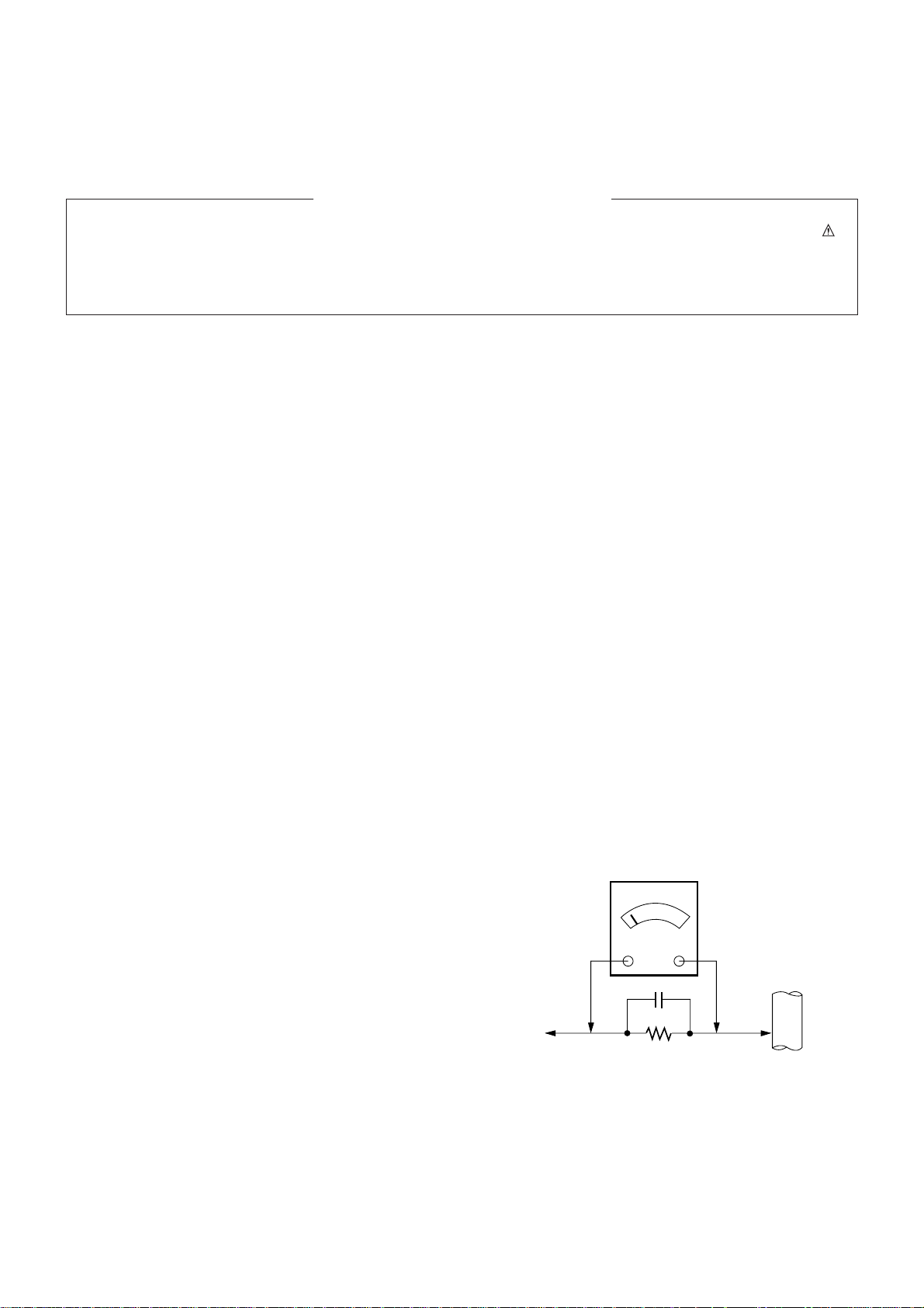
Leakage Current Hot Check (See below Figure)
Plug the AC cord directly into the AC outlet.
Do not use a line Isolation Transformer during this check.
Connect 1.5K/10watt resistor in parallel with a 0.15uF capacitor
between a known good earth ground (Water Pipe, Conduit, etc.)
and the exposed metallic parts.
Measure the AC voltage across the resistor using AC
voltmeter with 1000 ohms/volt or more sensitivity.
Reverse plug the AC cord into the AC outlet and repeat AC
voltage measurements for each esposed metallic part. Any
voltage measured must not exceed 0.75 volt RMS which is
corresponds to 0.5mA.
In case any measurement is out of the limits sepcified, there is
possibility of shock hazard and the set must be checked and
repaired before it is returned to the customer.
Leakage Current Hot Check circuit
1.5 Kohm/10W
To Instrument's
exposed
METALLIC PARTS
Good Earth Ground
such as WATER PIPE,
CONDUIT etc.
AC Volt-meter
IMPORTANT SAFETY NOTICE
0.15uF
Page 4

- 4 -
1. Application Object
These instructions are applied to all of the MODELS of LCD
MONITOR, MF-02HA.
2. Notes
(1) Because this is not a hot chassis, it is not necessary to use
an isolation transformer. However, the use of isolation
transformer will help protect test instrument.
(2) Adjustment must be done in the correct order. But, it can
be changed in consideration of mass production.
(3) The adjustment must be performed in the circumstance of
25±5°C of temperature and 65±10% of relative humidity if
there is no specific designation.
(4) The input voltage of the receiver must keep 220V, 60Hz in
adjusting.
[ Input voltage is possible from 85V to 260V because the
power voltage applied to this chassis is Wide-Range. But,
adjustment should be operated in 220V/60Hz if there is no
specific designation.
(5) The receiver must be operated for about 15 minutes prior
to the adjustment.
¤ After receiving 100% white pattern(06CH), the receiver
must be operate prior to adjustment.(Or white condition
in HEAT-RUN mode)
¤ŁEnter into HEAT-RUN mode
- Select HEAT RUN OFF by pressing ADJ button on
Remote Control for adjustment.
- Press the VOL + button in HEAT-RUN OFF.
(OSD displays HEAT-RUN WHITE and screen
displays 100% full WHITE PATTERN)
[ Set is activated HEAT-RUN without signal generator
in this mode.
[ Single color pattern of HEAT-RUN mode can be used
to check PANEL.(RED/BLUE/GREEN)
[Caution] If you turn on a still screen more than 20 minutes
(especially, Digital pattern[13 CH], Cross Hatch
Pattern[09CH]), a afterinage may be occur in the black
level part of the screen.
3. Adjustment Items
3-1. Whole Assembly Adjustment
(1) White Balance Adjustment
(2) SUB-BRIGHT Adjustment : Sub-Bright adjustment in LCD
panel is not necessary. Do not adjust sub-bright if there is
no specific designation.
(3) RGB CUT-OFF Adjustment : Under examination about
auto adjustment which correspond to the new Rembrandt1A.
3-2. EDID (The Extended Display
Identification Data) Adjustment
(1) This is the function that is made for the realization of “Plug
and Play” which makes possible to use the user
environment right after reorganization by communicating
with monitor automatically.
(2) EDID DATA for DVI of MF-02HA
EDID table =
00 01 02 03 04 05 06 07 08 09
_________________________________
000 | 00 FF FF FF FF FF FF 00 1E 6D
010 | D7 3A 01 01 01 01 33 0B 01 01
020 | 81 40 26 96 08 B7 FB A1 56 48
030 | 98 24 13 48 4B AF EF 00 81 00
040 | 31 59 45 59 61 59 81 80 71 4F
050 | 01 01 01 01 BC 34 00 98 51 00
060 | 2A 40 10 90 13 00 40 26 00 00
070 | 00 1E 00 00 00 FC 00 4D 57 20
080 | 33 30 4C 5A 31 30 0A 20 20 20
090 | 00 00 00 FD 00 3C 78 1F 5B 10
100 | 00 0A 20 20 20 20 20 20 D5 09
110 | 80 A0 20 E0 2D 10 10 60 A2 00
120 | EE F0 75 00 00 18 00 BD
(3) EDID DATA for RGB of MF-02HA
EDID table =
00 01 02 03 04 05 06 07 08 09
__________________________________
000 | 00 FF FF FF FF FF FF 00 1E 6D
010 | D7 3A 01 01 01 01 33 0B 01 01
020 | 1E 40 26 96 08 B7 FB A1 56 48
030 | 98 24 13 48 4B AF EF 00 81 00
040 | 31 59 45 59 61 59 81 80 71 4F
050 | 01 01 01 01 BC 34 00 98 51 00
060 | 2A 40 10 90 13 00 40 26 00 00
070 | 00 1E 00 00 00 FC 00 4D 57 20
080 | 33 30 4C 5A 31 30 0A 20 20 20
090 | 00 00 00 FD 00 3C 78 1F 5B 10
100 | 00 0A 20 20 20 20 20 20 D5 09
110 | 80 A0 20 E0 2D 10 10 60 A2 00
120 | EE F0 75 00 00 18 00 BD
(4) Refer to Service Manual related to EDID communication.
4. Whole Assembly Adjustment
<Caution> Each PCB Assy must be checked by Check JIG Set
before assemling.(Be careful about power PCB ASSY
which can give a fatal damage to the LCD Module)
4-1. White Balance Adjustment
(1) Required Equipment
Color analyzer(CA-100 or same production)
ADJUSTMENT INSTRUCTION
Page 5

- 5 -
(2) Connection Diagram of Equipment for
Measuring (Automatic Adjustment)
Connect RS-232C to Adjustment Equipment and SET.
Automatization operating room has in charge of managing and
repairing about adjusting equipment.
Only adjust HIGH LIGHT and RGB input adjusts R-GAIN/GGAIN/B-GAIN automatically.
Automatic adjustment equipment decides the values of RGAIN/G-GAIN/B-GAIN by correcting color coordinates/white
balance and transmits them into SET and finally the SET
saves data values.
(3) White Balance Adjustment(Manual Adjustment)
¯ Operate Zero Calibration of CA-100 and Sensor must be
stick completely to the surface of LCD module
¯ Devide Manual adjustment into AV/PC and operate
adjustment by the following sequence.
¯ Manual adjustment is a temporary method when automatic
adjustment is not correspondent.
1. AV W/B adjustment
1) Select WHITE PATTERN of HEAT RUN mode by
pressing ADJ button on Remote Control for adjustment
then operate HEAT RUN more than 15 minute
2) Supply pattern signal for WB adjustment in pattern
generator. (AV INPUT)
3) Low Light has no special adjustment.
4) To adjust High Light, stick sensor to 2th pattern(White),
select and adjust the AV GAIN by pressing INSTSRT
button on Remote Control for adjustment.
After select the R GAIN and G GAIN, enter Adjustment
Mode by pressing ENTER button and press the VOL +/Key and adjust it until color coordination becomes (B
GAIN is fixed)
color coordination : X=0.283±0.003, Y=0.296±0.003
color temperature : 9,350°K ± 500°K
5) Exit adjustment mode using Enter button.
2. PC W/B Adjustment
1) Select WHITE PATTERN of HEAT RUN mode by
pressing ADJ button on Remote Control for adjustment
then operate HEAT RUN more than 15 minute.
2) Supply pattern signal for WB adjustment in pattern
generator.(RGB1 INPUT)
3) Low Light has no special adjustment.
4) To adjust High Light, stick sensor to 2th pattern(White),
select and adjust the PC GAIN by pressing INSTSRT
button on Remote Control for adjustment.
After select the R GAIN and G GAIN, enter Adjustment
Mode by pressing ENTER button and press the VOL +/-
Key and adjust it until color coordination becomes (B
GAIN is fixed)
color coordination : X=0.283±0.003, Y=0.296±0.003
color temperature : 9,350°K ± 500°K
(R Gain is used to adjust X-coordinates while adjusting
and X-coordinates could be shortened when R Gain is
increased.
G Gain is used to adjust Y-coordinates while adjusting
andY-coordinates could be shortened when G Gain is
increased.)
5) Exit adjustment mode using Enter button.
3. Component (480p~1080i) Offset Adjustment
¯ Use this adjustment when the Grayscale out of Ch13.
Pattern has red or blue while producing set.
¯ This adjustment is used to remove the declination of
YPbPr Offset in AD9888.
1) Operate the adjustment after PC/AV White Balance
adjustment progress.
2) Select Ch.14 after connect DTV STB to Component
(480p~1080i) terminal and AV terminal.
3) When you press ADJ button twice on the R/C for
adjustment, the SET goes to DWI condition and Main
Window(right side)/Sub Window(left side) are set to AV
mode.
4) In this condition, adjust R with ‘DTV R OFFSET’ and B
with ‘DTV B OFFSET’ based on ‘foundation color(Gray)’
of Ch.14.
5) Exit adjustment mode using Enter button.
Window
MASTER or
QUANTUM DATA
COLOR
ANALYZER
TYPE;CA-100
RGB Signal Input
LCD MONITOR
High Light
450±70cd/m
2
(Fig. 1) Connection Diagram of Automatic Adjustment
Page 6

- 6 -
Symptom Cause Check Point
1) Check BD801, Q801, Q802, Q804
2) Check BD801, L801, L802, TH800, TH801
1) Check the second side parts and Pattern short
2) Check reverse input of PH801, D916, CR802
3) Check R941~R944 when the Pin Bias power no7. of
U902 is abnormal. (normal: 15V~25V)
- Replace U902(FAN7554) parts
- Check the error of Q804
4) Replace T803
1) Check the peripheral parts of 18V and Pattern short.
2) Check reverse input of D916(SB560)
3) No Input of L812 when both terminal voltage of C830
are low. (normal voltage: +24V)
- Replace U802(PQ1CG203) parts when there is no
error.
1) Check the peripheral parts of 5VS and Pattern short.
2) Check reverse input of D802, CR801
3) Check R937~R939 when the Pin Bias power no7. of
U903 is abnormal. (normal: 15V~25V)
- Replace U903(FAN7554) parts
- Check the error of Q802
4) Replace T802
1) Replace U901(MC33368D) when there is no error in
the peripheral parts.
- Check the error of Q801
2) Replace T801
1) Fuse open
2) Error of rectying circuit/EMI Filter
1) Short of output terminal
2) Input error of parts
3) Error of U902 and peripheral circuits.
4) Error of T803
1) Short of output terminal
2) Input error of parts
3) Error of U802 and peripheral circuits.
1) Short of output terminal
2) Input error of parts
3) Error of U903 and peripheral circuits.
4) Error of T802
1) Drop of output power due to the error
of PFC circuit.
2) Error of T801
1. No power from all outputs
2. No power from +24V/+12V
/+18V
3. No power from +18V
4. No power from +5VS
5. No power from +24V/+12V
/+18V in 110VAC Input
TROUBLESHOOTING
Page 7
- 7 -
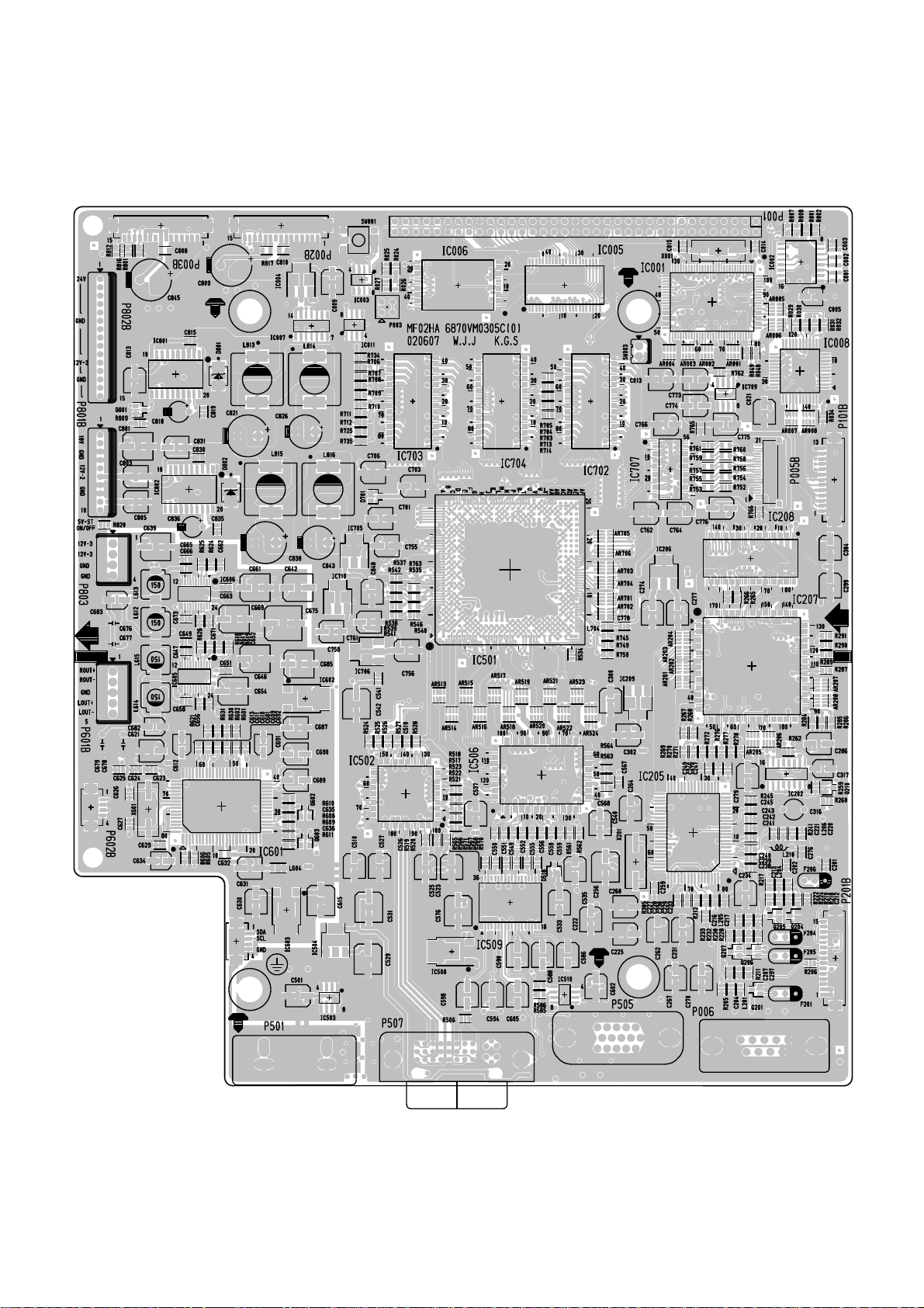
PRINTED CIRCUIT BOARD
MAIN(TOP)
Page 8

- 8 -
MAIN(BOTTOM)
Page 9

- 9 -
SIDE A/V(TOP)
SIDE A/V(BOTTOM)
Page 10

- 10 -
CONTROL(TOP)
POWER(TOP) POWER(BOTTOM)
CONTROL(BOTTOM)
Page 11

- 11 -
BLOCK DIAGRAM
1. VSC Board
Page 12

- 12 -
2. System Block Diagram & Function
2-1. Input Source Ranges
(1) Input Paths
: CVBS, S-Video, Component (480i, 480p, 720p, 1080i), RGB 1, RGB 2, RS-232C
(2) Video System Recognition (Multi-system ; Refer to Product Specification)
: NTSC M, NTSC 4.43, PAL, PAL M, PAL N, PAL 4.43, SECAM
(3) RGB 1 Mode Compatibility
: Up to SXGA 75Hz (See Compatibility Table in Product Specification in detail.)
(4) RGB 2 Mode Compatibility
: Up to SXGA 60Hz (See Compatibility Table in Product Specification in detail.)
2-2. Video Controls
(1) RGB Video Controls
: Contrast, Brightness, Color Red, Color Green, Color Blue, User Setting Reset
: Clock, Phase, Auto Tracking (Automatic Clock & Phase Optimization)
(2) AV Video Controls (AV1, AV2, S-Video, Component 1, Component 2)
: Contrast, Brightness, Color Level(Saturation), Tint(Hue), Sharpness, User Setting Reset
¡ See the OSD Spec. for more detail information of video controls.
2-3. Audio Controls
(1) Volume, Treble, Bass, Balance Control
(2) Sound Mute
Page 13

- 13 -
3. Power
Page 14

- 14 -
3-1. Explanation of Circuit Movement
If the AC Input voltage(1) is confirmed to power device, this Input voltage is adjusted as DC wave form through EMI
FILTER(2) and the first adjusting part(3). This adjusted wave form is input to PFC(4, Power Factor Correction) and makes
the PFC circuit works and the output voltage(+390Vdc) by PFC circuit becomes a Main Input voltage of MAIN(5),
STANBY(10) Switching part.
Input voltage is input to Switching part(5, 10) and make this High voltage DC voltage(390Vdc) to be a High Voltage
spherical wave with high frequency through the Switching by the elements such as FET, PWM IC.
To keep the secondary adjusted voltage to be regular and safe in changing Input voltage and Output load, the output voltage
is watched and feedback to switching part(5, 10) through the control circuit(9).
BLOCK 2 works as Forward converter method by receiving Input of BLOCK 1 and supplies MAIN DC(+24V, +12V) voltage
and the Step Down circuit(8) supplies +18V.
Also, BLOCK 3 works as Flyback converter method by receiving Input of BLOCK 1 and supplies +5V for Stanby.
Protection circuit is built in switching part(5, 10) to protect over electric-current, short, over voltage of the secondary output.
This circuit protects the output and stick the Terminal Switch(15) to radiator while PFC and protect a fire or other accident by
turning the AC voltage off while overheating.
To minimize power consumption, if the OFF signal is transmitted to PFC part(4), Main part(5) through the control circuit
connected from Main board to Power board, only the +5V circuit for Standby works and others are OFF.
Page 15

MEMO
- 15 -
Page 16

- 16 -
EXPLODED VIEW
112
300
400
520
501
530
580
531
420
410
550
551
540
570
943
Page 17

- 17 -
EXPLODED VIEW PARTS LIST
112 6305V00001A LCD ASSEMBLY,30” LCD PANEL LC30W01-A3 AND I
300 3091V00A73E CABINET ASSEMBLY
400 3809V00A33B BACK COVER ASSEMBLY
3809V00A33D BACK COVER ASSEMBLY
410 3501V00083A BOARD ASSEMBLY,BASE MW-30LZ10
420 3508V00306A DECO,REAR COVER
501 4980V00505B SUPPORTER ASSY,MODULE
520 6871VMN648A PCB ASSEMBLY,MAIN MF-02HA MW-30LZ10 MAIN BO
6871VMN637A PCB ASSEMBLY,MAIN MF-02HA MW-30LZ10 MAIN BO
530 6871VSN182B PCB ASSEMBLY,SUB A/V MF-02HA MW-30LZ10 AV BOARD
531 4930V00226E HOLDER,AV
540 3141VPN048A CHASSIS ASSEMBLY,SMPS MF-02HA LCD30 SWITCH
550 6871VSN181A PCB ASSEMBLY,SUB SPK MF-02HA MW-30LZ10 SPK BOAR
551 4930V00224C HOLDER,SPK JACK
560 6633VA0004A INVERTER ASSEMBLY,24VOLT 1100VOLT K.S. KLS300W1
570 6871VSN180A PCB ASSEMBLY,SUB CONT MF-02HA MW-30LZ10 CONTROL
580 3501V00091A BOARD ASSEMBLY,SMPS PFC MW-30LZ10 MF-02HA LCD
943 1FBF0403122 SCREW,D4.0 L16.0
No.
PART NO.
DESCRIPTION
Page 18

REPLACEMENT PARTS LIST
LOCA. NO PART NO DESCRIPTION
IC802
IC709
Q01
Q02
Q201
Q203
Q204
Q205
Q206
Q207
Q208
Q209
Q210
Q211
Q212
Q213
Q214
Q301
Q302
Q303
Q304
Q602
Q603
Q604
Q606
Q701
Q801
D001
D003
D004
D005
D006
D201
D202
D203
D204
D205
D501
D502
D503
D504
D505
D506
D507
D508
0IMCRSG003A
0TF492509AA
0TR387500AA
0TR387500AA
0TR387500AA
0TR387500AA
0TR387500AA
0TR387500AA
0TR387500AA
0TR387500AA
0TR387500AA
0TR387500AA
0TR102009AG
0TR387500AA
0TR387500AA
0TR150400BA
0TR387500AA
0TR150400BA
0TR387500AA
0TR150400BA
0TR387500AA
0TR150400BA
0TR150400BA
0TR150400BA
0TR387500AA
0TR102009AG
0TR102009AG
0DD226239AA
0DD226239AA
0DD226239AA
0DD226239AA
0DD226239AA
0DD226239AA
0DD226239AA
0DD226239AA
0DD226239AA
0DD226239AA
0DD226239AA
0DD226239AA
0DD226239AA
0DD226239AA
0DD226239AA
0DD184009AA
0DD226239AA
0DD226239AA
L4973D5.1 SGS-THOMSON 20P SOP
FET,SI4925DY TP TEMIC 30V 6.1A SO
CHIP 2SC3875S(ALY) KEC
CHIP 2SC3875S(ALY) KEC
CHIP 2SC3875S(ALY) KEC
CHIP 2SC3875S(ALY) KEC
CHIP 2SC3875S(ALY) KEC
CHIP 2SC3875S(ALY) KEC
CHIP 2SC3875S(ALY) KEC
CHIP 2SC3875S(ALY) KEC
CHIP 2SC3875S(ALY) KEC
CHIP 2SC3875S(ALY) KEC
CHIP KRC102S SOT-23 TP KEC
CHIP 2SC3875S(ALY) KEC
CHIP 2SC3875S(ALY) KEC
CHIP 2SA1504S(ASY) KEC
CHIP 2SC3875S(ALY) KEC
CHIP 2SA1504S(ASY) KEC
CHIP 2SC3875S(ALY) KEC
CHIP 2SA1504S(ASY) KEC
CHIP 2SC3875S(ALY) KEC
CHIP 2SA1504S(ASY) KEC
CHIP 2SA1504S(ASY) KEC
CHIP 2SA1504S(ASY) KEC
CHIP 2SC3875S(ALY) KEC
CHIP KRC102S SOT-23 TP KEC
CHIP KRC102S SOT-23 TP KEC
CHIP KDS226 SOT-23
CHIP KDS226 SOT-23
CHIP KDS226 SOT-23
CHIP KDS226 SOT-23
CHIP KDS226 SOT-23
CHIP KDS226 SOT-23
CHIP KDS226 SOT-23
CHIP KDS226 SOT-23
CHIP KDS226 SOT-23
CHIP KDS226 SOT-23
CHIP KDS226 SOT-23
CHIP KDS226 SOT-23
CHIP KDS226 SOT-23
CHIP KDS226 SOT-23
CHIP KDS226 SOT-23
KDS184S CHIP 85V 300MA KEC TP
CHIP KDS226 SOT-23
CHIP KDS226 SOT-23
LOCA. NO PART NO DESCRIPTION
IC001
IC002
IC003
IC004
IC005
IC006
IC007
IC008
IC009
IC011
IC201
IC202
IC203
IC204
IC205
IC206
IC207
IC208
IC209
IC501
IC502
IC503
IC504
IC505
IC506
IC508
IC509
IC510
IC511
IC601
IC602
IC603
IC604
IC605
IC606
IC701
IC702
IC703
IC704
IC705
IC706
IC707
IC708
IC710
IC801
0IMCRRS001A
0IDS232000A
0IDS170800A
0ISJ111733A
0IMMRSS064A
0IMMRMR006A
0IPH748600D
0IOK825522A
0IKE704200J
0IAL241610A
0IMCRFA008A
0IFA741230A
0IMCRFA008A
0ISJ111733A
0IIT323000E
0IPRPML001A
0IMCRG2001A
0ISS464323A
0ISJ111733A
0IMCROT001A
0IMCRS5002A
0IAL242110A
0ISJ111733A
0ISJ111733A
0IMCRAD003A
0IMCRFA008A
0IMCRMI006A
0IAL242110A
0IMCRTI001A
0IMCRMN011D
0IMCRFA009A
0IMCRFA008A
0IKE704200J
0IMCRTI015A
0IMCRTI015A
0ISJ111733A
0ISS464323A
0ISS464323A
0ISS464323A
0IMCRSJ001A
0ISJ111733A
0IMCRTH001A
0ISJ111733A
0ISJ111733A
0IMCRSG003A
R8820LV RDC SEMICONDUCTOR LTD
DS232AS 16P,SOP TP RS-232 DRIV
DS1708S 8P SOIC ST MICROMONITO
EZ1117CST-3.3 3P,SOT-223 TP 3.
K6R4016V1C-TC10 SAMSUNG ELECTR
MX29LV160TTC-70 MACRONIX 48P T
74HC86 SOIC-14 TP QUAD 2-INPUT
MSM82C55A-2GS-2K 44P QFP ST CM
KIA7042AF SOT-89 TP 4.2V VOLTA
AT24C16N-10SI 8P SOIC ST EEPRO
KA78M05RTM, FAIRCHILD 2P D-PAK
DM74LS123MX 16SOP TP DUAL RETR
KA78M05RTM, FAIRCHILD 2P D-PAK
EZ1117CST-3.3 3P,SOT-223 TP 3.
VPC3230D C5 80P QFP
MIC39100 MICREL 3P SOT223 R/TP
FLI2200 SAGE 176P,QFP TRAY VID
K4S643232E(C)-TC/L60(70) (KM43
EZ1117CST-3.3 3P,SOT-223 TP 3.
REMBRANT-1A OPLUS TECHNOLOGIES
SIL161BCT RX SILICON IMAGE 100
AT24C21-10SI-2.5 8P,SOP TP 1K
EZ1117CST-3.3 3P,SOT-223 TP 3.
EZ1117CST-3.3 3P,SOT-223 TP 3.
AD9888KS-140 ANALOG DEVICE 128
KA78M05RTM, FAIRCHILD 2P D-PAK
M52758FP MITSUBISHI 36PIN, R/T
AT24C21-10SI-2.5 8P,SOP TP 1K
SN74HCT157D TEXAS INSTRUMENT 1
MSP3410G QA B8 V3 MICRONAS 80P
KA78M08RTM, FAIRCHILD 2P D-PAK
KA78M05RTM, FAIRCHILD 2P D-PAK
KIA7042AF SOT-89 TP 4.2V VOLTA
TPA3000D1 TEXAS INSTRUMENT 24P
TPA3000D1 TEXAS INSTRUMENT 24P
EZ1117CST-3.3 3P,SOT-223 TP 3.
K4S643232E(C)-TC/L60(70) (KM43
K4S643232E(C)-TC/L60(70) (KM43
K4S643232E(C)-TC/L60(70) (KM43
SC1565IST-1.8 SEMTECH 3P SOT22
EZ1117CST-3.3 3P,SOT-223 TP 3.
THC63LVDM83R THINE ELECTRONICS
EZ1117CST-3.3 3P,SOT-223 TP 3.
EZ1117CST-3.3 3P,SOT-223 TP 3.
L4973D5.1 SGS-THOMSON 20P SOP
IC
- 18 -
TRANSISTOR
DIODE
Page 19

- 19 -
LOCA. NO PART NO DESCRIPTION
D509
D510
D511
D512
D513
D514
D515
D516
D517
D518
D519
D520
D521
D522
D523
D524
D525
D526
D601
D602
D603
D604
D701
D702
D801
D802
LD01
ZD501
C005
C009
C013
C016
C021
C222
C225
C231
C234
C238
C239
C240
C241
C256
C260
C262
C264
C267
C270
C274
C277
C279
0DD226239AA
0DD226239AA
0DD226239AA
0DD226239AA
0DD226239AA
0DD226239AA
0DD226239AA
0DD226239AA
0DD226239AA
0DD226239AA
0DD226239AA
0DD226239AA
0DD226239AA
0DD226239AA
0DD226239AA
0DD226239AA
0DD226239AA
0DD226239AA
0DD226239AA
0DD226239AA
0DD181009AB
0DD181009AB
0DD226239AA
0DD226239AA
0DR190309AA
0DR190309AA
0DL200000CA
0DZRM00178A
0CE106SF6DC
0CE476SF6DC
0CE476SF6DC
0CK224DF56A
0CE476SF6DC
0CE476SF6DC
0CE476SF6DC
0CE476SF6DC
0CE476SF6DC
0CK224DF56A
0CK224DF56A
0CK224DF56A
0CK224DF56A
0CE107SF6DC
0CE476SF6DC
0CE476SF6DC
0CE476SF6DC
0CE476SF6DC
0CE476SF6DC
0CE476SF6DC
0CE476SF6DC
0CE476SF6DC
CHIP KDS226 SOT-23
CHIP KDS226 SOT-23
CHIP KDS226 SOT-23
CHIP KDS226 SOT-23
CHIP KDS226 SOT-23
CHIP KDS226 SOT-23
CHIP KDS226 SOT-23
CHIP KDS226 SOT-23
CHIP KDS226 SOT-23
CHIP KDS226 SOT-23
CHIP KDS226 SOT-23
CHIP KDS226 SOT-23
CHIP KDS226 SOT-23
CHIP KDS226 SOT-23
CHIP KDS226 SOT-23
CHIP KDS226 SOT-23
CHIP KDS226 SOT-23
CHIP KDS226 SOT-23
CHIP KDS226 SOT-23
CHIP KDS226 SOT-23
KDS181 TP KEC - 85V - - - 300M
KDS181 TP KEC - 85V - - - 300M
CHIP KDS226 SOT-23
CHIP KDS226 SOT-23
MBRS190T3 TP MOTOROLA - 90V 1A
MBRS190T3 TP MOTOROLA - 90V 1A
LED,SAM5670(DL-2LRG) BK Y-GREEN -
ZENERS,UDZS TE-17 5.1B
10UF MVG 16V 20% R/TP(SMD) SMD
47UF MVG 16V M SMD R/TP
47UF MVG 16V M SMD R/TP
220000PF 2012 16V 10% R/TP X7R
47UF MVG 16V M SMD R/TP
47UF MVG 16V M SMD R/TP
47UF MVG 16V M SMD R/TP
47UF MVG 16V M SMD R/TP
47UF MVG 16V M SMD R/TP
220000PF 2012 16V 10% R/TP X7R
220000PF 2012 16V 10% R/TP X7R
220000PF 2012 16V 10% R/TP X7R
220000PF 2012 16V 10% R/TP X7R
100UF MVG 16V M SMD R/TP
47UF MVG 16V M SMD R/TP
47UF MVG 16V M SMD R/TP
47UF MVG 16V M SMD R/TP
47UF MVG 16V M SMD R/TP
47UF MVG 16V M SMD R/TP
47UF MVG 16V M SMD R/TP
47UF MVG 16V M SMD R/TP
47UF MVG 16V M SMD R/TP
LOCA. NO PART NO DESCRIPTION
C286
C299
C300
C302
C304
C311
C312
C313
C314
C315
C316
C317
C323
C325
C501
C510
C523
C525
C527
C529
C531
C533
C535
C537
C540
C542
C576
C586
C588
C590
C594
C598
C602
C605
C612
C615
C621
C630
C631
C634
C639
C642
C646
C654
C661
C669
C676
C677
C678
C679
C682
C683
0CE476SF6DC
0CE476SF6DC
0CE476SF6DC
0CE476SF6DC
0CE476SF6DC
0CE476SF6DC
0CE476SF6DC
0CE476SF6DC
0CE476SF6DC
0CE476SF6DC
181-064P
0CE106SF6DC
0CE107VF6DC
0CE107VF6DC
0CE476SF6DC
0CE476SF6DC
0CE476SF6DC
0CE476SF6DC
0CE476SF6DC
0CE107SF6DC
0CE107SF6DC
0CE476SF6DC
0CE476SF6DC
0CE476SF6DC
0CE476SF6DC
0CE107SF6DC
0CE107SF6DC
0CE476SF6DC
0CE476SF6DC
0CE476SF6DC
0CE476SF6DC
0CE476SF6DC
0CE476SF6DC
0CE476SF6DC
0CE106SF6DC
0CE476VH6DC
0CE476SF6DC
0CE476SF6DC
0CE476SF6DC
0CE106SF6DC
0CE476VH6DC
0CE476VH6DC
0CE476VH6DC
0CE476VH6DC
0CE476VH6DC
0CE476VH6DC
181-007F
181-007F
181-007F
181-007F
0CE105SK6DC
0CE105SK6DC
47UF MVG 16V M SMD R/TP
47UF MVG 16V M SMD R/TP
47UF MVG 16V M SMD R/TP
47UF MVG 16V M SMD R/TP
47UF MVG 16V M SMD R/TP
47UF MVG 16V M SMD R/TP
47UF MVG 16V M SMD R/TP
47UF MVG 16V M SMD R/TP
47UF MVG 16V M SMD R/TP
47UF MVG 16V M SMD R/TP
10UF 0 16V K CA TP 5
10UF MVG 16V 20% R/TP(SMD) SMD
100UF MV 16V 20% R/TP(SMD) SMD
100UF MV 16V 20% R/TP(SMD) SMD
47UF MVG 16V M SMD R/TP
47UF MVG 16V M SMD R/TP
47UF MVG 16V M SMD R/TP
47UF MVG 16V M SMD R/TP
47UF MVG 16V M SMD R/TP
100UF MVG 16V M SMD R/TP
100UF MVG 16V M SMD R/TP
47UF MVG 16V M SMD R/TP
47UF MVG 16V M SMD R/TP
47UF MVG 16V M SMD R/TP
47UF MVG 16V M SMD R/TP
100UF MVG 16V M SMD R/TP
100UF MVG 16V M SMD R/TP
47UF MVG 16V M SMD R/TP
47UF MVG 16V M SMD R/TP
47UF MVG 16V M SMD R/TP
47UF MVG 16V M SMD R/TP
47UF MVG 16V M SMD R/TP
47UF MVG 16V M SMD R/TP
47UF MVG 16V M SMD R/TP
10UF MVG 16V 20% R/TP(SMD) SMD
47UF MV 25V 20% R/TP(SMD) SMD
47UF MVG 16V M SMD R/TP
47UF MVG 16V M SMD R/TP
47UF MVG 16V M SMD R/TP
10UF MVG 16V 20% R/TP(SMD) SMD
47UF MV 25V 20% R/TP(SMD) SMD
47UF MV 25V 20% R/TP(SMD) SMD
47UF MV 25V 20% R/TP(SMD) SMD
47UF MV 25V 20% R/TP(SMD) SMD
47UF MV 25V 20% R/TP(SMD) SMD
47UF MV 25V 20% R/TP(SMD) SMD
MPE ECQ-V1H224JL3(TR), 50V 0.2
MPE ECQ-V1H224JL3(TR), 50V 0.2
MPE ECQ-V1H224JL3(TR), 50V 0.2
MPE ECQ-V1H224JL3(TR), 50V 0.2
1UF MVG 50V M SMD R/TP
1UF MVG 50V M SMD R/TP
CAPACITOR
For Capacitor & Resistors, the
charactors at 2nd and 3rd digit
in the P/No. means as follows;
CC, CX, CK, CN : Ceramic
CQ : Polyestor
CE : Electrolytic
RD : Carbon Film
RS : Metal Oxide Film
RN : Metal Film
RF : Fusible
Page 20

- 20 -
LOCA. NO PART NO DESCRIPTION
C685
C687
C689
C690
C691
C701
C703
C706
C755
C756
C758
C761
C762
C764
C766
C773
C774
C775
C776
C801
C803
C805
C809
C813
C815
C818
C821
C826
C830
C831
C836
C838
C843
C845
C848
L210
L302
L303
L304
L612
L613
L614
L615
L813
L814
L815
L816
P101
0CE476VH6DC
0CE476SF6DC
0CE476SF6DC
0CE476SF6DC
0CE335SK6DC
0CE476SF6DC
0CE476SF6DC
0CE476SF6DC
0CE476SF6DC
0CE476SF6DC
0CE476SF6DC
0CE476SF6DC
0CE476SF6DC
0CE476SF6DC
0CE476SF6DC
0CE476SF6DC
0CE476SF6DC
0CE476SF6DC
0CE476SF6DC
0CE476VH6DC
0CE476SF6DC
0CE476SF6DC
0CE477BJ618
0CE476SF6DC
0CK224DF56A
0CE106BF618
0CE108DD618
0CE477DD618
0CK224DF56A
0CE476SF6DC
0CE106BF618
0CE108DD618
0CE477DD618
0CE477BJ618
0CE476SF6DC
0LA0101K119
0LA0472K119
0LA0101K119
0LA0102K119
6140VR0005A
6140VR0005A
6140VR0005A
6140VR0005A
6140VR0001C
6140VR0001C
6140VR0001C
6140VR0001C
6612J00010A
47UF MV 25V 20% R/TP(SMD) SMD
47UF MVG 16V M SMD R/TP
47UF MVG 16V M SMD R/TP
47UF MVG 16V M SMD R/TP
3.3UF MVG 50V 20% SMD R/TP
47UF MVG 16V M SMD R/TP
47UF MVG 16V M SMD R/TP
47UF MVG 16V M SMD R/TP
47UF MVG 16V M SMD R/TP
47UF MVG 16V M SMD R/TP
47UF MVG 16V M SMD R/TP
47UF MVG 16V M SMD R/TP
47UF MVG 16V M SMD R/TP
47UF MVG 16V M SMD R/TP
47UF MVG 16V M SMD R/TP
47UF MVG 16V M SMD R/TP
47UF MVG 16V M SMD R/TP
47UF MVG 16V M SMD R/TP
47UF MVG 16V M SMD R/TP
47UF MV 25V 20% R/TP(SMD) SMD
47UF MVG 16V M SMD R/TP
47UF MVG 16V M SMD R/TP
470UF KME TYPE 35V 20% FL TP 5
47UF MVG 16V M SMD R/TP
220000PF 2012 16V 10% R/TP X7R
10UF KME 16V M FL TP5
1000UF STD 10V M FL TP5
470UF STD 10V M FL TP5
220000PF 2012 16V 10% R/TP X7R
47UF MVG 16V M SMD R/TP
10UF KME 16V M FL TP5
1000UF STD 10V M FL TP5
470UF STD 10V M FL TP5
470UF KME TYPE 35V 20% FL TP 5
47UF MVG 16V M SMD R/TP
INDUCTOR,1.0UH K
INDUCTOR,47UH K
INDUCTOR,1.0UH K
INDUCTOR,10UH K
COIL,SLF7045T-150M1R1 TDK 15UF
COIL,SLF7045T-150M1R1 TDK 15UF
COIL,SLF7045T-150M1R1 TDK 15UF
COIL,SLF7045T-150M1R1 TDK 15UF
COIL,SB1260-470 GET 47UH
COIL,SB1260-470 GET 47UH
COIL,SB1260-470 GET 47UH
COIL,SB1260-470 GET 47UH
JACK,RCA PPJ128A-1 A/V 2P MONO
LOCA. NO PART NO DESCRIPTION
P102
P103
P104
P501
P502
P507
AR001
AR002
AR003
AR004
AR005
AR006
AR007
AR008
AR201
AR202
AR203
AR204
AR205
AR206
AR207
AR208
AR513
AR514
AR515
AR516
AR517
AR518
AR519
AR520
AR521
AR522
AR523
AR524
AR701
AR702
AR703
AR704
AR705
AR706
R501
R502
R503
R504
SW01
SW001
SW02
SW03
380-363K
6612J00010B
6612TAH002A
6612VJH018A
6612JH003EA
6612BBBHN6A
0RRZVTA001D
0RRZVTA001D
0RRZVTA001D
0RRZVTA001D
0RRZVTA001D
0RRZVTA001D
0RRZVTA001D
0RRZVTA001D
0RRZVTA001D
0RRZVTA001D
0RRZVTA001D
0RRZVTA001D
0RRZVTA001D
0RRZVTA001D
0RRZVTA001D
0RRZVTA001D
0RRZVTA001D
0RRZVTA001D
0RRZVTA001D
0RRZVTA001D
0RRZVTA001D
0RRZVTA001D
0RRZVTA001D
0RRZVTA001D
0RRZVTA001D
0RRZVTA001D
0RRZVTA001D
0RRZVTA001D
0RRZVTA001D
0RRZVTA001D
0RRZVTA001D
0RRZVTA001D
0RRZVTA001D
0RRZVTA001D
0RF0111K607
0RF0111K607
0RF0111K607
0RF0111K607
140-315A
6600VR1004A
140-315A
140-315A
JACK,DIN PJ6046G H=8.0 W/O S/W
JACK,RCA PPJ128A-2 A/V 3P WITH
JACK,PHONE DC-001 UNITOP DC-001
JACK,RCA PJ6058C-A A/V 2P MON
JACK,RCA UST-AG-013 UGCOM 2P SPK TERMIN
JACK,DIN 440062-1 AMP DVI INTERACED
22 OHM 1 / 16 W 1608 5%
22 OHM 1 / 16 W 1608 5%
22 OHM 1 / 16 W 1608 5%
22 OHM 1 / 16 W 1608 5%
22 OHM 1 / 16 W 1608 5%
22 OHM 1 / 16 W 1608 5%
22 OHM 1 / 16 W 1608 5%
22 OHM 1 / 16 W 1608 5%
22 OHM 1 / 16 W 1608 5%
22 OHM 1 / 16 W 1608 5%
22 OHM 1 / 16 W 1608 5%
22 OHM 1 / 16 W 1608 5%
22 OHM 1 / 16 W 1608 5%
22 OHM 1 / 16 W 1608 5%
22 OHM 1 / 16 W 1608 5%
22 OHM 1 / 16 W 1608 5%
22 OHM 1 / 16 W 1608 5%
22 OHM 1 / 16 W 1608 5%
22 OHM 1 / 16 W 1608 5%
22 OHM 1 / 16 W 1608 5%
22 OHM 1 / 16 W 1608 5%
22 OHM 1 / 16 W 1608 5%
22 OHM 1 / 16 W 1608 5%
22 OHM 1 / 16 W 1608 5%
22 OHM 1 / 16 W 1608 5%
22 OHM 1 / 16 W 1608 5%
22 OHM 1 / 16 W 1608 5%
22 OHM 1 / 16 W 1608 5%
22 OHM 1 / 16 W 1608 5%
22 OHM 1 / 16 W 1608 5%
22 OHM 1 / 16 W 1608 5%
22 OHM 1 / 16 W 1608 5%
22 OHM 1 / 16 W 1608 5%
22 OHM 1 / 16 W 1608 5%
1.1 OHM 2 W 5.00%
1.1 OHM 2 W 5.00%
1.1 OHM 2 W 5.00%
1.1 OHM 2 W 5.00%
SWITCH,TACT SKHV17910B NON 12V
SWITCH,TACT SKHMPW 5P CHIP TACT NON
SWITCH,TACT SKHV17910B NON 12V
SWITCH,TACT SKHV17910B NON 12V
JACK
COIL & TRANSFORMER
RESISTOR
SWITCH
For Capacitor & Resistors, the
charactors at 2nd and 3rd digit
in the P/No. means as follows;
CC, CX, CK, CN : Ceramic
CQ : Polyestor
CE : Electrolytic
RD : Carbon Film
RS : Metal Oxide Film
RN : Metal Film
RF : Fusible
Page 21

- 21 -
LOCA. NO PART NO DESCRIPTION
SW04
SW05
SW06
SW07
F201
F204
F205
F206
L206
L207
L208
L209
L212
L231
L503
L504
L505
L506
L507
L511
L601
L603
L604
L605
L609
L611
L701
L703
L704
L705
L804
L805
L806
L810
L811
L812
X001
X201
X601
P02
P006
P106
P505
A1
A2
A3
140-315A
140-315A
140-315A
140-315A
166-F01D
166-F01D
166-F01D
166-F01D
6210TCE001G
6210TCT002B
6210TCT002B
6210TCT002B
6210TCE001G
6210TCE001G
6210TCE001G
6210TCE001G
6210TCE001G
6210TCE001G
6210TCE001G
6210VC0005A
6210TCE001G
6210TCE001G
6210TCE001G
6210TCE001G
6210TCE001G
6210TCE001G
6210TCE001G
6210TCE001G
6210TCE001A
6210TCE001G
6210TCE001G
6210TCE001G
6210TCE001G
6210TCE001G
6210TCE001G
6210TCE001G
6212AB2015C
6202VDT002E
6202VDT002H
6726VH0001A
6630VGA004B
366-922C
6630VGA001C
3828VA0338D
6710V00092E
6410VWH005B
SWITCH,TACT SKHV17910B NON 12V
SWITCH,TACT SKHV17910B NON 12V
SWITCH,TACT SKHV17910B NON 12V
SWITCH,TACT SKHV17910B NON 12V
FILTER,EMC DSN6NC51H271Q93A
FILTER,EMC DSN6NC51H271Q93A
FILTER,EMC DSN6NC51H271Q93A
FILTER,EMC DSN6NC51H271Q93A
FILTER,EMC HH-1M3216-501
FILTER,EMC ACB2012M-300-T
FILTER,EMC ACB2012M-300-T
FILTER,EMC ACB2012M-300-T
FILTER,EMC HH-1M3216-501
FILTER,EMC HH-1M3216-501
FILTER,EMC HH-1M3216-501
FILTER,EMC HH-1M3216-501
FILTER,EMC HH-1M3216-501
FILTER,EMC HH-1M3216-501
FILTER,EMC HH-1M3216-501
FILTER,EMC BK2125 HS 750
FILTER,EMC HH-1M3216-501
FILTER,EMC HH-1M3216-501
FILTER,EMC HH-1M3216-501
FILTER,EMC HH-1M3216-501
FILTER,EMC HH-1M3216-501
FILTER,EMC HH-1M3216-501
FILTER,EMC HH-1M3216-501
FILTER,EMC HH-1M3216-501
FILTER,EMC HB-1S2012-080JT
FILTER,EMC HH-1M3216-501
FILTER,EMC HH-1M3216-501
FILTER,EMC HH-1M3216-501
FILTER,EMC HH-1M3216-501
FILTER,EMC HH-1M3216-501
FILTER,EMC HH-1M3216-501
FILTER,EMC HH-1M3216-501
RESONATOR,CRYSTAL HC-49/SM4H 25MHZ +/- 50
RESONATOR,CRYSTAL SX-1SMD 20250000H
RESONATOR,CRYSTAL SX-1 18.432MHZ
REMOTE CONTROLLER RECEIVER,38KHZ
CONNECTOR,D-SUB 9P 2.77MM FOR
CONNECTOR,2.5MM 4P
CONNECTOR,D-SUB 15PIN 2.29MM
MANUAL,OWNERS MF02HA MW-30LZ10 LG
REMOTE CONTROLLER,MF-02HA W/O TXT
POWER CORD,SA16A+V1625 VOLEX
LOCA. NO PART NO DESCRIPTION
A3
A4
A5
A6
A7
6410VBH003A
174-208D
6850V00001A
6851V00001F
6866VA9001A
POWER CORD,MP5004 VOLEX
CORD,A/V(3P,3.0M)
CABLE,FLAT 1566075-1 DVI A/D TO A/D 2000M
CABLE ASSEMBLY,3M RCA-PLUG(2P) TO STEREO 118
CONNECTOR,2990-9C,AT,L1830,COOL GRAY 3C
FILTER & CRYSTAL
ACCESSORIES
MISCELLANEOUS
For Capacitor & Resistors, the
charactors at 2nd and 3rd digit
in the P/No. means as follows;
CC, CX, CK, CN : Ceramic
CQ : Polyestor
CE : Electrolytic
RD : Carbon Film
RS : Metal Oxide Film
RN : Metal Film
RF : Fusible
Page 22

Page 23

 Loading...