

LG MCV902, MCS902F, MCS902S, MCS902W, MCS902AW Service Manual
MINI Hi-Fi SYSTEM
SERVICE MANUAL
MODEL : MCV902
(MCS902F, MCS902S, MCS902W, MCS902AW)
CAUTION
BEFORE SERVICING THE UNIT, READ THE “SAFETY PRECAUTIONS”
IN THIS MANUAL
.
MODEL : MCV902 (MCS902F, MCS902S, MCS902W, MCS902AW)
SERVICE MANUAL
P/NO : AFN32840808
http://biz.lgservice.com
JANUARY, 2007

1-1
CONTENTS
SECTION 1
GENERAL
SERVICING PRECAUTIONS ......................................1-2
• NOTES REGARDING HANDLING OF THE PICK-UP
•
NOTES REGARDING COMPACT DISC PLAYER REPAIRS
ESD PRECAUTIONS ...................................................1-4
LOCATION OF USERS CONTROLS .........................1-5
SPECIFICATIONS ........................................................1-7
SECTION 2
EXPLODED VIEWS
CABINET EXPLODED VIEW ......................................2-1
TAPE DECK MECHANISM EXPLODED VIEW ........2-3
1. TAPE DECK MECHANISM
(A/R & A/S : A/R DECK).....................................2-3
2. TAPE DECK MECHANISM
(A/R & A/S : A/S DECK).....................................2-5
CD MECHANISM EXPLODED VIEW.........................2-7
SPEAKER EXPLODED VIEW ....................................2-9
1. MODEL : MCS902F...........................................2-9
2. MODEL : MCS902S.........................................2-11
3. MODEL : MCS902W........................................2-13
4. MODEL : MCS902AW .....................................2-15
PACKING ACCESSORY VIEW.................................2-17
SECTION 3
AUDIO PART ELECTRICAL
ELECTRICAL TROUBLESHOOTING GUIDE...........3-1
1. POWER (SMPS) ................................................3-1
2. P-SENS...............................................................3-2
3. VKK CHECK.......................................................3-2
4. MICOM (IC302) CHANGE.................................3-3
5. P-CTRL CHECK.................................................3-3
6.
MUTING TROUBLESHOOTING (MUTE STATE)
.......3-4
7. EXPEND IC (IC501/502) STATE.......................3-4
8. FUNCTION MODE HAS NO SOUND
(NJW1190) IC601...............................................3-5
9. IC601(NJW1190) TROUBLUSHOOTING ........3-8
10. AMP MODULE TROUBLESHOOTING ............3-9
11. REC CHECK
(Q201, Q202 ON : R276, R226 HIGH) ...........3-10
12. DUBBING CHECK
("NORMAL OR REC" // "HIGH") ......................3-11
INTERNAL BLOCK DIAGRAM OF ICs ...................3-12
1. HA12237F.........................................................3-12
2. NJW1190 ..........................................................3-13
3. AF330W20FT ...................................................3-13
4. AF350W01FT ...................................................3-15
WIRING DIAGRAM ....................................................3-18
BLOCK DIAGRAM.....................................................3-20
SCHEMATIC DIAGRAMS .........................................3-22
1. SMPS (POWER) SCHEMATIC DIAGRAM ....3-22
2.
SUB SMPS (POWER) SCHEMATIC DIAGRAM
....3-24
3. AUDIO MAIN SCHEMATIC DIAGRAM..........3-26
4. DECK SCHEMATIC DIAGRAM ......................3-28
5. USB, AUX2 & HEADPHONE AMP
SCHEMATIC DIAGRAM .................................3-30
6. I/O JACK SCHEMATIC DIAGRAM.................3-33
7. AMP SCHEMATIC DIAGRAM.........................3-34
8. WOOFER AMP SCHEMATIC DIAGRAM ......3-36
9. FRONT SCHEMATIC DIAGRAM ...................3-38
PRINTED CIRCUIT DIAGRAMS...............................3-40
1. MAIN P.C.BOARD............................................3-40
2. SMPS (POWER) P.C.BOARD ........................3-42
3. SUB SMPS (POWER) P.C.BOARD ...............3-43
4. FRONT P.C.BOARD ........................................3-44
5. AMP P.C.BOARD .............................................3-46
6. WOOFER AMP P.C.BOARD...........................3-48
SECTION 4
CD PART ELECTRICAL
ELECTRICAL TROUBLESHOOTING GUIDE...........4-1
1. CD PART TROUBLESHOOTING.....................4-1
2. USB PART TROUBLESHOOTING...................4-9
WAVEFORMS OF MAJOR CHECK POINT ............4-10
SCHEMATIC DIAGRAMS .........................................4-13
1. CD SCHEMATIC DIAGRAM ...........................4-13
2. USB SCHEMATIC DIAGRAM.........................4-15
PRINTED CIRCUIT DIAGRAM .................................4-17
CD P.C.BOARD....................................................4-17
SECTION 5
REPLACEMENT PARTS LIST
........5-1
1-2
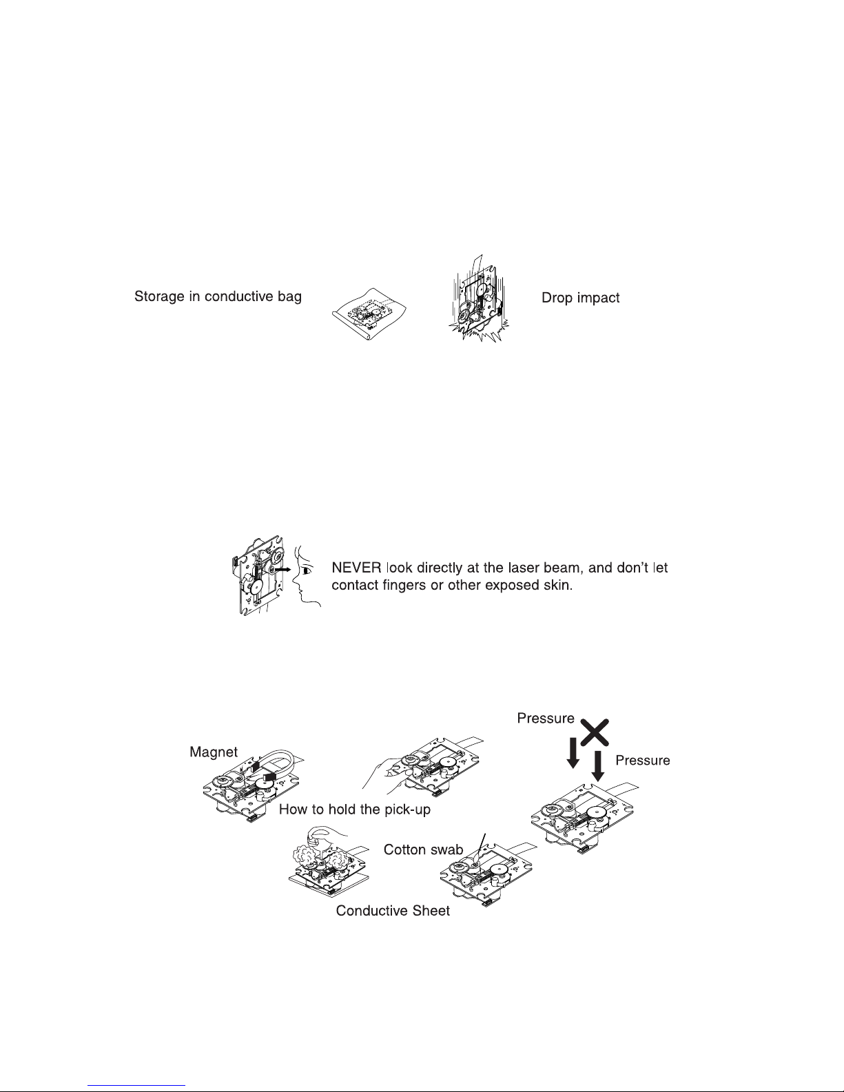
NOTES REGARDING HANDLING OF THE PICK-UP
1. Notes for transport and storage
1) The pick-up should always be left in its conductive bag until immediately prior to use.
2) The pick-up should never be subjected to external pressure or impact.
2. Repair notes
1) The pick-up incorporates a strong magnet, and so should never be brought close to magnetic materials.
2) The pick-up should always be handled correctly and carefully, taking care to avoid external pressure and
impact. If it is subjected to strong pressure or impact, the result may be an operational malfunction and/or
damage to the printed-circuit board.
3) Each and every pick-up is already individually adjusted to a high degree of precision, and for that reason
the adjustment point and installation screws should absolutely never be touched.
4) Laser beams may damage the eyes!
Absolutely never permit laser beams to enter the eyes!
Also NEVER switch ON the power to the laser output part (lens, etc.) of the pick-up if it is damaged.
5) Cleaning the lens surface
If there is dust on the lens surface, the dust should be cleaned away by using an air bush (such as used
for camera lens). The lens is held by a delicate spring. When cleaning the lens surface, therefore, a cotton
swab should be used, taking care not to distort this.
6) Never attempt to disassemble the pick-up.
Spring by excess pressure. If the lens is extremely dirty, apply isopropyl alcohol to the cotton swab. (Do not
use any other liquid cleaners, because they will damage the lens.) Take care not to use too much of this
alcohol on the swab, and do not allow the alcohol to get inside the pick-up.
SERVICING PRECAUTIONS
SECTION 1 GENERAL
1-3
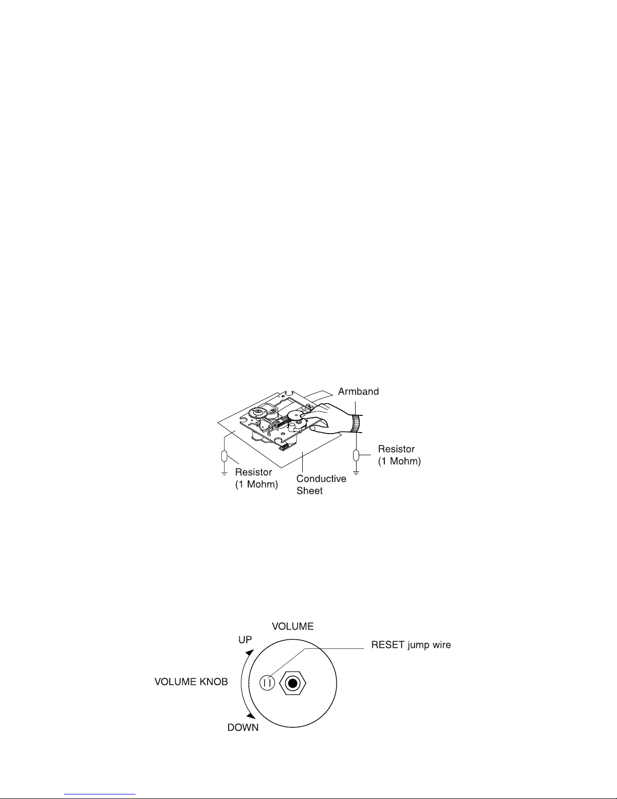
NOTES REGARDING COMPACT DISC PLAYER REPAIRS
1. Preparations
1) Compact disc players incorporate a great many ICs as well as the pick-up (laser diode). These components
are sensitive to, and easily affected by, static electricity. If such static electricity is high voltage, components
can be damaged, and for that reason components should be handled with care.
2) The pick-up is composed of many optical components and other high-precision components. Care must be
taken, therefore, to avoid repair or storage where the temperature of humidity is high, where strong
magnetism is present, or where there is excessive dust.
2. Notes for repair
1) Before replacing a component part, first disconnect the power supply lead wire from the unit
2) All equipment, measuring instruments and tools must be grounded.
3) The workbench should be covered with a conductive sheet and grounded.
When removing the laser pick-up from its conductive bag, do not place the pick-up on the bag. (This is
because there is the possibility of damage by static electricity.)
4) To prevent AC leakage, the metal part of the soldering iron should be grounded.
5) Workers should be grounded by an armband (1MΩ)
6) Care should be taken not to permit the laser pick-up to come in contact with clothing, in order to prevent
static electricity changes in the clothing to escape from the armband.
7) The laser beam from the pick-up should NEVER be directly facing the eyes or bare skin.
CLEARING MALFUNCTION
You can reset your unit to initial status if malfunction occur(button malfunction, display, etc.).
Using a pointed good conductor(such as driver), simply short the RESET jump wire on the inside of
the volume knob for more than 3 seconds.
If you reset your unit, you must reenter all its settings(stations, clock, timer)
NOTE: 1. To operate the RESET jump wire, pull the volume rotary knob and release it.
2. If you wish to operate the RESET jump wire, it is necessary to unplug the power cord.
1-4
ESD PRECAUTIONS
Electrostatically Sensitive Devices (ESD)
Some semiconductor (solid state) devices can be damaged easily by static electricity. Such components
commonly are called electrostatically sensitive devices (ESD). Examples of typical ESD devices are
integrated circuits and some field-effect transistors and semiconductor chip components. The following
techniques should be used to help reduce the incidence of component damage caused by static electricity.
1. Immediately before handling any semiconductor component or semiconductor-equipped assembly, drain
off any electrostatic charge on your body by touching a know earth ground. Alternatively, obtain and
wear a commercially available discharging wrist strap device, which should be removed for potential
shock reasons prior to applying power to the unit under test.
2. After removing an electrical assembly equipped with ESD devices, place the assembly on a conductive
surface such as aluminum foil, to prevent electrostatic charge buildup or exposure of the assembly.
3. Use only a grounded-tip soldering iron to solder or unsolder ESD devices.
4. Use only an anti-static solder removal device. Some solder removal devices not classified as "anti-static"
can generate electrical charges sufficient to damage ESD devices.
5. Do not use freon-propelled chemicals These can generate electrical charges sufficient to damage ESD
devices.
6. Do not remove a replacement ESD device from its protective package until immediately before you are
ready to install it. (Most replacement ESD devices are packaged with leads electrically shorted together
by conductive foam, aluminum foil or comparable conductive materials).
7. Immediately before removing the protective material from the leads of a replacement ESD device, touch
the protective material to the chassis or circuit assembly into which the device will by installed.
CAUTION : BE SURE NO POWER IS APPLIED TO THE CHASSIS OR CIRCUIT, AND OBSERVE ALL
OTHER SAFETY PRECAUTIONS.
8. Minimize bodily motions when handing unpackaged replacement ESD devices. (Otherwise harmless
motion such as the brushing together of your clothes fabric or the lifting of your foot from a carpeted floor
can generate static electricity sufficient to damage an ESD device).
[CAUTION. GRAPHIC SYMBOLS]
THE LIGHTNING FLASH WITH ARROWHEAD SYMBOL. WITHIN AN EQUILATERAL
TRIANGLE, IS INTENDED TO ALERT THE SERVICE PERSONNEL TO THE PRESENCE
OF UNINSULATED "DANGEROUS VOLTAGE" THAT MAY BE OF SUFFICIENT
MAGNITUDE TO CONSTITUTE A RISK OF ELECTRIC SHOCK.
THE EXCLAMATION POINT WITHIN AN EQUILATERAL TRIANGLE IS INTENED TO
ALERT THE SERVICE PERSONNEL TO THE PRESENCE OF IMPORTANT SAFETY
INFORMATION IN SERVICE LITERATURE.
1-5
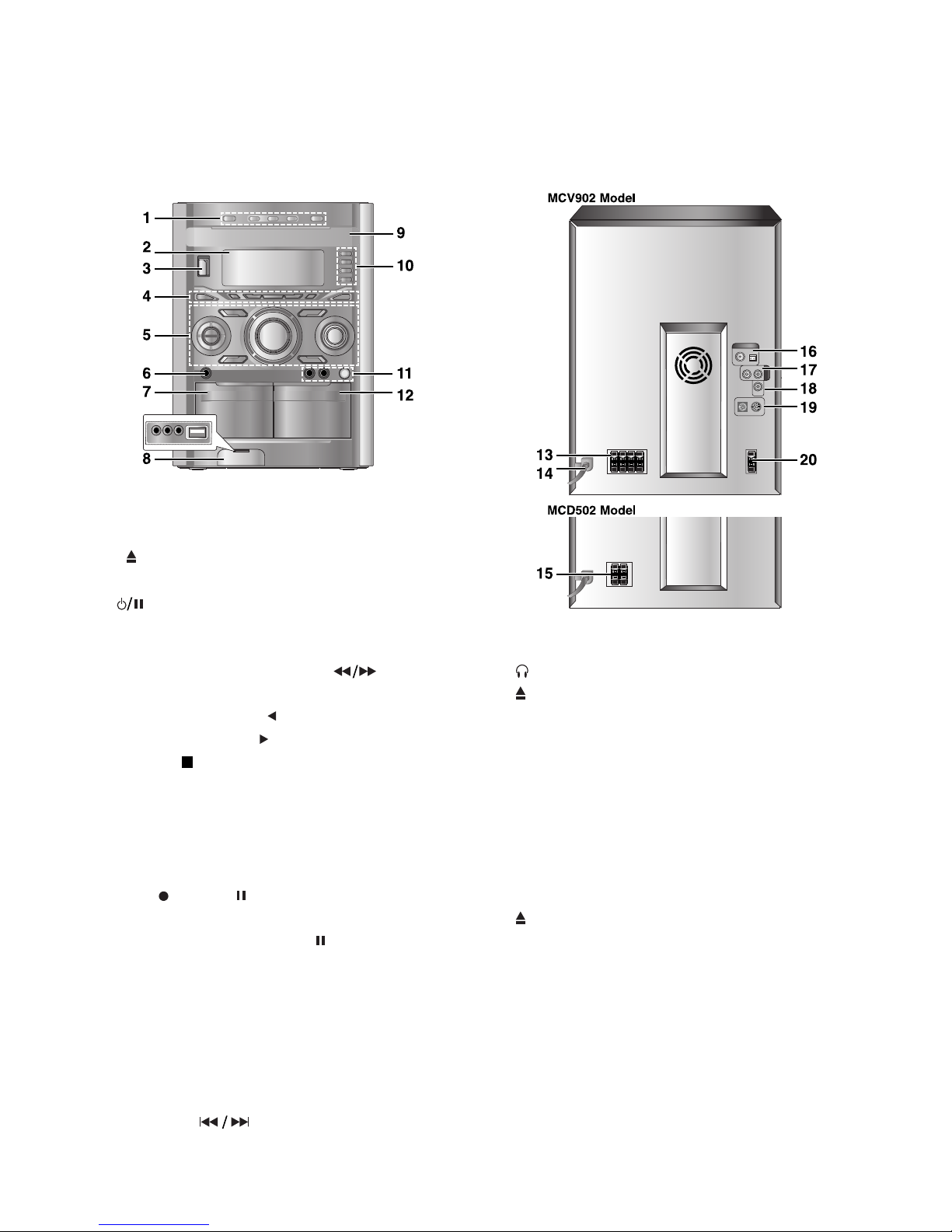
LOCATION OF USERS CONTROLS
FRONT / BACK PANEL
1. • DISC SKIP button
• CD SELECT buttons (DISC1, DISC2, DISC3)
• OPEN/CLOSE button
2. DISPLAY WINDOW
3. (POWER) button
4. • XDSS button
• AUTO TUNING DOWN/UP button
REWIND / FAST FORWARD ( ) button
• PRESET DOWN/UP button
BACKWARD PLAY ( ) button : OPTIONAL
FORWARD PLAY ( ) button
• STOP ( ) / CLEAR button
• OAO button
5. • FUNCTION SELECT buttons
[TUNER, TAPE, CD, AUX / AV, USB]
• PLAY MODE/ DEMO button
• PROG. MEMO. button
• REC / PAUSE (RECORD/ RECORD
PAUSE) button
• SET/ RDS(OPTIONAL)/ CD[ ]/ AM-NOISE button
• VOLUME CONTROL KNOB
• EQ button
• SURROUND button
• USER EQ button
• MP3 OPT (MP3 OPTIMIZER) button
• MULTI JOG
MANUAL TUNING
CD SKIP ( )
CLOCK ADJUST
6. PHONES (HEADPHONE JACK) : ø6.3mm
7. PUSH EJECT position - TAPE 1
8. • GAME LINK connector (VIDEO IN, AUDIO L/R)
• USB connector
9. CD DOOR
10.CLOCK button
• TIMER button
• ST./ MONO/ NOR. DUBB. button
• CD SYNC./ HI-DUBB. button
11.• MIC1/ MIC2 (MIC JACK) : ø6.3 mm - OPTIONAL
• MIC VOL. (MIC VOLUME KNOB) - OPTIONAL
12. PUSH EJECT position - TAPE 2
13.SPEAKER TERMINAL (MCV902 model)
14.POWER CORD
15.SPEAKER TERMINAL (MCD502 model)
16.AM/ FM ANTENNA TERMINAL
17.AUX IN (AUXILIARY INPUT connector)
18.VIDEO OUT connector
19.WOOFER SYSTEM connector (MCV902 model)
20.SUB WOOFER SPEAKER TERMINAL
(MCV902 model)
1-6
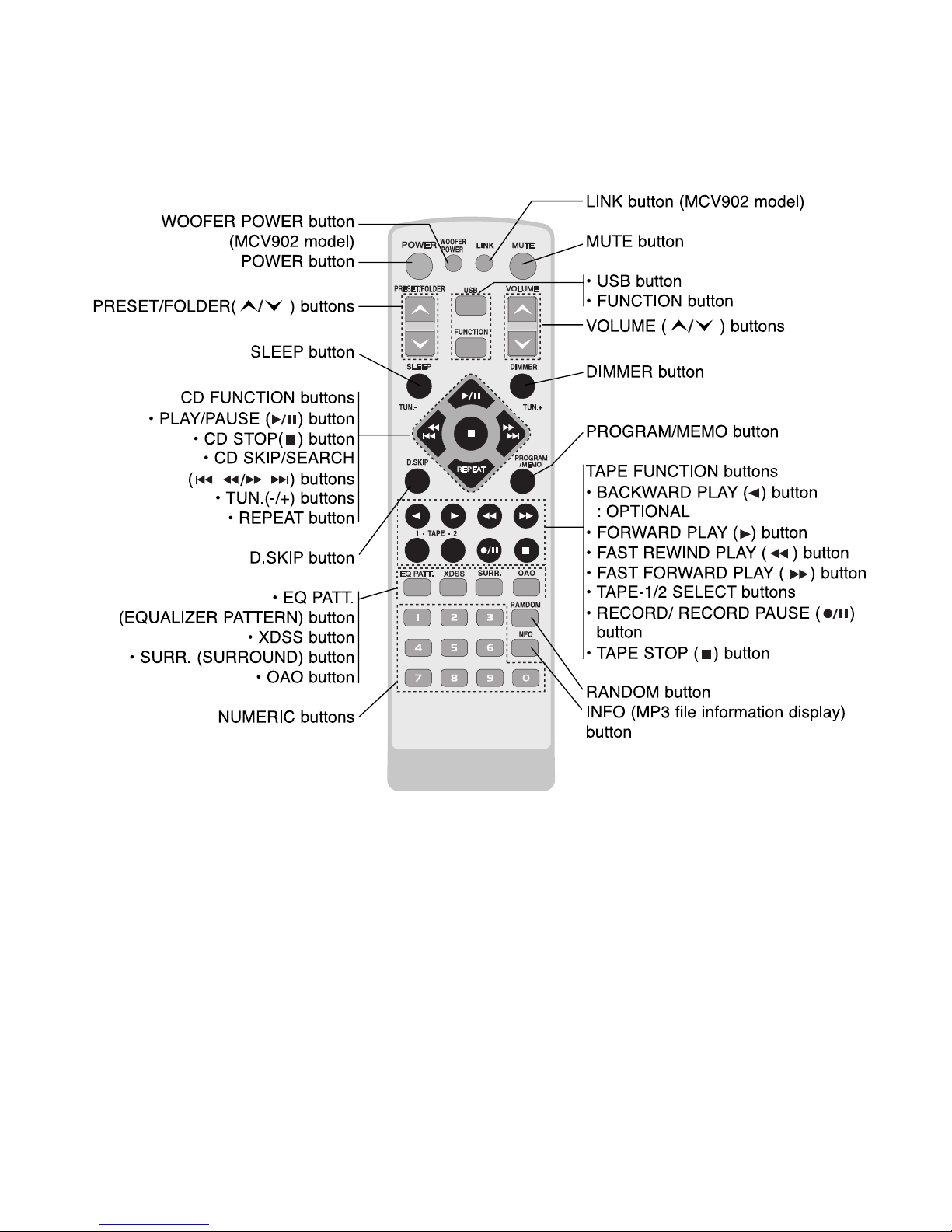
REMOTE CONTROL

1-7
SPECIFICATIONS
MODEL
MCV902 MCD502
SECTION
Power supply Refer to the back panel of the unit.
Power consumption Refer to the back panel of the unit.
[GENERAL]
Net weight 8.45kg 8kg
External dimensions (WxHxD) 280 X 365 X 370mm
Frequency response 40 ~ 20000Hz
[CD] Signal-to-noise ratio 75dB
Dynamic range 80dB
Tuning range 87.5 ~ 108.0MHz or 65 ~ 74MHz, 87.5 ~ 108.0MHz
Intermediate frequency 10.7MHz
Signal to noise ratio 60/55dB
[TUNER]
Frequency response 140 ~ 10000Hz
Tuning range 522 ~ 1620 kHz or 520 ~ 1720kHz
Intermediate frequency 450kHz
Signal to noise ratio 30dB
Frequency response 140 ~ 1800Hz
Front : 270W + 270W (MCV902 Model)
Output power
250W + 250W (MCV502 Model)
Surround : 110W + 110W (MCV902 Model)
[AMP] Subwoofer : 175W + 175W (MCV902 Model)
T.H.D 0.7%
Frequency response 42 ~ 20000Hz
Signal-to-noise ratio 75dB
Ta pe speed 3000 3% (MTT-111. NORMAL-SPEED)
Wow flutter 0.25% (MTT -111, JIS-WTD)
F.F/REW Time 120sec (C-60)
[TAPE] Frequency response 125 ~ 8000Hz
Signal to noise ratio 43dB
Channel separation 50dB (P/B) / 45dB (R/P)
Erase ratio 55dB (MTT-5511)
Speaker name
Front speaker (L/R) Surround speaker (L/R)
MCS902F / MCS502F MCS902S
Type Bass reflex 2 way 2 speaker Bass reflex 2 way 2 speaker
Impedance 6Ω 24Ω
Frequency response 60 ~ 20000Hz 70 ~ 20000Hz
[Speakers] Sound rressure level 86dB/W (1m) 83dB/W (1m)
Rated input power 270W / 250W 110W
Max. input power 540W / 500W 220W
Net dimensions (W x H x D) 272 x 455 x 320mm 210 x 450 x 280mm
Net weight (1EA) 9.17kg 4.62kg
Speaker name MCS902AW MCS902W
Type 1 way 1 speaker 1 way 1 speaker
Impedance 12Ω 12Ω
Frequency response 55 ~ 1500Hz 55 ~ 1500Hz
[Subwoofer] Sound pressure level 85dB/W (1m) 85dB/W (1m)
Rated input power 175W 175W
Max. input power 350W 350W
Net dimensions (W x H x D) 273 x 370 x 322mm 273 x 370 x 322mm
Net weight (1EA) 7.3kg 7.3kg
* Design and specifications are subject to change prior notice.
FM
AM
(MW)

1-8
MEMO
283
A56
450
301
453
A41
A26
A46
275
450
250
255
288
265
259
268
260
450
450
450
454
248
283
450
450
302
266
265
292
450
450
450
450
261
293
274
274
269
271
289
277
276
454
281
451
282
A43
A00
A46
A47
A52
A51
453
456
450
450
450
291
270
303
452
450
450
450
450
279
280
454
454
305
455
278
285
454
457
FAN
450
CABLE2
CABLE1
CD
MAIN
FRONT
SMPS
SUB
SVC purchase order caution
MAIN board is array coming USB board.
Purchase order board separately supply
incomprehensible.
Supply is possible in Location No A46
state in exploded views.
CABLE5
CABLE6
2-1 2-2
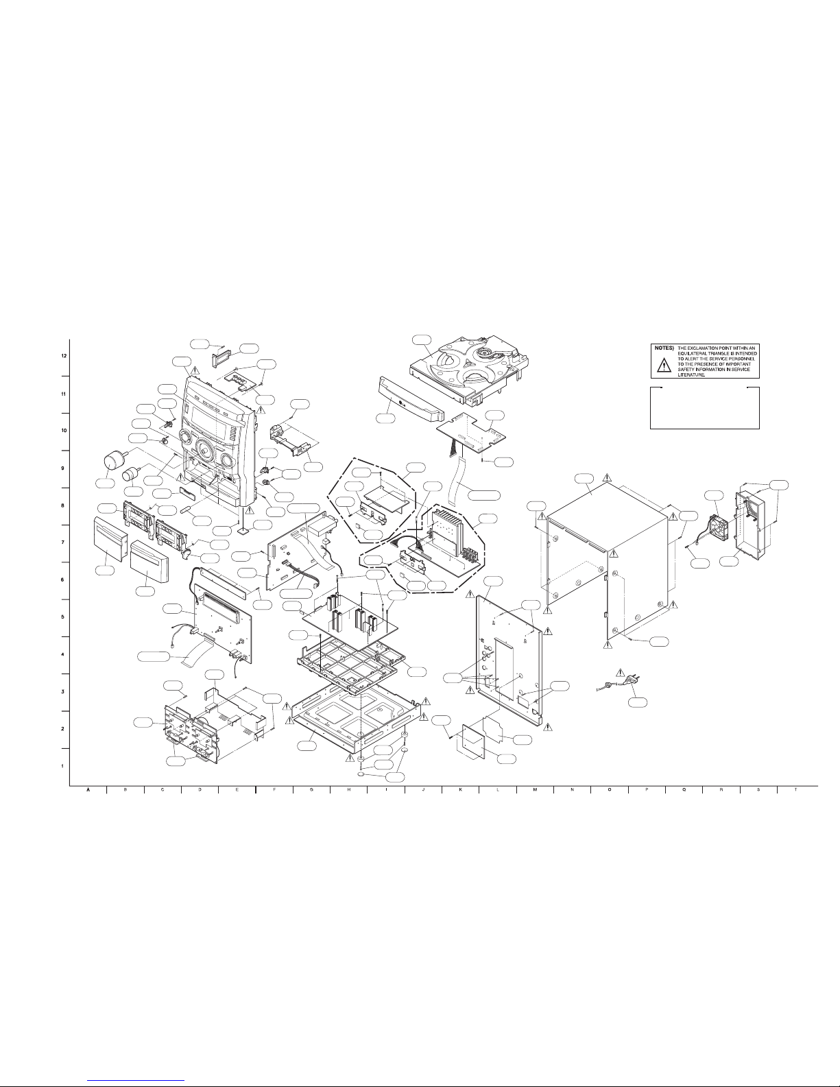
SECTION 2 EXPLODED VIEWS
CABINET EXPLODED VIEW

023
015
022
019
037
021
020
018
017
006
A01
008
007
001
002
003
009
009
011
013
A02
025
2-3 2-4
TAPE DECK MECHANISM EXPLODED VIEW
1. TAPE DECK MECHANISM (A/R & A/S : A/R DECK)

2-5 2-6
016
018
007
008
015
019
021
020
017
A03
009
003
011
013
009
022
025
023
2. TAPE DECK MECHANISM (A/R & A/S : A/S DECK)

2-7 2-8
416
151
159
165
164
417
166
417
167
416
177
175
172
170
419
417
418
418
190
189
188
A30
A32
A26
181
187
186
184
421
421
185
156
155
153
173
168
163
162
441
440
422
A35
417
CD MECHANISM EXPLODED VIEW

2-9 2-10
A80BL
A80L
A80A
858
857
856
855
854
851
850
852
853
860
859
857
862
WIRE81
861
A80BR
A80R
A80A
858
857
856
855
854
851
850
852
853
860
859
857
862
WIRE80
861
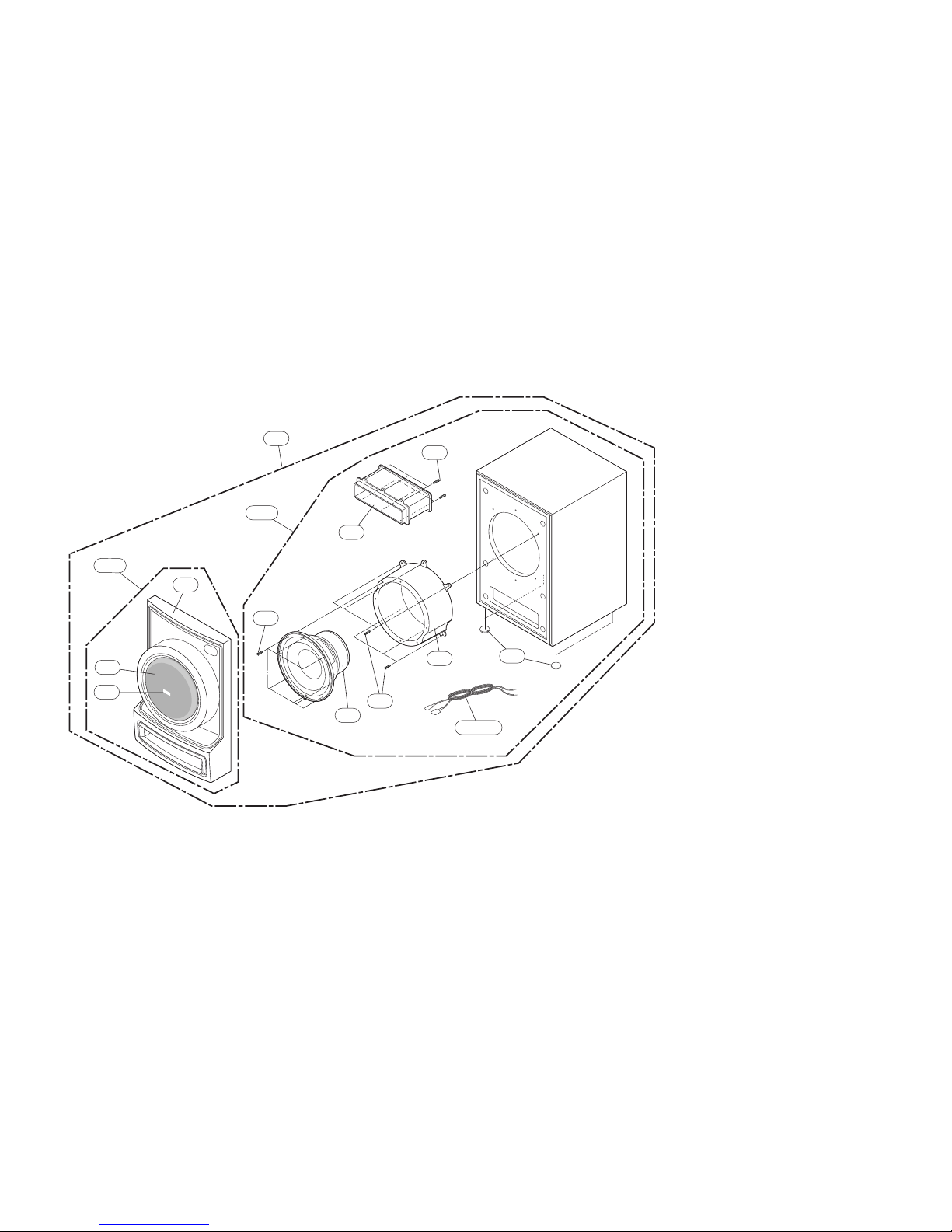
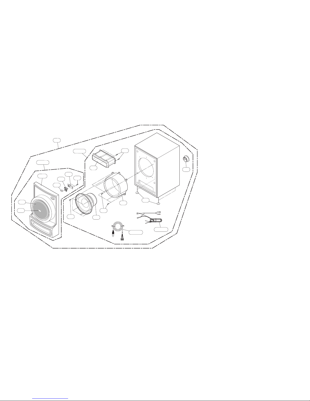
SPEAKER EXPLODED VIEW
1. MODEL : MCS902F

2-11 2-12
A60BR
A60R
A60A
WIRE60
659
658
660
656
657
655
654
651
650
652
653
661
662
A60BL
A60L
A60A
WIRE61
659
658
660
656
657
655
654
651
650
652
653
661
662
2. MODEL : MCS902S
2-13 2-14
A90A
A90B
WIRE92
959
958
957
960
951
952
950
A91
961
962
958
3. MODEL : MCS902W
2-15 2-16
A90AW
A90BW
950A
WIRE91
WIRE90
953
954
955
956
963
958
959
957
951
952
A90
961
962
958
960
4. MODEL : MCS902AW
2-17
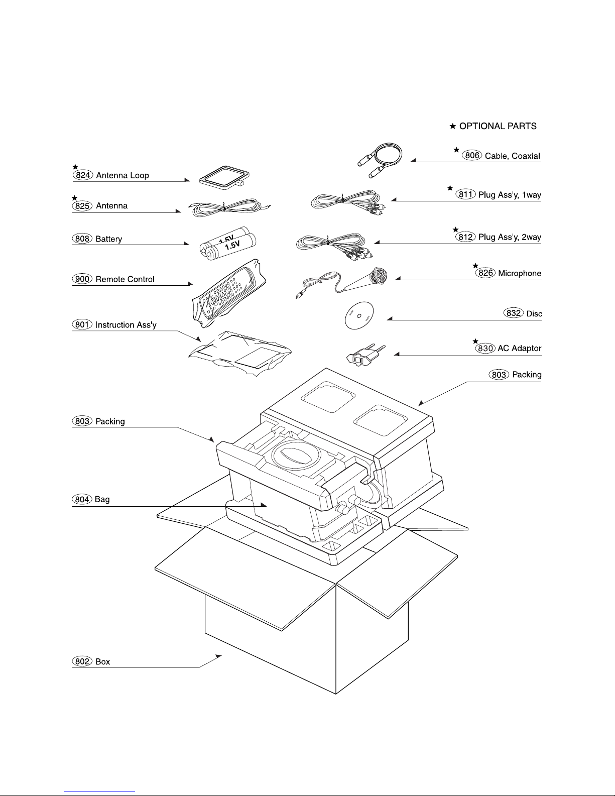
PACKING ACCESSORY VIEW

3-1
ELECTRICAL TROUBLESHOOTING GUIDE
SECTION 3 AUDIO PART ELECTRICAL
1. POWER (SMPS)
NO POWER
CHECK AC
LINE PATTERN
CONNECT
THE OPEN LINE
CHECK F901 FUSE REPLACE FUSE
CHECK BD901 + TO
- PIN IMPEDANCE
LOW IMPEDANCE
CHANGE ASSY
CHECK C986
VOLT(5.6V)
CHECK LINE SHORT
CHECK CONNECTION
CN902, CN903
NO SOUND
INSERT POWER CORD
AFTER 10 SECONDS
CHECK THE AMP
MODULE SHORT
CHECK C961, C951
VOLT (OVER 40V)
CHANGE
FR971, 972, 974, 975
CHECK C958, C968
VOLT (OVER 9V)
PORTECTION CHECK NO SOUND LISTS
DISPLAY INSERT POWER
CORD AFTER 1 MINUTE
3-2
2. P-SENS
P-SENS PART
YES
YES
SMPS ASS'Y CN902
- -> 7PIN 5.1V CHECK
SMPS TROUBLESHOOTING CONSULT
NO
YES
MAIN PCB CN710
7PIN 5.1V CHECK
CN710 CONNECTION STATE CHECK
NO
YES
MAIN PCB CN304
6PIN 5.1V CHECK
MAIN PCB PATTERN CUTTING
AND SHORT CHECK
IC304 KIA7042 CHANGEµ-COM IC302 1PIN 4.4V CHECK
NO
YES
FRONT PN304 35 PIN 5.1V CHECK
YES YES
FRONT IC304(RESET IC)
STATE CHECK
IC304 INPUT VOLTAGE 5V OVER
STATE CHECK AND OUTPUT VOLTAGE 4V
OVER STATE CHECK
NO
3. VKK CHECK
VKK CHECK
YES
YES
CN710 10PIN DC
-32V CHECK
SMPS TROUBLESHOOTING CONSULT
NO
IC301 50PIN VOLTAGE CHECK

3-3
5. P-CTRL CHECK
P-CTRL CHECK
YES
YES
PN304 32PIN
"P-CTRL" CHECK (HIGH)
MICOM IC302 STATE CHECK
YES
CN710 5PIN CHECK
SMPS + MAIN BORD-TO-BORD CHECK
NO
NO
SMPS TROUBLESHOOTING CONSULT
4. MICOM (IC302) CHANGE
MICOM (IC302)
CHANGE
IC302 CHANGE
"RESET"
IC302
10PIN CHECK(LOW
--> HIGH)
Q302, Q303
STATE CHECK
NO NO
YES
YES YES
YES
"P-SENS"
CHECK
NO
P-SENS
TROUBLESHOOTING
CONSULT
X301, X302 CHANGE
TR "Q302, Q303"
CHANGE
IC302 VDD
(19, 20, 59) PIN
VOLTAGE
CHECK
PN304 34PIN
+5.6V (MI) CHECK
NO NO NO
YES
X301:9.8304MHz,
X302:32.768KHz
VIBRATION SIGNAL
CHECK
NO
YES
YES
MAIN CN710
6PIN CHECK
SMPS
TROUBLESHOOTI
NG CONSULT
 Loading...