

Page 1

- 1-1 -
[CONTENTS]
❍ SECTION 1. GENERAL
• SERVICING PRECAUTIONS
.....................................................................................................
1-2
• ESD PRECAUTIONS
.................................................................................................................
1-4
• SPECIFICATION
........................................................................................................................
1-5
❍ SECTION 2. TROUBLESHOOTING
• ADJUSTMENTS
.........................................................................................................................
2-1
• TROUBLESHOOTING ............................................................................................................... 2-2
• WAVEFORMS OF MAJOR CHECK POINT............................................................................. 2-11
• BLOCK DIAGRAM
....................................................................................................................
2-21
• SCHEMATIC DIAGRAMS
........................................................................................................
2-23
• WIREING DIAGRAM ................................................................................................................ 2-29
• PRINTED CIRCUIT DIAGRAMS .............................................................................................. 2-31
• INTERNAL BLOCK DIAGRAM OF ICs .................................................................................... 2-38
❍ SECTION 3. EXPLODED VIEWS
• CABINET AND MAIN FRAME SECTION
...................................................................................
3-1
❍ SECTION 4. SPEAKER PART
• SPEAKER PART
........................................................................................................................
4-1
❍ SECTION 5. REPLACEMENT PARTS LIST
• REPLACEMENT PARTS LIST
....................................................................................................
5-1
Page 2

❏ SERVICING PRECAUTIONS
NOTES REGARDING HANDLING OF THE PICK-UP
1. Notes for transport and storage
1) The pick-up should always be left in its conductive bag until immediately prior to use.
2) The pick-up should never be subjected to external pressure or impact.
2. Repair notes
1) The pick-up incorporates a strong magnet, and so should never be brought close to magnetic materials.
2) The pick-up should always be handled correctly and carefully, taking care to avoid external pressure and
impact. If it is subjected to strong pressure or impact, the result may be an operational malfunction and/or
damage to the printed-circuit board.
3) Each and every pick-up is already individually adjusted to a high degree of precision, and for that reason
the adjustment point and installation screws should absolutely never be touched.
4) Laser beams may damage the eyes!
Absolutely never permit laser beams to enter the eyes!
Also NEVER switch ON the power to the laser output part (lens, etc.) of the pick-up if it is damaged.
5) Cleaning the lens surface
If there is dust on the lens surface, the dust should be cleaned away by using an air bush (such as used
for camera lens). The lens is held by a delicate spring. When cleaning the lens surface, therefore, a
cotton swab should be used, taking care not to distort this.
6) Never attempt to disassemble the pick-up.
Spring by excess pressure. If the lens is extremely dirty, apply isopropyl alcohol to the cotton swab. (Do
not use any other liquid cleaners, because they will damage the lens.) Take care not to use too much of
this alcohol on the swab, and do not allow the alcohol to get inside the pick-up.
- 1-2 -
Storage in conductive bag
Drop impact
NEVER look directly at the laser beam, and don’t let
contact fingers or other exposed skin.
Magnet
How to hold the pick-up
Pressure
Pressure
Cotton swab
Conductive Sheet
SECTION 1. GENERAL
Page 3
NOTES REGARDING COMPACT DISC PLAYER REPAIRS
1. Preparations
1) Compact disc players incorporate a great many ICs as well as the pick-up (laser diode). These
components are sensitive to, and easily affected by, static electricity. If such static electricity is high
voltage, components can be damaged, and for that reason components should be handled with care.
2) The pick-up is composed of many optical components and other high-precision components. Care must
be taken, therefore, to avoid repair or storage where the temperature of humidity is high, where strong
magnetism is present, or where there is excessive dust.
2. Notes for repair
1) Before replacing a component part, first disconnect the power supply lead wire from the unit
2) All equipment, measuring instruments and tools must be grounded.
3) The workbench should be covered with a conductive sheet and grounded.
When removing the laser pick-up from its conductive bag, do not place the pick-up on the bag. (This is
because there is the possibility of damage by static electricity.)
4) To prevent AC leakage, the metal part of the soldering iron should be grounded.
5) Workers should be grounded by an armband (1MΩ)
6) Care should be taken not to permit the laser pick-up to come in contact with clothing, in order to prevent
static electricity changes in the clothing to escape from the armband.
7) The laser beam from the pick-up should NEVER be directly facing the eyes or bare skin.
CLEARING MALFUNCTION
You can reset your unit to initial status if malfunction occur(button malfunction, display, etc.).
Using a pointed good conductor(such as driver), simply short the RESET jump wire on the inside of the
volume knob for more than 3 seconds.
If you reset your unit, you must reenter all its settings(stations, clock, timer)
NOTE: 1. To operate the RESET jump wire, pull the volume rotary knob and release it.
2. If you wish to operate the RESET jump wire, it is necessary to unplug the power cord.
- 1-3 -
Armband
Conductive
Sheet
Resistor
(1 Mohm)
Resistor
(1 Mohm)
VOLUME KNOB
UP
DOWN
VOLUME
RESET jump wire
Page 4

❐ ESD PRECAUTIONS
Electrostatically Sensitive Devices (ESD)
Some semiconductor (solid state) devices can be damaged easily by static electricity. Such components
commonly are called Electrostatically Sensitive Devices (ESD). Examples of typical ESD devices are integrated
circuits and some field-effect transistors and semiconductor chip components. The following techniques should
be used to help reduce the incidence of component damage caused by static electricity.
1. Immediately before handling any semiconductor component or semiconductor-equipped assembly, drain off
any electrostatic charge on your body by touching a known earth ground. Alternatively, obtain and wear a
commercially available discharging wrist strap device, which should be removed for potential shock reasons
prior to applying power to the unit under test.
2. After removing an electrical assembly equipped with ESD devices, place the assembly on a conductive
surface such as aluminum foil, to prevent electrostatic charge buildup or exposure of the assembly.
3. Use only a grounded-tip soldering iron to solder or unsolder ESD devices.
4. Use only an anti-static solder removal device. Some solder removal devices not classified as "anti-static" can
generate electrical charges sufficient to damage ESD devices.
5. Do not use freon-propelled chemicals. These can generate electrical charges sufficient to damage ESD
devices.
6. Do not remove a replacement ESD device from its protective package until immediately before you are ready
to install it. (Most replacement ESD devices are packaged with leads electrically shorted together by
conductive foam, aluminum foil or comparable conductive materials).
7. Immediately before removing the protective material from the leads of a replacement ESD device, touch the
protective material to the chassis or circuit assembly into which the device will by installed.
CAUTION : BE SURE NO POWER IS APPLIED TO THE CHASSIS OR CIRCUIT, AND OBSERVE ALL OTHER
SAFETY PRECAUTIONS.
8. Minimize bodily motions when handing unpackaged replacement ESD devices. (Otherwise harmless motion
such as the brushing together of your clothes fabric or the lifting of your foot from a carpeted floor can
generate static electricity sufficient to damage an ESD device).
[CAUTION. GRAPHIC SYMBOLS]
- 1-4 -
THE LIGHTNING FLASH WITH APROWHEAD SYMBOL. WITHIN AN EQUILATERAL
TRIANGLE, IS INTENDED TO ALERT THE SERVICE PERSONNEL TO THE PRESENCE
OF UNINSULATED “DANGEROUS VOLTAGE” THAT MAY BE OF SUFFICIENT
MAGNITUDE TO CONSTITUTE A RISK OF ELECTRIC SHOCK.
THE EXCLAMATION POINT WITHIN AN EQUILATERAL TRIANGLE IS INTENDED TO
ALERT THE SERVICE PERSONNEL TO THE PRESENCE OF IMPORTANT SAFETY
INFORMATION IN SERVICE LITERATURE.
Page 5

❏ SPECIFICATIONS
- 1-5 -
SECTION SPECIFICATION
General Power supply Refer to the back panel of the unit
Power consumption 65W
Extemal dimensions(W X H X D)
161 X 255 X 268mm
CD Frequency Response 40 -18000Hz
Signal-to-noise ratio 70dB
Dynamic range 70dB
Tuning Range 87.5 -108.0MHz
Intermediate Frequency 10.7 MHz
FM Signal-to-noise ratio 60/55dB
Frequency Response 60 - 10000Hz
Tuning Range 522 - 1611kHz or 530 - 1610kHz
AM Intermediate Frequency 450kHz
Signal-to-noise ratio 35dB
Frequency Response 100 -1800 Hz
AMP Output Power 30W + 30W
T.H.D 0.15%
Frequency Response 40-25000Hz
Signal-to-noise ratio 80dB
TAPE Tape Speed 4.75cm/sec
Wow Flutter 0.25% (MTT-111,JIS-WTD)
F.F/REW Time 120sec(C-60)
Frequency Response 250-8000Hz
Signal-to-noise ratio 43dB
Channel Separation 50dB(P/B)/45dB(R/P)
Erase Ratio 55dB (MTT-5511)
Speaker MODEL LXS-M335
Type 2 Way 2 Speaker
Impedance 6Ω
Frequency Response 80-20000Hz
Sound Pressure Level 87dB/W(1m)
Rated Input Power 30W
Max.Input Power 60W
Net Dimension(W X H X D) 160 X 248 X 200mm
NOTE : Specification are subject to change without notice in the course of product improvement.
TUNER
Page 6

- 1-6 -
MEMO
Page 7

- 2-1 -
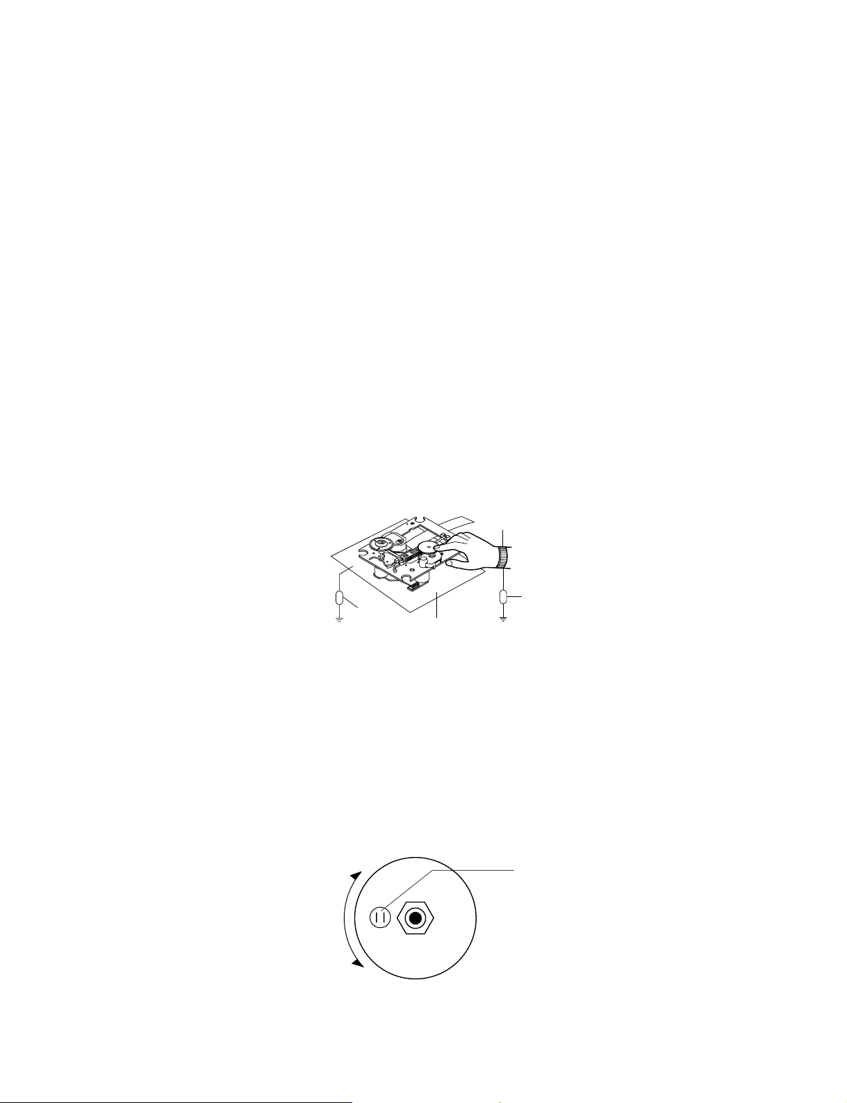
TAPE DECK ADJUSTMENT
1. AZIMUTH ADJUSTMENT
Figure 1. Azimuth Adjustment Connection Diagram
CH1 CH2
Speaker Out
Playback Mode
Head
Test Tape
MTT-114
L ch
R ch
GND
Dual-trace
synchroscope
Electronic
Voltmeter
L out
R out
Unit
❏ ADJUSTMENTS
This set has been aligned at the factory and normally will not require further adjustment. As a result, it is not
recommended that any attempt is made to modificate any circuit. If any parts are replaced or if anyone tampers
with the adjustment, realignment may be necessary.
IMPORTANT
1. Check Power-source voltage.
2. Set the function switch to band being aligned.
3. Turn volume control to minimum unless otherwise noted.
4. Connect low side of signal source and output indicator to chassis ground unless otherwise specified.
5. Keep the signal input as low as possible to avoid AGC and AC action.
Deck Mode Test Tape Test Point Adjustment Adjust for
Palyback MTT-114 Speaker Out
DECK Screw
Maximum
Azimuth Screw
SECTION 2. ELECTRICAL SECTION
Page 8

- 2-2 -
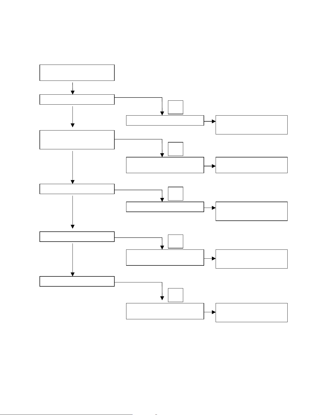
❏ TROUBLESHOOTING
• CD PART
TURN ON CD
OPEN CLOSE CHECK
CONNECTOR CHECK ( PN508,PN507 )
CHECK POWER SUPPLY CIRCUIT( PN508 )
CHECK MICOM INTERFACE CIRCUIT( PN507 )
CHECK MICOM INTERFACE CIRCUIT( PN507 )
CONNECTOR CHECK(PN501,PN503)
CHECK PICKUP MOVEMENT
CHECK BA5810FP (IC503)
CHECK MN6627933CG (IC501)
CHECK AN22004 (IC502)
CONNECTOR CHECK (PN508)
CONNECTOR CHECK
( PN508,PN507,PN503,PN501 )
“ READING ”
DISPLAY CHECK
READING OK CHECK
IF PLAY, AUDIO
OUTPUT CHECK
OK
YES
NO
NO
NO
NO
NO
NO
NO
NO
NO
NO
NO
YES
YES
YES
Page 9

- 2-3 -
DEFECTIVE MAIN
POEWR SUPPLY
DEFECTIVE MICOM
DEFECTIVE IC503
DEFECTIVE MICOM
MECHANISM
• OPEN CLOSE NG
CONNECTOR LOCKING CHECK ( PN508,PN507 )
CHECK POWER SUPPLY CIRCUIT( PN508
,PN507) PN 508 PIN 8 = 6.2V, PIN 7 = 5V
PN507 PIN 1 = 5V
CHECK VOLTAGE CHANGE OF OPEN CLOSE,
AND BTLMUTE VOLTAGE(= 5V)
(PN507 PIN 12:OPEN, 13:CLOSE, 14:BTLMUTE)
CHECK VOLTAGE CHANGE LO+, LO- OF IC503
(PN507, PIN OPEN:12, CLOSE:13)
NO
NO
NO
NO
YES
YES
YES
Page 10

- 2-4 -
• “ READING ” DISPLAY CHECK (= ONLY “CD “DISPLAY)
CONNECTOR LOCKING CHECK
(PN508,PN507,PN503,PN501 )
CHECK VOLTAGE THE PIN 2 OF
IC505 PIN2 : 3.3V
CHECK RESET SIGNAL OF PN507
PN507 PIN7 : 5V
CHECK MICOM INTERFACE
CIRCUIT( PN507 )
PN507 PIN 6,8,9,10 SIGNAL CHECK
(6: STAT, 8: MDATA, 9:MCLK, 10:MLD)
CHECK THE WAVE FORM #1
CHECK POWER SUPPLY
PORT( PN508 ,PN507)
PN508 PIN 8 = 6.2V, PIN 7 = 5V
PN507 PIN 1 = 5V
DEFECTIVE CONNECTOR OR
MAIN POWER SUPPLAY
DEFECTIVE IC505
DEFECTIVE MICOM OR
CONNECTOR
DEFECTIVE MICOM OR
CONNECTOR
DEFECTIVE IC501
NO
NO
NO
NO
NO
YES
YES
YES
YESYES
Page 11
- 2-5 -
• READING OK CHECK (= “NO DISC” DISPLAY)
AAAA
BBBB
CCCC
DDDD
EEEE
CONNECTOR LOCKING
CHECK(PN501,PN503)
DOES LENSE MOVE ?
(= UP & DOWN)
DOES SLED MOVE ?
CHECK PN503 PIN 3,4( SL+,SL-)
CHECK PN501 PIN 13,16
( FA-, FA+)
DEFECTIVE PICKUP OR
IC503 OR IC501 OR IC502
DEFECTIVE PICKUP OR
IC503 OR IC501
DEFECTIVE PICKUP OR
IC502
DEFECTIVE PICKUP OR
IC503
DEFECTIVE PICKUP OR
IC503 OR IC501 OR IC502
CHECK PN503 PIN 10( LD )
CHECK PN503 PIN
5,6( SP+,SP-)
CHECK PN501 PIN 14,15
(TA- ,TA+)
DOES LASER LIGHT ?
DOES SPINDLE ROTATE ?
IS READING OK ?
NO
NO
NO
NO
NO
NO
NO
NO
NO
NO
YES
YESYES
YES
YES
YES
Page 12
- 2-6 -
• READING OK CHECK #A (= “NO DISC” DISPLAY)
AAAA
DOES SL+ WAVEFORM
APPEAR AT ( IC503 PIN14 AND
PN503 PIN3) WAVEFORM #2
SLED MOTOR WAVE
DOES SLIN WAVEFORM
APPEAR AT ( IC503 PIN 5)
WAVEFORM #2 SLED
DRIVE WAVE
DEFECTIVE IC501
DEFECTIVE IC503
CHECK PN503 CONNECTOR LINE
DEFECTIVE PN503
CONNECTOR
DEFECTIVE PICKUP
SLED MOTOR
NO
NO
NO
NO
NO
YES
YES
Page 13

- 2-7 -
• READING OK CHECK #B (= “NO DISC” DISPLAY)
BBBB
DOES FA+ WAVEFORM
APPEAR AT ( IC503 PIN15 AND
PN501 PIN16) WAVEFORM #3
FOCUS COIL DRIVE WAVE
DOES FAIN- WAVEFORM
APPEAR AT ( IC503 PIN 26)
WAVEFORM #3 FOCUS
DRIVE WAVE
DEFECTIVE IC501
DEFECTIVE IC503
CHECK PN501 CONNECTOR LINE
DEFECTIVE PN501
CONNECTOR
DEFECTIVE PICKUP
FOCUS ACTUATOR
NO
NO
NO
NO
NO
YES
Page 14

- 2-8 -
• READING OK CHECK #C (= “NO DISC” DISPLAY)
CCCC
IS ?V APPLIED TO PIN10 OF PN501
LASER SUPPLY VOLTAGE CHECK
IS 3.3 V APPLIED TO
PIN3 OF IC502
RF IC SUPPLY VOLTAGE
CHECK
IS 2.0 V PIN2 OF IC502
LASER CONTROL
VOLTAGE CHECK
DEFECTIVE IC505
DEFECTIVE IC502
CHECK PN501 CONNECTOR LINE
DEFECTIVE Q501 OR
D502
DEFECTIVE PN501
CONNECTOR
DEFECTIVE PICKUP
LASER PART
NO
NO
NO
NO
NO
NO
YES
YES
Page 15

- 2-9 -
• READING OK CHECK #D (= “NO DISC” DISPLAY)
DDDD
CHECK PN503 CONNECTOR LINE
DEFECTIVE IC501
DEFECTIVE IC503
DEFECTIVE PN503
CONNECTOR
DEFECTIVE PICKUP
“SPINDLE MOTOR
NO
NO
NO
NO
NO
YES
YES
DOES SPIN WAVEFORM
APPEAR AT
( IC503 PIN 6)
WAVEFORM #4
SPINDLE DRIVE WAVE
DOES SP+ WAVEFORM APPEAR
AT ( IC503 PIN12 AND PN503 PIN6)
WAVEFORM #4
SPINDLE MOTOR DRIVE WAVE
Page 16

- 2-10 -
• READING OK CHECK #E (= “NO DISC” DISPLAY)
EEEE
DOES TA+ WAVEFORM APPEAR
AT ( IC503 PIN17 AND PN503 PIN15)
WAVEFORM #5
TRACKING COIL DRIVE WAVE
DOES TAIN- WAVEFORM
APPEAR AT
( IC503 PIN 23) WAVEFORM
#5 TRACKING DRIVE WAVE
DEFECTIVE IC501
DEFECTIVE IC503
CHECK PN503 CONNECTOR LINE
DOES ARF SIGNAL APPEAR?
(IC502 PORT 8)
WAVEFORM #6
DOES FE, TE SIGNAL APPEAR?
(IC502 PORT FE:23, TE:21)
WAVEFORM #6
DEFECTIVE IC501
DEFECTIVE PN503
CONNECTOR
DEFECTIVE PICKUP OR
IC502
DEFECTIVE PICKUP OR
IC502
YES
YES
YES
YES
NO
NO
NO
NO
NO
NO
NO
Page 17

- 2-11 -
❏ WAVEFORMS OF MAKOR CHECK POINT
#1 . MICOM INTERFACE WAVEFORM
(PN507 pin6, 8, 9, 1 0) during normal play
#2. SLED DRIVE AND MOTOR WAVEFORM
(IC503 pin5, 1 4) when focus search
#3. FOCUS DRIVE AND MOTOR WAVEFORM
(TP56 1 , IC503 pin 1 5)
- When focus search failed or there is no
disc on tray
- There is disc on tray and focus search
success
Page 18

- 2-12 -
#4. SPINDLE DRIVE AND MOTOR WAVEFORM
(IC503 pin6, 1 2) when TOC reading
#5. TRACK DRIVE AND MOTOR WAVEFORM
(TP560, IC503 pin23) during normal play
#6. RF, TRACKING AND FOCUS ERROR WAVEFORM
(IC502 pin8, 2 1 , 23) during normal play
Page 19

- 2-13 -
❏ AUDIO PART
VKK PART
Does DC - 27V appear at
PN601 pin .
Check the pattern of FRONT
PCB ASS’Y
Check the DC -34V of C928(-)
Check the DC -27V of
ZD 902(-)
Check the DC -27V of
Q901 “E”
Check the PATTERN
Replace the D936
Replace the ZD902
Replace the Q901
YES
YES
YES
YES
NO
NO
NO
NO
P-SENS PART
Does +5V appear at ZD901?
Check the pattern of
IC301 pin .
Check the waveform
of D937 (+).
Replace ZD901.
Replace the D937
YES
YES
NO
NO
26
16
Page 20

- 2-14 -
POWER CIRCUIT
Check the Fuse
Check the DC output
of C923(+)
Check the DC 12V
Output of IC901
Check the DC 6.2V
output of IC902
Check the DC 12V
Output of IC903
Check the 5.6V of Q604 “C”
(CD FUNCTION)
END
Replace the Fuse
CHECK THE AC VOLTAGE
OF CN901
pin
5, 6
Check the DC VOLTAGE of
D939(+)
Replace the Q501
Replace the D925, D926,
D927, D928
Replace the IC902
Check DC VOLTAGE OF
D930(+)
Check the “LOW” of
IC501 pin8
Check the “High” of Q605“B”
Replace the Q604
Replace the IC902
Replace the Transformer
Replace the D939
Replace the D930
Replace the IC501
Check the “High” of
IC501 pin4
YES
YES
YES
YES
YES
YES
YES
YES
YES
YES
YES
NO
NO
NO
NO
NO
NO
NO
NO
NO
NO
NO
Page 21

- 2-15 -
AUDIO ABNORMAL
Check the signal output of
IC701 pin3, 4
Check the signal input of IC701
pin8, 12
Check the DC +9V of IC601
pin1
Check the “High” of Q705 “B”
Check the “High” of
IC701 pin10
Check the power of IC701
Check the connecting to
SPEAKER
YES
YES
YES
NO
NO
NO
MUTING CIRCUIT (MUTE)
Dose “High” appear at
Q701, Q751“B”
check the “Low” of Q701,
Q751, “C”
MUTE
Check the “High” of PN601 pin12
Check the “High” of
the IC301 pin2
Replace the Q703
Replace the TR
Refer to IC 301
Troubleshooting
YES
YES
YES
NO
NO
NO
Page 22

- 2-16 -
FUNCTION MODE AUDIO ABNORMAL
TAPE
Check the signal input
of IC601 pin6, 23
Refer to “IC201 Troubleshooting”
AUX
Chekc the signal input of IC601,
pin
5, 24
Check the signal input of JK601
Check the signal input of IC601
pin
3, 26
Check the signal input of CN603 pin6, 8
Check the signal input of IC601 pin4, 25
Refer to “TUNER PACK Troubleshooting”
CD
TUNER
Page 23

- 2-17 -
Refer to “IC301
Troubleshooting”
IC301 TROUBLESHOOTING
IC601 TROUBLESHOOTING
Check the power supplying IC301
pin
17, 46, 72, 90?
Refer to “Power Circuit Troubleshooting”
Check the P-SENS
Replace the X301
Check the RESET circuit
Refer to “Power Circuit Troubleshooting”
Check the Data of IC301 pin9, 10
(CD ➞ TAPE FUNCTION)
Replace the
IC601
Check the pattern
Check the P-SENS “High” of IC301 pin26
Check the oscillation of X301
When power supplying to IC301 pin12.
(Low ➞ High)
Replace the IC301
Check the power supplying
to IC601 pin1
Check the CLK Data of IC601 pin14, 15
Check the IC601 FUNCTION SELECTOR
END
YES
YES
YES
YES
YES
YES
YES
NO
NO
NO
NO
NO
NO
NO
Page 24

- 2-18 -
TUNER PACK TROUBLESHOOTING
Check the PLL- of CE, DI, DO, CLK
Is the normal ?
END
CE: Chip Enable
DI: Data Input(from u-com)
DO: Data Output(to u-com)
CLK: Tuner mode clock
Replace the TUNER PACK
YES
NO
TUNER PACK POWER TROUBLESHOOTING
Check the +9V of OPN602 pin2
Check the +DC C670
Check the pattern
Refer to “Power circuit
Troubleshooting”
Check the GND of PN602 pin4, 10
END
YES
YES
YES
NO
NO
PLAY
Check the VCC supplying to IC201 pin4
Refer to “Power Circuit
Troubleshooting”
Check the Deck Mecha
Replace the Deck
Mecha.
Replace the IC201
Check the signal output of IC201 pin3, 6
Check the “LOW” of Q201, Q251, “B”
YES
YES
YES
NO
NO
NO
Page 25

- 2-19 -
REC (Q252, Q202 ON / R273, R223 HIGH)
Check signal supplied to IC203 pin2, 8 ?
Check the output of IC203 pin3, 7
Check the “voltage” of L201 pin5
Refer to “power circuit Troubleshooting”
Check the power
supplying to C227(+)
Check the oscillation
of Q204, “E”
Check the signal of
R212, R262
Check the Pattern
Check the Vcc power of IC203 Pin6
Check the oscillation of L201 pin 1, 3
Replace the DECK
Check the “Low” of Q202,
Q252 “B”
Replace the Q202, Q252
Check the “Low” of
IC501 pin9
Refer to
“Power Circuit
Troubleshooting”
Check the 0.6V of
Q205 “B”
Replace the L201
YES
YES
YES
YES
YES
YES
YES
YES
NO
NO
NO
NO
NO
NO
NO
NO
Page 26

- 2-20 -
MEMO
Page 27

- 2-37 -
• CD MAIN P.C. BOARD (SOLDER SIDE)
Page 28

- 2-38 -
❏ INTERNAL BLOCK DIAGRAM OF ICs
■ KIA6225P/S (IC201)
BIPOLAR LINEAR INTEGRATED CIRCUIT
Page 29

- 2-39 -
• Internal circuit configuration
■ BA3126N (IC202)
2-channel head switch for radio cassette recoreders
■ BA3308 (IC203)
Dual preamplifier with ALC
Page 30

- 2-40 -
■ LC78645E (IC501)
Digital Servo Block Diagrams
• Overview
The focus servo circuit performs analog/digital conversion on FE(the focus error signal), while the tracking
and sled servo circuits do so on TE(the tracking error signal), then they each pass that result through an
equalizer, perform digital/analog conversion, and output it, At the spindle servo, based on the EFM signal
during CLV control or the FG signal during CAV control, the calculated value passes through an equalizer,
undergoes digital/analog conversion, and is output.
■ BU2090F (IC501)
-12 -bit, Serial IN, parallel OUT driver
Control circuit
12-bit shift register
Latch
VSS
2
1
3
4
5
6
7
8
DATA
CLOCK
Q0
Q1
Q2
Q3
Q4
16
15
14
13
12
11
10
9
VDD
Q11
Q10
Q9
Q8
Q7
Q6
Q5
Output buffer
(open drain)
Page 31

- 2-41 -
■ FAN8039BD3 (IC502)
5-CH Motor Driver
NO Symbol Description NO Symbol Description
1 DO1- CH1 Drive Output (-) 15 GND2 Power Ground1 (CH 2,3,5)
2 DO1+ CH1 Drive Output (+) 16 DO5+ CH5 Drive Output (+)
3 IN1 CH1 Drive Input 17 DO5- CH5 Drive Output(-)
4 REGVCC Regulator Supply Voltage 18 DO3- CH3 Drive Output(-)
5 REB Regulator Output 19 DO3+ CH3 Drive Output (+)
6 REO Regulator Feedback Input 20 IN3 CH3 Drive Input
7 RESX Regulator Reset 21 VCC1 Supply Voltage1(CH2,CH3,CH5)
8 GND1 Signal Ground 22 PS Power Save
9 CTL CH5 Motor Speed Control 23 VREF Bias Voltage
10 FWD CH5 Forward Input 24 VCC Supply Voltage(CH1,CH4)
11 REV CH5 Reverse Input 25 IN4 CH4 Drive Input
12 IN2 CH2 Drive Input 26 DO4+ CH4 Drive Output (+)
13 DO2+ CH2 Drive Output (+) 27 DO4- CH4 Drive Output (-)
14 DO2- CH2 Drive Output (-) 28 GND3 Power Ground2 (CH 1,4)
•
PIN Definitions
Page 32

- 2-42 -
MEMO
Page 33

- 4-1 -
MODEL: LXS-M335
857
865
854
858
859856
864
852
863
851
861
862
850
853
855
LOCA. NO. PART NO. DESCRIPTION SPECIFICATION REMARKS
850 3701RM0078A NET ASSEMBLY SPK LXS-M335 SP-8505
851 3720RMF042A PANEL,FRONT FRONT LX-330, RESIN:GREY , L.
852 4930RM0012A HOLDER HOLDER PIEZO FE-386E
853 6400FSMG01A SPEAKER,FULLRANGE CW-125B30L-6 SAMMI FULL-RANGE
854 4766RM0028A FELT 1.0T BLACK LXS-330, FOR PIEZO
855 4766RM0012A FELT Audio FE-196E BLACK WOOFER
856 4766RM0027A FELT 1.0T BLACK LXS-330, FOR DUCT
857 3091RMW083A CABINET ASSEMBLY SPK LXS-M335 DE-1878-31
858 6852SCK004A CORD,A/V FE-M100E , 0.16 * 18/2C (CORD
859 3610RM0009A FOOT LXS-330, EVA(BLACK) PHI15X1T,
861 353M075E SCREW,DRAWING H1 D3.5 L19.0 MSWR3/FNM HEXAGO
862 4930RM0003B HOLDER NET (FE-J220, DECO WF)
863 353M025F SCREW TAPTITE, 3X8 FZMY
864 353M050C SCREW BH 3.5X16 FBK
865 4930RM0024A HOLDER LXS-330, RUBBER HOLDER NET, L.
SECTION 4. SPEAKER SECTION
RUN DATE : 16-SEP-2003
Page 34

- 4-2 -
MEMO
Page 35

BLOCK DIAGRAM
2-21 2-22
Page 36

SCHEMATIC DIAGRAMS
• MAIN SCHEMATIC DIAGRAM
NOTE: Warning
Parts that are shaded are critical With respect
to risk of fire or electrical shock.
NOTE:
1. Shaded(
with specified part number.
2. Voltages are DC-measured with a digital voltmefer
during Play mode.
■) parts are critical for safety.Replace only
2-23 2-24
Page 37

FRONT/POWER SCHEMATIC DIAGRAM
NOTE: Warning
Parts that are shaded are critical With respect
to risk of fire or electrical shock.
NOTE:
1. Shaded(■) parts are critical for safety.Replace only
with specified part number.
2. Voltages are DC-measured with a digital voltmefer
during Play mode.
2-25 2-26
Page 38

• CDP SCHEMATIC DIAGRAM
2-27 2-28
Page 39

WIRING DIAGRAM
2-29 2-30
Page 40

PRINTED CIRCUIT DIAGRAMS
• MAIN/TUNER P.C. BOARD(SOLDER SIDE)
2-31 2-32
Page 41

• MAIN/TUNER P.C. BOARD(COMPONENT SIDE)
2-33 2-34
Page 42

• FRONT/POWER P.C. BOARD (SOLDER SIDE) • FRONT/POWER P.C. BOARD (COMPONENT SIDE)
NOTE: Warning
Parts that are shaded are critical With respect
to risk of fire or electrical shock.
NOTE: Warning
Parts that are shaded are critical With respect
to risk of fire or electrical shock.
2-35 2-36
Page 43

351
459
301
A47
310
TUNER
A46
A41
A26
257
255
A00
302
303
305
A43
459
285
273
284
286
271
250
277
280
279
278
260
274
272
275
276
SECTION 3. EXPLODED VIEWS
• CABINET AND MAIN FRAME SECTION
NOTE) Refer to “SECTION 5 REPLACEMENT
PARTS LIST” in order to look for the
part number of each part.
3-1 3-2
Page 44

• CD MECHANISM
001
429
430
430
012
430
012
430
018
014
013
017
020
011
015
431
012
430
012
429
026
004
002
003
A01
A03
A02
LOCA.NO. PART NO DESCRIPTION SPECIFICATION
A26 6721RJ0323A DECK ASSEMBLY,AUDIO CDP(CDM-300) CKD-HZ
A01 4861RH0004A CLAMP ASSEMBLY DISC (CDM-300)
A02 4405RHD009A MECHANISM ASSEMBLY MAIN LOADING CDP (CDM-300)
A03 6717RCA001A PICK UP ASSY KSM-213VSCM SONY FRONT LOADING
001 3300R-0547B PLATE CLAMP (CDM-300)
002 524-012AAAA COVER CLAMP MAGNET (030X018X5T)
003 4860R-0016A CLAMP DISC (CDM-300)
004 4930R-0171A HOLDER CLAMP
011 3040R-0073A BASE P/U (CDM-300)
012 5040R-0073A RUBBER DAMPER CDM-300(BK)
013 4400R-0006A BELT LOADING
014 4470R-0055A GEAR PULLEY
015 6871RC2016A PWB(PCB) ASSEMBLY,CD LOADING (CDM-300)
017 4470R-0056A GEAR LOADING
018 4974R-0023A GUIDE UP/DOWN
020 3040R-0072A BASE MAIN (CDM-300)
026 3390R-0005A TRAY DISC
429 1SZZR-0012A SCREW, B-TITE
430 6756SBX001A CD MECHANISM PARTS SCREW 2.6X10X10XFZMY CDM-H813
431 1SZZH-1007B SCREW,DRAWING + D2.0 6MM SWRCH16A/ZNBK 4MM 1
3-3 3-4
 Loading...