

Page 1

- 1-1 -
[CONTENTS]
❍ SECTION 1. GENERAL
• SERVICING PRECAUTIONS . . . . . . . . . . . . . . . . . . . . . . . . . . . . . . . . . . . . . . . . . . . . . . . 1-2
• ESD PRECAUTIONS . . . . . . . . . . . . . . . . . . . . . . . . . . . . . . . . . . . . . . . . . . . . . . . . . . . . . 1-4
❍ SECTION 2. TROUBLESHOOTING
• ADJUSTMENTS . . . . . . . . . . . . . . . . . . . . . . . . . . . . . . . . . . . . . . . . . . . . . . . . . . . . . . . . . 2-1
• TROUBLESHOOTING . . . . . . . . . . . . . . . . . . . . . . . . . . . . . . . . . . . . . . . . . . . . . . . . . . . . 2-2
• WAVEFORMS OF MAJOR CHECK POINT . . . . . . . . . . . . . . . . . . . . . . . . . . . . . . . . . . . . 2-11
• BLOCK DIAGRAM . . . . . . . . . . . . . . . . . . . . . . . . . . . . . . . . . . . . . . . . . . . . . . . . . . . . . . . 2-21
• SCHEMATIC DIAGRAMS . . . . . . . . . . . . . . . . . . . . . . . . . . . . . . . . . . . . . . . . . . . . . . . . . 2-23
• WIREING DIAGRAM . . . . . . . . . . . . . . . . . . . . . . . . . . . . . . . . . . . . . . . . . . . . . . . . . . . . . 2-29
• PRINTED CIRCUIT BOARD DIAGRAMS . . . . . . . . . . . . . . . . . . . . . . . . . . . . . . . . . . . . . . 2-31
• INTERNAL BLOCK DIAGRAM OF ICs . . . . . . . . . . . . . . . . . . . . . . . . . . . . . . . . . . . . . . . 2-41
❍ SECTION 3. EXPLODED VIEWS
• CABINET AND MAIN FRAME SECTION . . . . . . . . . . . . . . . . . . . . . . . . . . . . . . . . . . . . . . 3-1
❍ SECTION 4. SPEAKER
• SPEAKER PART . . . . . . . . . . . . . . . . . . . . . . . . . . . . . . . . . . . . . . . . . . . . . . . . . . . . . . . . 4-1
❍ SECTION 5. REPLACEMENT PARTS LIST
• REPLACEMENT PARTS LIST . . . . . . . . . . . . . . . . . . . . . . . . . . . . . . . . . . . . . . . . . . . . . . 5-1
Page 2

- 1-2 -
SECTION 1. GENERAL
❏ SERVICING PRECAUTIONS
NOTES REGARDING HANDLING OF THE PICK-UP
1. Notes for transport and storage
1) The pick-up should always be left in its conductive bag until immediately prior to use.
2) The pick-up should never be subjected to external pressure or impact.
2. Repair notes
1) The pick-up incorporates a strong magnet, and so should never be brought close to magnetic materials.
2) The pick-up should always be handled correctly and carefully, taking care to avoid external pressure and
impact. If it is subjected to strong pressure or impact, the result may be an operational malfunction and/or
damage to the printed-circuit board.
3) Each and every pick-up is already individually adjusted to a high degree of precision, and for that reason
the adjustment point and installation screws should absolutely never be touched.
4) Laser beams may damage the eyes!
Absolutely never permit laser beams to enter the eyes!
Also NEVER switch ON the power to the laser output part (lens, etc.) of the pick-up if it is damaged.
5) Cleaning the lens surface
If there is dust on the lens surface, the dust should be cleaned away by using an air bush (such as used
for camera lens). The lens is held by a delicate spring. When cleaning the lens surface, therefore, a cotton
swab should be used, taking care not to distort this.
6) Never attempt to disassemble the pick-up.
Spring by excess pressure. If the lens is extremely dirty, apply isopropyl alcohol to the cotton swab. (Do
not use any other liquid cleaners, because they will damage the lens.) Take care not to use too much of
this alcohol on the swab, and do not allow the alcohol to get inside the pick-up.
Storage in conductive bag
Drop impact
NEVER look directly at the laser beam, and don’t let
contact fingers or other exposed skin.
Magnet
How to hold the pick-up
Conductive Sheet
Cotton swab
Pressure
Pressure
Page 3

- 1-3 -
NOTES REGARDING COMPACT DISC PLAYER REPAIRS
1. Preparations
1) Compact disc players incorporate a great many ICs as well as the pick-up (laser diode). These components
are sensitive to, and easily affected by, static electricity. If such static electricity is high voltage, components
can be damaged, and for that reason components should be handled with care.
2) The pick-up is composed of many optical components and other high-precision components. Care must be
taken, therefore, to avoid repair or storage where the temperature of humidity is high, where strong magnetism is present, or where there is excessive dust.
2. Notes for repair
1) Before replacing a component part, first disconnect the power supply lead wire from the unit
2) All equipment, measuring instruments and tools must be grounded.
3) The workbench should be covered with a conductive sheet and grounded.
When removing the laser pick-up from its conductive bag, do not place the pick-up on the bag. (This is
because there is the possibility of damage by static electricity.)
4) To prevent AC leakage, the metal part of the soldering iron should be grounded.
5) Workers should be grounded by an armband (1M Ω)
6) Care should be taken not to permit the laser pick-up to come in contact with clothing, in order to prevent static electricity changes in the clothing to escape from the armband.
7) The laser beam from the pick-up should NEVER be directly facing the eyes or bare skin.
CLEARING MALFUNCTION
You can reset your unit to initial status if malfunction occur(button malfunction, display, etc.).
Using a pointed good conductor(such as driver), simply short the RESET jump wire on the inside of
the volume knob for more than 3 seconds.
If you reset your unit, you must reenter all its settings(stations, clock, timer)
NOTE: 1.To operate the RESET jump wire, pull the volume rotary knob and release it.
2. If you wish to operate the RESET jump wire, it is necessary to unplug the power cord.
Resistor
(1 Mohm)
Conductive
Sheet
Resistor
(1 Mohm)
Armband
RESET jump wire
VOLUME
VOLUME KNOB
DOWN
UP
Page 4

- 1-4 -
❏ ESD PRECAUTIONS
Electrostatically Sensitive Devices (ESD)
Some semiconductor (solid state) devices can be damaged easily by static electricity. Such components
commonly are called Electrostatically Sensitive Devices (ESD). Examples of typical ESD devices are integrated
circuits and some field-effect transistors and semiconductor chip components.The following techniques should
be used to help reduce the incidence of component damage caused by static electricity.
1. Immediately before handling any semiconductor component or semiconductor-equipped assembly, drain off
any electrostatic charge on your body by touching a known earth ground. Alternatively, obtain and wear a
commercially available discharging wrist strap device, which should be removed for potential shock reasons
prior to applying power to the unit under test.
2. After removing an electrical assembly equipped with ESD devices, place the assembly on a conductive sur-
face such as aluminum foil, to prevent electrostatic charge buildup or exposure of the assembly.
3. Use only a grounded-tip soldering iron to solder or unsolder ESD devices.
4. Use only an anti-static solder removal device. Some solder removal devices not classified as "anti-static" can
generate electrical charges sufficient to damage ESD devices.
5. Do not use freon-propelled chemicals. These can generate electrical charges sufficient to damage ESD
devices.
6. Do not remove a replacement ESD device from its protective package until immediately before you are
ready to install it. (Most replacement ESD devices are packaged with leads electrically shorted together by
conductive foam, aluminum foil or comparable conductive materials).
7. Immediately before removing the protective material from the leads of a replacement ESD device, touch the
protective material to the chassis or circuit assembly into which the device will by installed.
CAUTION : BE SURE NO POWER IS APPLIED TO THE CHASSIS OR CIRCUIT, AND OBSERVE ALL
OTHER SAFETY PRECAUTIONS.
8. Minimize bodily motions when handing unpackaged replacement ESD devices. (Otherwise harmless motion
such as the brushing together of your clothes fabric or the lifting of your foot from a carpeted floor can generate static electricity sufficient to damage an ESD device).
CAUTION. GRAPHIC SYMBOLS
THE LIGHTNING FLASH WITH APROWHEAD SYMBOL. WITHIN AN EQUILATERAL TRIANGLE,
IS INTENDED TO ALERT THE SERVICE PERSONNEL TO THE PRESENCE OF UNINSULATED
“DANGEROUS VOLTAGE” THAT MAY BE OF SUFFICIENT MAGNITUDE TO CONSTITUTE A
RISK OF ELECTRIC SHOCK.
THE EXCLAMATION POINT WITHIN AN EQUILATERAL TRIANGLE IS INTENDED TO ALERT
THE SERVICE PERSONNEL TO THE PRESENCE OF IMPORTANT SAFETY INFORMATION IN
SERVICE LITERATURE.
Page 5

- 2-1 -
SECTION 2. ELECTRICAL SECTION
❏ ADJUSTMENTS
This set has been aligned at the factory and normally will not require further adjustment. As a result, it is
not recommended that any attempt is made to modificate any circuit. If any parts are replaced or if anyone tampers with the adjustment, realignment may be necessary.
IMPORTANT
1. Check Power-source voltage.
2. Set the function switch to band being aligned.
3. Turn volume control to minimum unless otherwise noted.
4. Connect low side of signal source and output indicator to chassis ground unless otherwise specified.
5. Keep the signal input as low as possible to avoid AGC and AC action.
TAPE DECK ADJUSTMENT
Page 6

- 2-2 -
• CD PART
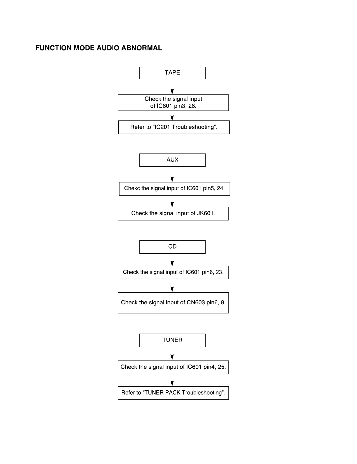
❏ TROUBLESHOOTING
Page 7

- 2-3 -
• OPEN CLOSE NG
Page 8

- 2-4 -
• “ READING ” DISPLAY CHECK
(= ONLY “CD “DISPLAY)
Page 9

- 2-5 -
• READING OK CHECK
(= “NO DISC” DISPLAY)
Page 10

- 2-6 -
• READING OK CHECK #A
(= “NO DISC” DISPLAY)
Page 11

- 2-7 -
• READING OK CHECK #B
(= “NO DISC” DISPLAY)
Page 12

- 2-8 -
• READING OK CHECK #C
(= “NO DISC” DISPLAY)
Page 13

- 2-9 -
• READING OK CHECK #D
(= “NO DISC” DISPLAY)
Page 14

- 2-10 -
• READING OK CHECK #E
(= “NO DISC” DISPLAY)
Page 15

- 2-11 -
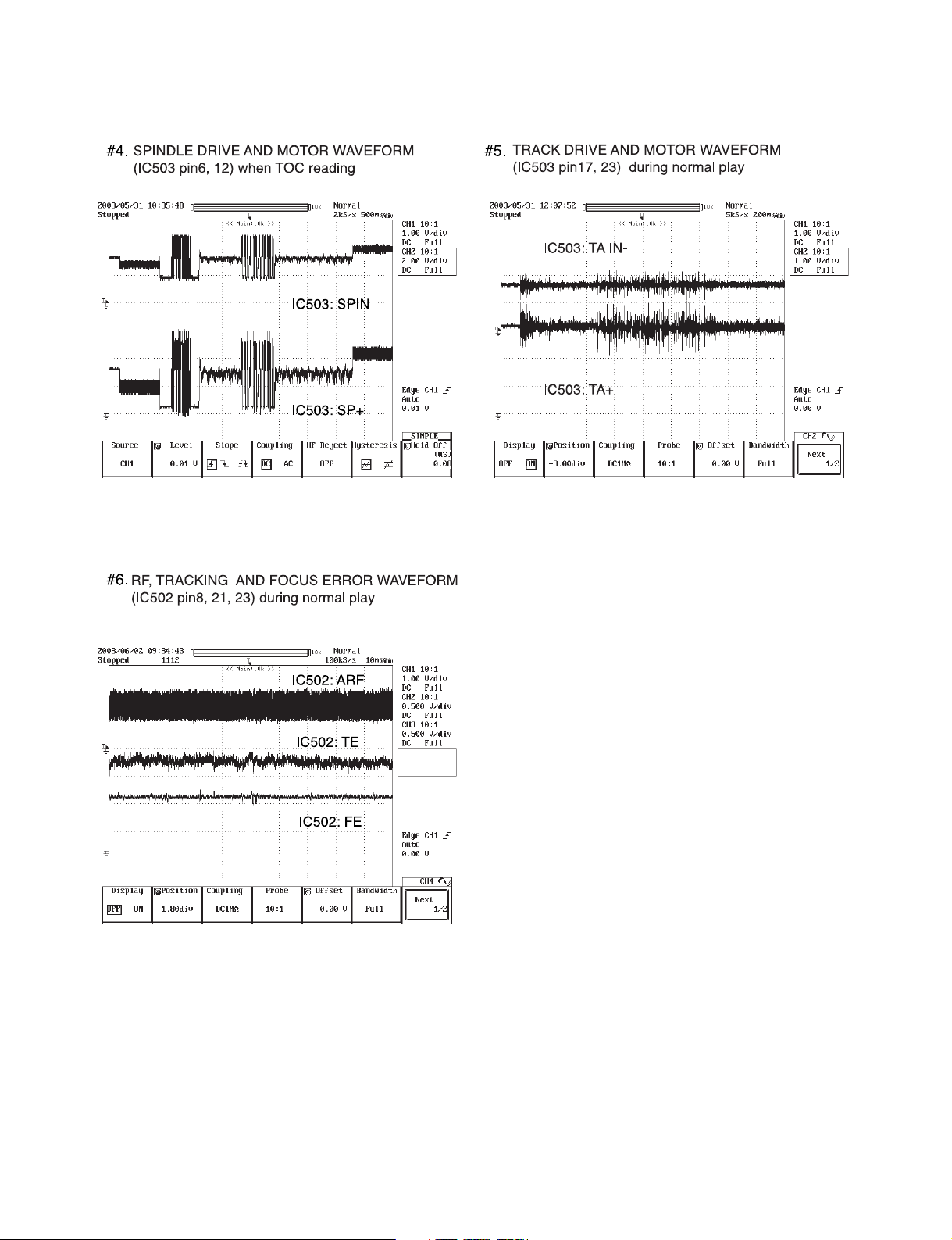
❏ WAVEFORMS OF MAJOR CHECK POINT
TP561
Page 16
- 2-12 -
Page 17

- 2-13 -
❏ AUDIO PART
Page 18

- 2-14 -
Page 19

- 2-15 -
Page 20
- 2-16 -
Page 21

- 2-17 -
Page 22

- 2-18 -
Page 23

- 2-19 -
Page 24

- 2-20 -
MEMO
Page 25

❏ BLOCK DIAGRAM
2-21 2-22
Page 26

2-23 2-24
❏ SCHEMATIC DIAGRAMS
• MAIN SCHEMATIC DIAGRAMS
Page 27
2-25 2-26
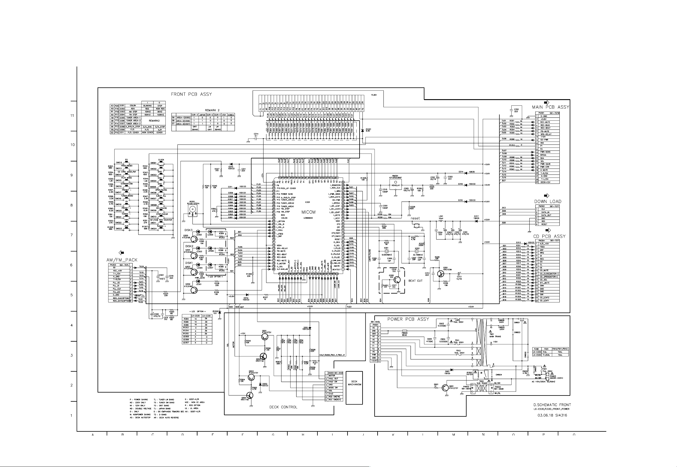
• FRONT/POWER SCHEMATIC DIAGRAM
Page 28

2-27 2-28
• CDP SCHEMATIC DIAGRAM
Page 29

2-29 2-30
❏ WIRING DIAGRAM
Page 30

2-31 2-32
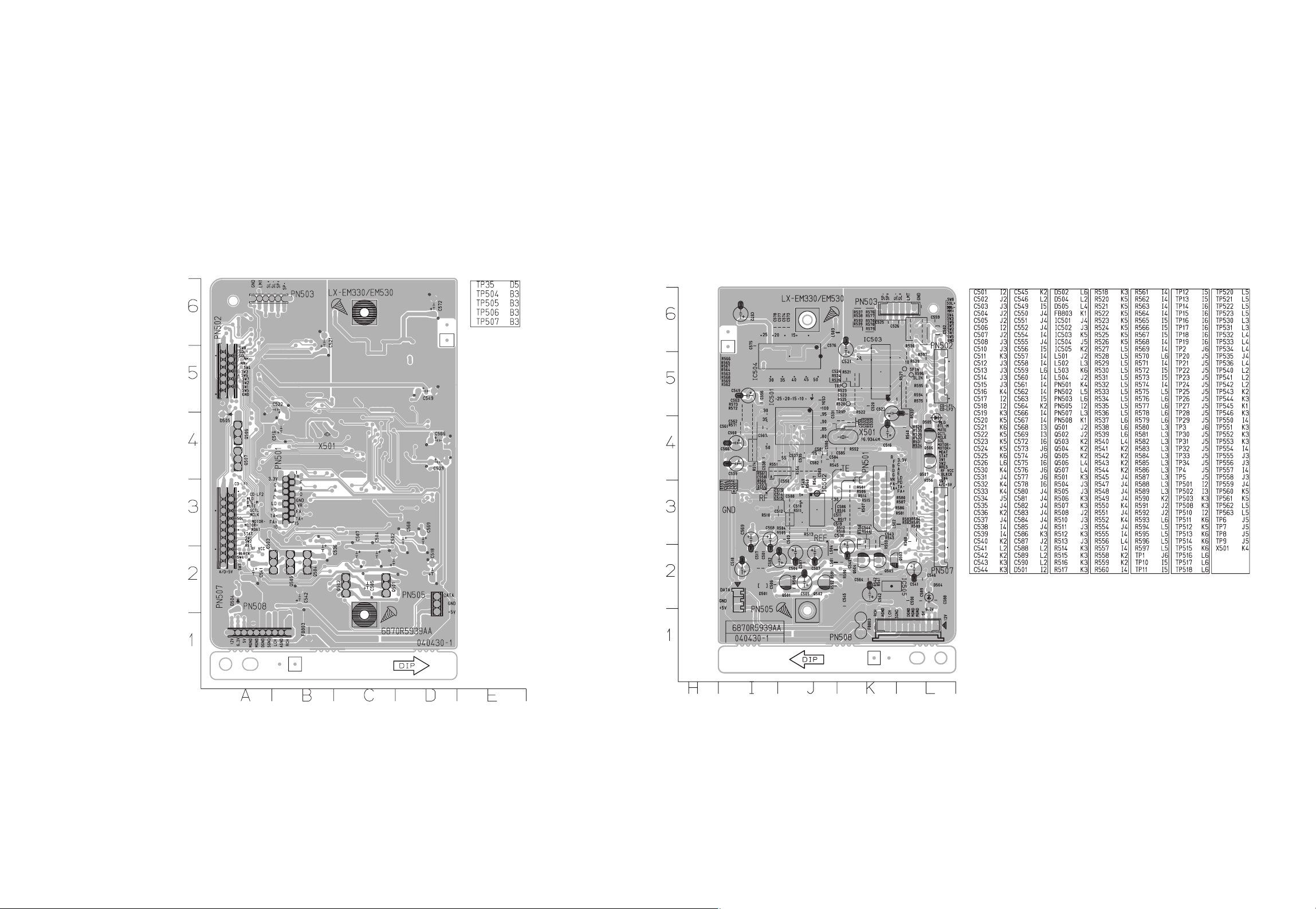
❏ PRINTED CIRCUIT BOARD DIAGRAMS
• MAIN P.C. BOARD(SOLDER SIDE)
Page 31

2-33 2-34
• MAIN P.C. BOARD(COMPONENT SIDE)
Page 32

2-35 2-36
• FRONT/POWER P.C. BOARD (SOLDER SIDE)
Page 33

2-37 2-38
• FRONT/POWER P.C. BOARD (COMPONENT SIDE)
Page 34
2-39 2-40
• CD P.C. BOARD (SOLDER SIDE) • CD P.C. BOARD (COMPONENT SIDE)
Page 35
- 2-41 -
❏ INTERNAL BLOCK DIAGRAM OF ICs
■ KIA6225P/S (IC201)
BIPOLAR LINEAR INTEGRATED CIRCUIT
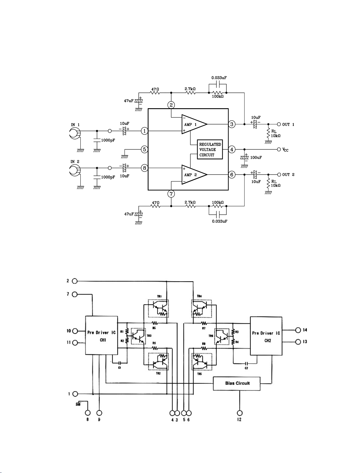
■ STK403-070(IC701)
Equivalent Block Diagram
Page 36

- 2-42 -
■ BA3126N (IC202)
2-channel head switch for radio cassette recoreders
■ BA3308 (IC203)
Dual preamplifier with ALC
• Internal circuit configuration
Page 37
- 2-43 -
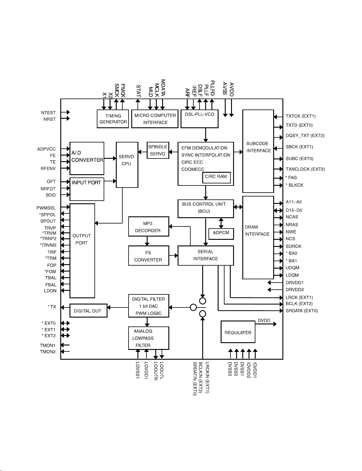
■ IC501 MN6627933
1) PORT ASSIGNMENT
Page 38
- 2-44 -
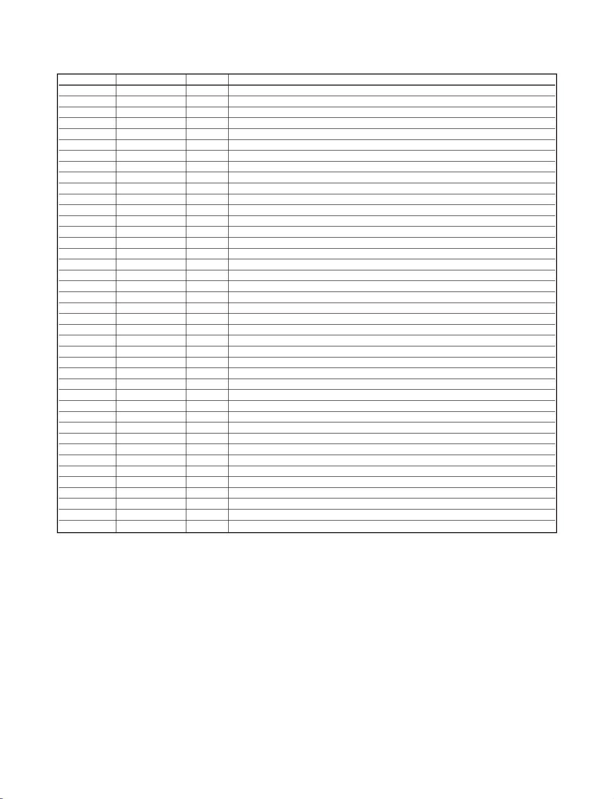
2) Block Diagram
Page 39

- 2-45 -
3) PORT DESCRIPTION
Pin No. Symbol I/O Function
1 D11 I/O DRAM data signal I/O 11
2 D10 I/O DRAM data signal I/O 10
3 D9 I/O DRAM data signal I/O 9
4 D8 I/O DRAM data signal I/O 8
5 UDQM O SDRAM upper byte data mask signal output
6 SDRCK O SDRAM clock signal output
7 A11 O DRAM address signal output 11
8 A9 O DRAM address signal output 9
9 A8 O DRAM address signal output 8
10 A7 O DRAM address signal output 7
11 A6 O DRAM address signal output 6
12 A5 O DRAM address signal output 5
13 A4 O DRAM address signal output 4
14 LDQM O SDRAM lower byte data mask signal output
15 NWE O DRAM write enable signal output
16 NCAS O DRAM CAS control signal output
17 NRAS O DRAM RAS control signal output
18 NCS O SDRAM chip select signal output
19 A3 O DRAM address signal output 3
20 A2 O DRAM address signal output 2
21 A1 O DRAM address signal output 1
22 A0 O DRAM address signal output 0
23 DRVDD1 I Power supply 1 for DRAM interface I/O
24 DVSS1 I Ground 1 for digital circuits
25 A10 O DRAM address signal output 10
26 *BA1 O SDRAM bank selection signal output 1
27 *BA0 O SDRAM bank selection signal output 0
28 DVDD1 I Power supply 1 for internal digital circuits
29 SPOUT O Spindle drive signal output (absolute value)
30 *SPPOL O Spindle drive signal output (polarity)
31 TRVP O Traverse drive signal output (positive polarity)
32 *TRVM O Traverse drive signal output (negative polarity)
33 *TRVP2 O Traverse drive signal output 2 (positive polarity)
34 *TRVM2 O Traverse drive signal output 2 (negative polarity)
35 TRP O Tracking drive signal output (positive polarity)
36 *TRM O Tracking drive signal output (negative polarity)
37 FOP O Focus drive signal output (positive polarity)
38 *FOM O Focus drive signal output (negative polarity)
39 IOVDD1 I Power supply 1 for digital I/O
40 TBAL O Tracking balance adjustment signal output
41 FBAL O Focus balance adjustment signal output
42 FE I Focus error signal input
43 TE I Tracking error signal input
44 ADPVCC I Voltage input for supply voltage monitor
45 RFENV I RF envelope signal input
46 LDON O Laser ON signal output
47 NRFDET I RF detectoion signal input
48 OFT I Off-track signal input
49 BDO I Dropout signal input
50 AVDD1 I Power supply 1 for analog circuits
51 IREF I Analog reference current input
52 ARF I RF signal input
53 DSLF O DSL loop filter pin
54 PWMSEL I PWM output mode selection input Low: Direct High: 3-state
55 PLLF O PLL loop filter pin (for phase comparison)
56 PLLFO O PLL loop filter pin (for speed comparison)
57 AVSS1 I Ground 1 for analog circuits
58 LOOUTL O L-ch audio output for line-out output
59 LOVSS1 I Ground for line-out output
Page 40
- 2-46 -
Pin No. Symbol I/O Function
60 LOOUTR O R-ch audio output for line-out output
61 LOVDD1 I Power supply for line-out output
62 N.C. - 63 TMON1 O Test monitor output 1
64 N.C. - 65 N.C. - 66 TMON2 O Test monitor output 2
67 DVDD3 I Power supply 3 for digital circuits
68 DVSS2 I Ground 2 for digital circuits
69 *EXT0 I/O Expansion I/O port 0
70 *EXT1 I/O Expansion I/O port 1
71 *EXT2 I/O Expansion I/O port 2
72 MCLK I Microcontroller command clock signal input
73 MDATA I Microcontroller command data signal input
74 MLD I Microcontroller command load signal input
75 *STAT O Status signal output
76 *BLKCK O Subcode block clock signal output
77 *SMCK O 4.2336-/8.4672-MHz clock signal output
78 *PMCK O 88.2-kHz clock signal output
79 *TX O Digital audio interface signal output
80 *FLAG O Flag signal output
81 NRST I LSI reset signal input
82 NTEST I Test mode setting input
83 DVSS3 I Ground 3 for digital circuits
84 X1 I Crystal oscillator circuit input
85 X2 O Crystal oscillator circuit output
86 IOVDD2 I Power supply 2 for digital I/O
87 DVDD2 I Power supply 2 for internal digital circuits
88 D2 I/O DRAM data signal I/O 2
89 D1 I/O DRAM data signal I/O 1
90 D0 I/O DRAM data signal I/O 0
91 D3 I/O DRAM data signal I/O 3
92 D4 I/O DRAM data signal I/O 4
93 D5 I/O DRAM data signal I/O 5
94 D6 I/O DRAM data signal I/O 6
95 D7 I/O DRAM data signal I/O 7
96 D15 I/O DRAM data signal I/O 15
97 D14 I/O DRAM data signal I/O 14
98 DRVDD2 I Power supply 2 for DRAM interface I/O
99 D13 I/O DRAM data signal I/O 13
100 D12 I/O DRAM data signal I/O 12
Page 41

- 2-47 -
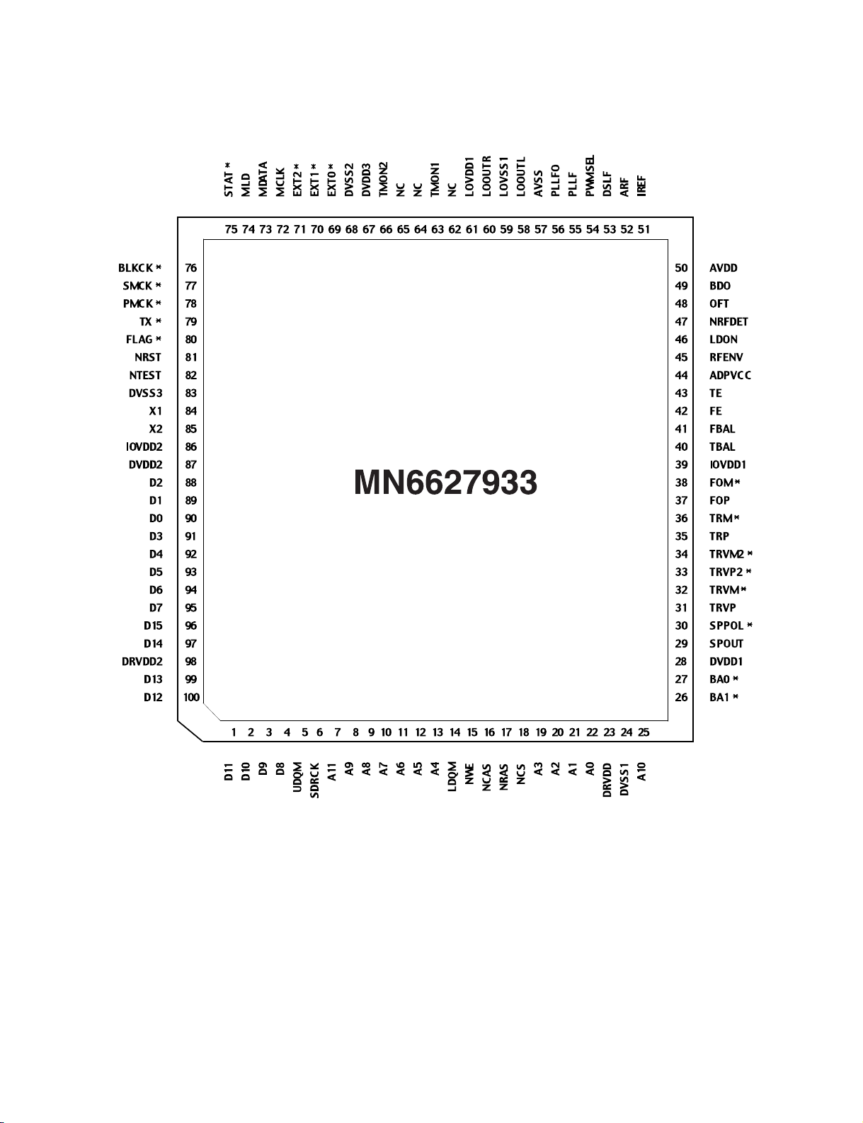
■ IC503 BA5810FP
■ IC504 M12L16161A
1) PORT ASSIGNMENT
28
27
26
25 24
23
22
21 20 19 18 17 16 15
1234 5
6
7891011121314
++— + —
+ —
+ —
+ —
7.5k
7.5k
7.5k
7.5k
LOADING PRE
FWE REV
X3
POWER
SAVE
16k
16k
16k
16k
PREVCC
(PRE. LODING)
PREVCC12
(CH1. CH2)
CD1~
CB4
MUTE
POWVCC34
(CH3, CH4)
10k
10k
10k 10k
10k
10k
10k
10k
LEVEL
SHIFT
LEVEL
SHIFT
LEVEL
SHIFT
LEVEL
SHIFT
10k
10k
10k
10k
10k
10k
Page 42

- 2-48 -
2) BLOCK DIAGRAM
2) PIN Function table
CLK
ADD
LCKE
LRAS
LCBR LWE
CLK
CKE
CS RAS CAS
WE L(U)DQM
LDQM
LWCBR
LCAS
Bank Select
LWE
LDQM
DQI
Data Input Regidter
512K x 16
512K x 16
Column Decoder
Latency & Burst Length
Programming Register
Timing Register
Address Register
Row Decoder
LCBR
LRAS
Sense AMP
I/O Control
Output Buffer
Col. Buffer
Row Buffer
Refresh Counter
Pin Name Input Function
CLK System Clock Active on the positive going edge to sample all inputs.
CS Chip Select Disables or enables device operation by masking or enabling all inputs except
CLK, CKE and L(U)DQM.Masks system clock to freeze operation from the next
clock cycle. CKE
CKE Clock Enable should be enabled at least one cycle prior to new command. Disable input
buffers for power down in standby.
A0~A10/AP
Address Row/Column addresses are multiplexed on the same pins. Row address:
RA0~RA10, column address: CA0~CA7
BA
Bank Select Address
Selects bank to be activated during row address latch time. Selects bank for
read/write during column address latch time.
RAS
Row Address Strobe
Latches row addresses on the positive going edge of the CLK with RAS low.
Enables row access & precharge.
CAS
Column Address Strobe
Latches column addresses on the positive going edge of the CLK with CAS
low. Enables column access.
WE Write Enable Enables write operation and row precharge. Latches data in starting from
CAS, WE active.
L(U)DQM
Data Input / Output Mask
Makes data output Hi-Z, tSHZ after the clock and masks the output. Blocks
data input when L(U)DQM active.
DQ0~15 Data Input / Output Data inputs/outputs are multiplexed on the same pins.
VDD/VSS
Power Supply/Ground
Power and ground for the input buffers and the core logic.
VDDQ/VSSQ Data Output Power/Ground
Isolated power supply and ground for the output buffers to provide improved
noise immunity.
N.C/RFU No Connection/ This is recommended to be left No Connection on the Reserved for Future Use
device.
Page 43

3-1 3-2
• CABINET AND MAIN FRAME SECTION
SECTION 3. EXPLODED VIEWS
351
301
306
305
A47
TUNER
310
311
A46
A43
303
302
A00
284
250
263
286
279
261
260
264
262
280
273
278
272
271
275
274
276
277
285
315
A26
257
A41
NOTE) Refer to “SECTION 5 REPLACEMENT
PARTS LIST” in order to look for the
part number of each part.
Page 44

3-3 3-4
• TAPE DECK MECHANISM: SINGLE AUTO REVERSE DECK
011
003
401
801
007
401
002
506
006
037
016
017
018
019
020
022
A01
015
023
403
504
025
021
505
401
009
507
402
502
401
009
013
406
409
036
035
039
031
029
028
027
040
026
028
038
032
501
502
LOCA.NO. PART NO SPECIFICATION
A00 6720AF0002E CRM4212 TOKYO PIGEON L-SINGLE
A01 6768R-UP03A 50-093-4941 PIGEON PWB ASSY UN
002 6768R-BP03A 02-083-4252 PIGEON BELT/FELT C
003 6768R-PP03A 33-160-4309 PIGEON PRESS CASSE
006 6768R-QP03A 50-093-4891 PIGEON MOTOR(ASSY)
007 6768R-GP03B 50-222-4578 PIGEON GEAR IDLER
008 6768R-SP01F 01-082-4598 PIGEON SPRING CWL4
009 6768R-MP01C 50-219-4014 PIGEON MOLD CWL44
011 6768R-SP01A 01-081-4601 PIGEON SPRING CWL4
013 6768R-SP03A 01-082-4686 PIGEON SPRING CRM4
015 6768R-AP01A 50-268-3016 PIGEON ARM CWL44
016 6768R-GP01H 50-093-4503 PIGEON GEAR CRL442
017 6768R-AP01C 50-239-4072 PIGEON ARM CWL44
018 6768R-GP01J 50-222-4428 PIGEON GEAR CRL442
019 6768R-SP01P 01-081-4678 PIGEON SPRING CRL4
020 6768R-BP01C 02-083-4188 PIGEON BELT/FELT C
021 6768R-LP01C 50-223-4429 PIGEON PULLEY/FLYW
022 6768R-VP03A 50-093-4748 PIGEON SOLENOID AS
023 6768R-GP03A 50-093-4810 PIGEON GEAR ASSY C
025 6768R-JP03B 50-093-31009 PIGEON PULLEY/FLY
026 6768R-SP01D 01-080-4609 PIGEON SPRING CWL4
027 6768R-DP01A 50-259-3342 PIGEON LEVER CWL44
028 6768R-RP01A 22-027-41054 PIGEON ROLLER CWL
029 6768R-MP01A 50-219-4033 PIGEON MOLD CWL44
031 6768R-SP04A 01-082-4731 PIGEON SPRING
032 6768R-EP04A 50-093-41007 PIGEON HEAD ASSY
035 6768R-PP04A 50-119-4915 PIGEON PRESS
036 6768R-SP04B 01-081-4730 PIGEON SPRING
037 6768R-JP03A 50-093-4674 PIGEON PULLEY/FLYW
038 6768R-MP01D 50-219-4034 PIGEON MOLD CWL44
039 6768R-MP02A 50-219-3900 PIGEON MOLD
040 6768R-SP01M 01-080-4607 PIGEON SPRING CWL4
401 6768R-CP01B GSE20A2005 PIGEON SCREW CWL44
402 6768R-CP01A GSE10A2003 PIGEON SCREW CWL44
403 6768R-CP01D GSL10A1704 PIGEON SCREW CWL44
406 6768R-CP01G GSE20A2004 PIGEON SCREW CWL44
409 6768R-CP02A GSD10A2016 PIGEON SCREW
501 6768R-WP03A GWN19S035040 PIGEON WASHER CRM
502 6768R-WP03B 03-000-4532 PIGEON WASHER CRM4
504 6768R-WP01D GWP21X045020 PIGEON WASHER CWL
505 6768R-WP01E GWP12X030040S PIGEON WASHER CW
506 6768R-WP01H GWP23X040020 PIGEON WASHER CWL
507 6768R-WP01F GWN21X040040 PIGEON WASHER CWL
Page 45

3-5 3-6
• TAPE DECK MECHANISM: SINGLE AUTO STOP DECK (OPTIONAL)
401
009
402
003
011
401
009
013
406
407
029
028
401
027
408
030
032
026
023
403
504
025
015
401
008
007
006
016
018
017
019
020
022
A01
021
505
401
002
501
502
Page 46
3-7 3-8
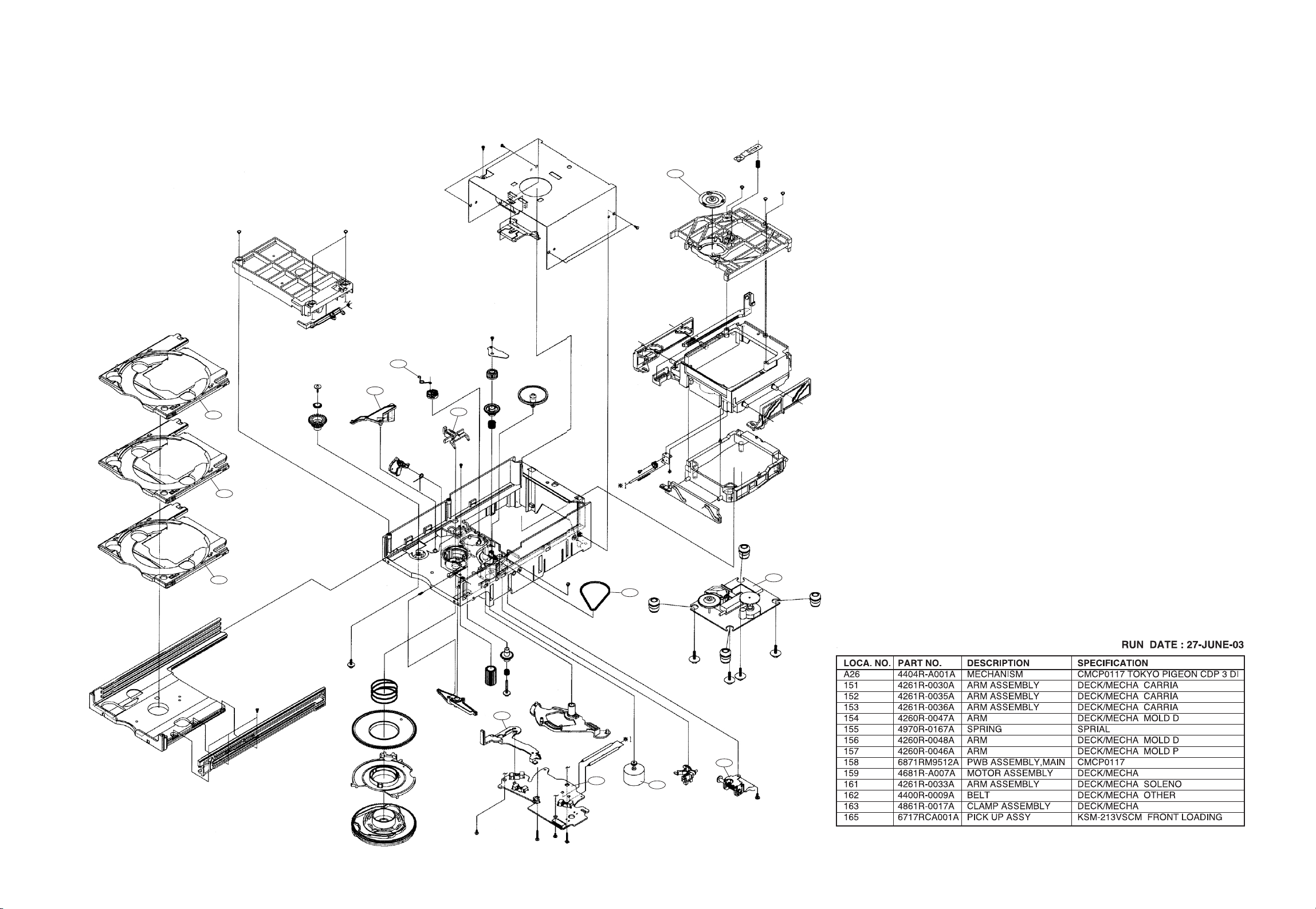
163
155
156
154
162
165
161
159
158
157
153
152
151
❏ CD MECHANISM
Page 47

- 4-1 -
SECTION 4. SPEAKER SECTION
❏ MODEL: LXS-EM530
871
873
868
872
870
869
867
865
863
862
861
850
864
866
LOCA.NO. PART NO DESCRIPTION SPECIFICATION REMARKS
850 3701RM0070F NET ASSEMBLY SPK LXS-EM530 JERSEY NET ASSY
861 3508RMP012B DECORATION LXS-E530 MOLD W/F SILVER SPRAY
862 4930RM0003B HOLDER NET (FE-J220, DECO WF)
863 3720RMM005B PANEL,AUDIO SPK LXS-EM330/EM530 MOLD DARK
864 6400SCSX01D SPEAKER,TWEETER FE-576E SAMMI(DT-13A36L-2)DOME
865 353M025F SCREW,DRAWING TAPTITE, 3X8 FZMY
866 353M050C SCREW,DRAWING BH 3.5X16 FBK
867 6400WSMG03A SPEAKER,WOOFER CW-125B60L-3 SAMMI WOOFER 6OHM
868 4766RM0053A FELT DUCT BLACK LXS-E330/E530
869 4766RM0052A FELT W/F BLACK LXS-E330/E530
870 4766RM0051A FELT T/W BLACK LXS-E330/E530
871 3091RMW075B CABINET ASSEMBLY SPK LXS-EM530 DARK SHEET
872 3610RM0009A FOOT LXS-330, EVA(BLACK) PHI15X1T,
873 6871RU9270C PWB(PCB) ASSEMBLY,SUBSET(AUDIO LXS-E330/E530 2.2UF POSITIVE +
Page 48

- 4-2 -
MEMO
 Loading...