

Page 1

VCR+DVD RECORDER
SERVICE MANUAL
MODEL : LRY-517(RC7793CML)
CAUTION
BEFORE SERVICING THE UNIT, READ THE “SAFETY PRECAUTIONS”
IN THIS MANUAL.
MODEL : LRY-517(RC7793CML)SERVICE MANUAL
P/NO : 3829RGN004H APRIL,2005
Page 2

1-1
SECTION 1
SUMMARY
CONTENTS
PRODUCT SAFETY SERVICING GUIDELINES FOR VIDEO PRODUCTS ............. 1-2
SERVICING PRECAUTIONS .................................................................................................. 1-3
THE STEPS FOR CHANGE THE OPTION CODE ........................................................... 1-4
UP-DATING PROGRAM ........................................................................................................... 1-5
SPECIFICATIONS ...................................................................................................................... 1-7
Page 3
1-2
IMPORTANT SAFETY NOTICE
This manual was prepared for use only by properly trained audio-video service
technicians.
When servicing this product, under no circumstances should the original
design be modified or altered without permission from LG Electronics
Corporation. All components should be replaced only with types identical to
those in the original circuit and their physical location, wiring and lead dress
must conform to original layout upon completion of repairs.
Special components are also used to prevent x-radiation, shock and fire hazard. These components are indicated by the letter “x” included in their component designators and are required to maintain safe performance. No deviations
are allowed without prior approval by LG Electronics Corporation.
Circuit diagrams may occasionally differ from the actual circuit used. This way,
implementation of the latest safety and performance improvement changes
into the set is not delayed until the new service literature is printed.
CAUTION: Do not attempt to modify this product in any way. Never perform
customized installations without manufacturer’s approval. Unauthorized modifications will not only void the warranty, but may lead to property damage or
user injury.
Service work should be performed only after you are thoroughly familiar with
these safety checks and servicing guidelines.
GRAPHIC SYMBOLS
The exclamation point within an equilateral triangle is intended to
alert the service personnel to important safety information in the
service literature.
The lightning flash with arrowhead symbol within an equilateral triangle is intended to alert the service personnel to the presence of
noninsulated “dangerous voltage” that may be of sufficient magnitude to constitute a risk of electric shock.
The pictorial representation of a fuse and its rating within an equilateral triangle is intended to convey to the service personnel the
following fuse replacement caution notice:
CAUTION: FOR CONTINUED PROTECTION AGAINST RISK
OF FIRE, REPLACE ALL FUSES WITH THE SAME TYPE AND
RATING AS MARKED NEAR EACH FUSE.
SERVICE INFORMATION
While servicing, use an isolation transformer for protection from AC line shock.
After the original service problem has been corrected, make a check of the following:
FIRE AND SHOCK HAZARD
1. Be sure that all components are positioned to avoid a possibility of adjacent
component shorts. This is especially important on items trans-ported to and
from the repair shop.
2. Verify that all protective devices such as insulators, barriers, covers, shields,
strain reliefs, power supply cords, and other hardware have been reinstalled
per the original design. Be sure that the safety purpose of the polarized line
plug has not been defeated.
3. Soldering must be inspected to discover possible cold solder joints, solder
splashes, or sharp solder points. Be certain to remove all loose foreign particles.
4. Check for physical evidence of damage or deterioration to parts and components, for frayed leads or damaged insulation (including the AC cord), and
replace if necessary.
5. No lead or component should touch a high current device or a resistor rated
at 1 watt or more. Lead tension around protruding metal surfaces must be
avoided.
6. After reassembly of the set, always perform an AC leakage test on all
exposed metallic parts of the cabinet (the channel selector knobs, antenna
terminals, handle and screws) to be sure that set is safe to operate without
danger of electrical shock. DO NOT USE A LINE ISOLATION TRANSFORMER DURING THIS TEST. Use an AC voltmeter having 5000 ohms per
volt or more sensitivity in the following manner: Connect a 1500 ohm, 10
watt resistor, paralleled by a .15 mfd 150V AC type capacitor between a
known good earth ground water pipe, conduit, etc.) and the exposed metallic parts, one at a time. Measure the AC voltage across the combination of
1500 ohm resistor and .15 mfd capacitor. Reverse the AC plug by using a
non-polarized adaptor and repeat AC voltage measurements for each
exposed metallic part. Voltage measured must not exceed 0.75 volts RMS.
This corresponds to 0.5 milliamp AC. Any value exceeding this limit constitutes a potential shock hazard and must be corrected immediately.
TIPS ON PROPER INSTALLATION
1. Never install any receiver in a closed-in recess, cubbyhole, or closely fitting
shelf space over, or close to, a heat duct, or in the path of heated air flow.
2. Avoid conditions of high humidity such as: outdoor patio installations where
dew is a factor, near steam radiators where steam leakage is a factor, etc.
3. Avoid placement where draperies may obstruct venting. The customer
should also avoid the use of decorative scarves or other coverings that
might obstruct ventilation.
4. Wall- and shelf-mounted installations using a commercial mounting kit must
follow the factory-approved mounting instructions. A product mounted to a
shelf or platform must retain its original feet (or the equivalent thickness in
spacers) to provide adequate air flow across the bottom. Bolts or screws
used for fasteners must not touch any parts or wiring. Perform leakage tests
on customized installations.
5. Caution customers against mounting a product on a sloping shelf or in a tilted position, unless the receiver is properly secured.
6. A product on a roll-about cart should be stable in its mounting to the cart.
Caution the customer on the hazards of trying to roll a cart with small casters across thresholds or deep pile carpets.
7. Caution customers against using extension cords. Explain that a forest of
extensions, sprouting from a single outlet, can lead to disastrous consequences to home and family.
PRODUCT SAFETY SERVICING GUIDELINES FOR VIDEO PRODUCTS
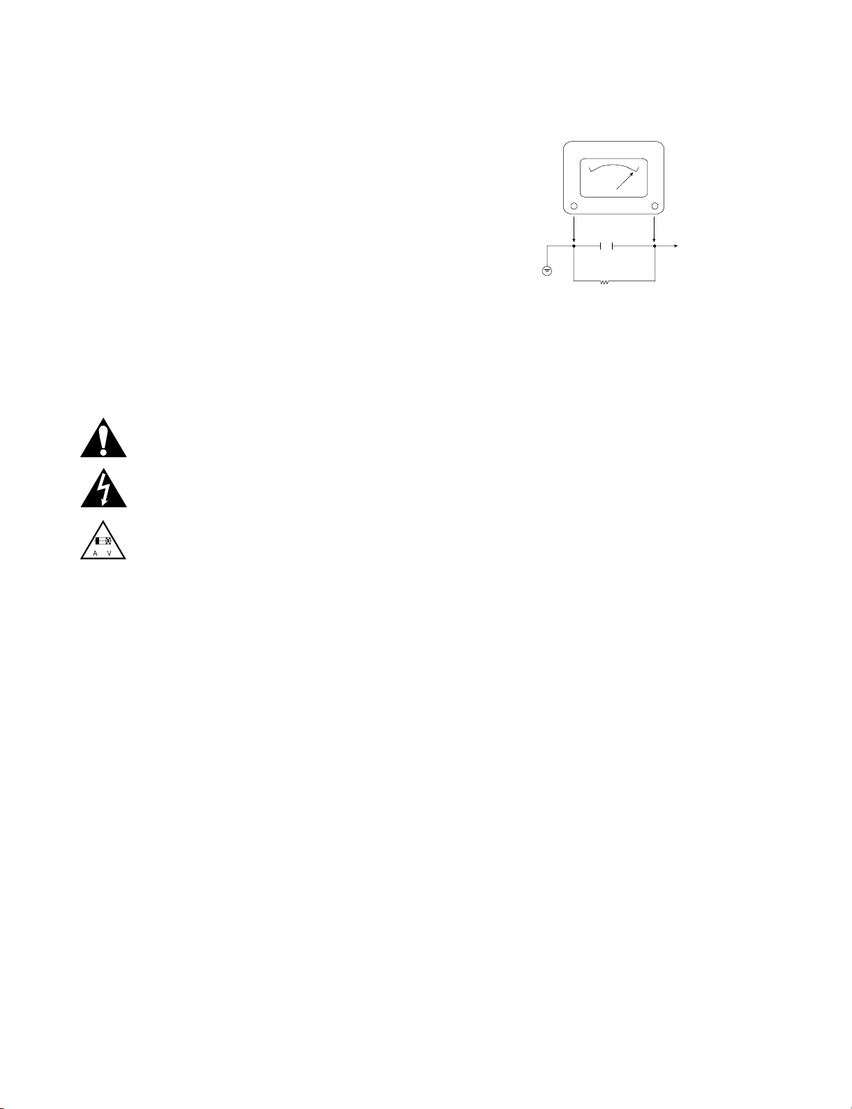
A.C. Voltmeter
Good Earth Ground
such as the Water
Pipe, Conduit, etc.
0.15uF
1500 OHM
10 WATT
Place this probe
on each exposed
metal part.
Page 4

1-3
SERVICING PRECAUTIONS
CAUTION: Before servicing the VCR + DVD RECODER covered by this service data and its supplements and addends,
read and follow the
SAFETY PRECAUTIONS. NOTE: if
unforeseen circumstances create conflict between the following servicing precautions and any of the safety precautions in this publications, always follow the safety precautions.
Remember Safety First:
General Servicing Precautions
1. Always unplug the VCR + DVD RECODER AC power cord
from the AC power source before:
(1) Removing or reinstalling any component, circuit board,
module, or any other assembly.
(2) Disconnecting or reconnecting any internal electrical
plug or other electrical connection.
(3) Connecting a test substitute in parallel with an elec-
trolytic capacitor.
Caution: A wrong part substitution or incorrect
polarity installation of electrolytic capacitors may result
in an explosion hazard.
2. Do not spray chemicals on or near this VCR + DVD
RECODER or any of its assemblies.
3. Unless specified otherwise in this service data, clean
electrical contacts by applying an appropriate contact
cleaning solution to the contacts with a pipe cleaner,
cotton-tipped swab, or comparable soft applicator.
Unless specified otherwise in this service data, lubrication
of contacts is not required.
4. Do not defeat any plug/socket B+ voltage interlocks with
whitch instruments covered by this service manual might
be equipped.
5. Do not apply AC power to this VCR + DVD RECODER
and / or any of its electrical assemblies unless all solidstate device heat sinks are correctly installed.
6. Always connect the test instrument ground lead to an
appropriate ground before connecting the test instrument
positive lead. Always remove the test instrument ground
lead last.
Insulation Checking Procedure
Disconnect the attachment plug from the AC outlet and turn
the power on. Connect an insulation resistance meter (500V)
to the blades of the attachment plug. The insulation resistance between each blade of the attachment plug and accessible conductive parts (Note 1) should be more than 1Mohm.
Note 1: Accessible Conductive Parts include Metal panels,
Input terminals, Earphone jacks,etc.
Electrostatically Sensitive (ES) Devices
Some semiconductor (solid state) devices can be damaged
easily by static electricity. Such components commonly are
called Electrostatically Sensitive (ES) Devices. Examples of
typical ES devices are integrated circuits and some field
effect transistors and semiconductor chip components.
The following techniques should be used to help reduce the
incidence of component damage caused by static electricity.
1. Immediately before handling any semiconductor component or semiconductor-equipped assembly, drain off any
electrostatic charge on your body by touching a known
earth ground. Alternatively, obtain and wear a commercially available discharging wrist strap device, which
should be removed for potential shock reasons prior to
applying power to the unit under test.
2. After removing an electrical assembly equipped with ES
devices, place the assembly on a conductive surface such
as aluminum foil, to prevent electrostatic charge buildup or
exposure of the assembly.
3. Use only a grounded-tip soldering iron to solder or unsolder
ES devices.
4. Use only an anti-static solder removal device. Some
solder removal devices not classified as “anti-static” can
generate electrical charges sufficient to damage ES
devices.
5. Do not use freon-propelled chemicals. These can
generate an electrical charge sufficient to damage ES
devices.
6. Do not remove a replacement ES device from its protective package until immediately before you are ready to
install it. (Most replacement ES devices are packaged with
leads electrically shorted together by conductive foam,
aluminum foil,or comparable conductive material).
7. Immediately before removing the protective material from
the leads of a replacement ES device, touch the protective
material to the chassis or circuit assembly into which the
device will be installed.
Caution: Be sure no power is applied to the chassis or
circuit, and observe all other safety precautions.
8. Minimize bodily motions when handling unpackaged
replacement ES devices. (Normally harmless motion such
as the brushing together of your clothes fabric or the lifting
of your foot from a carpeted floor can generate static electricity sufficient to damage an ES device.)
Page 5
1-4
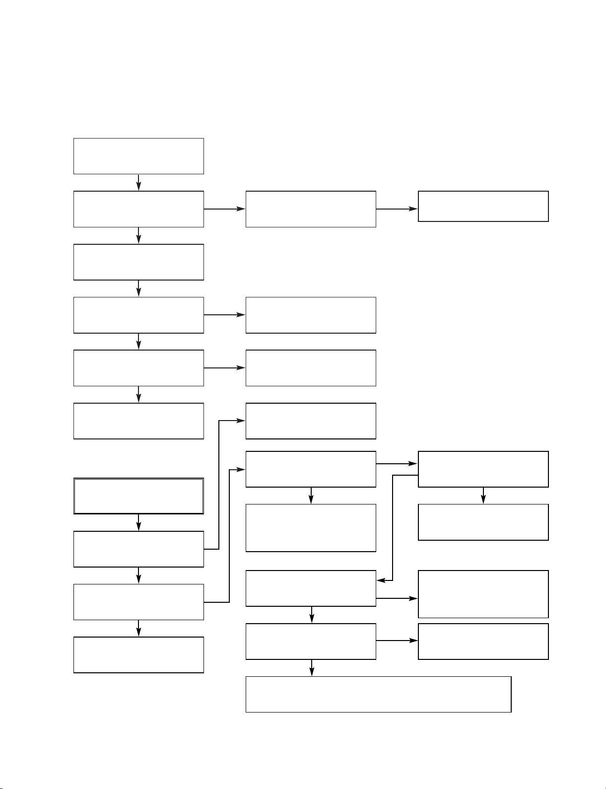
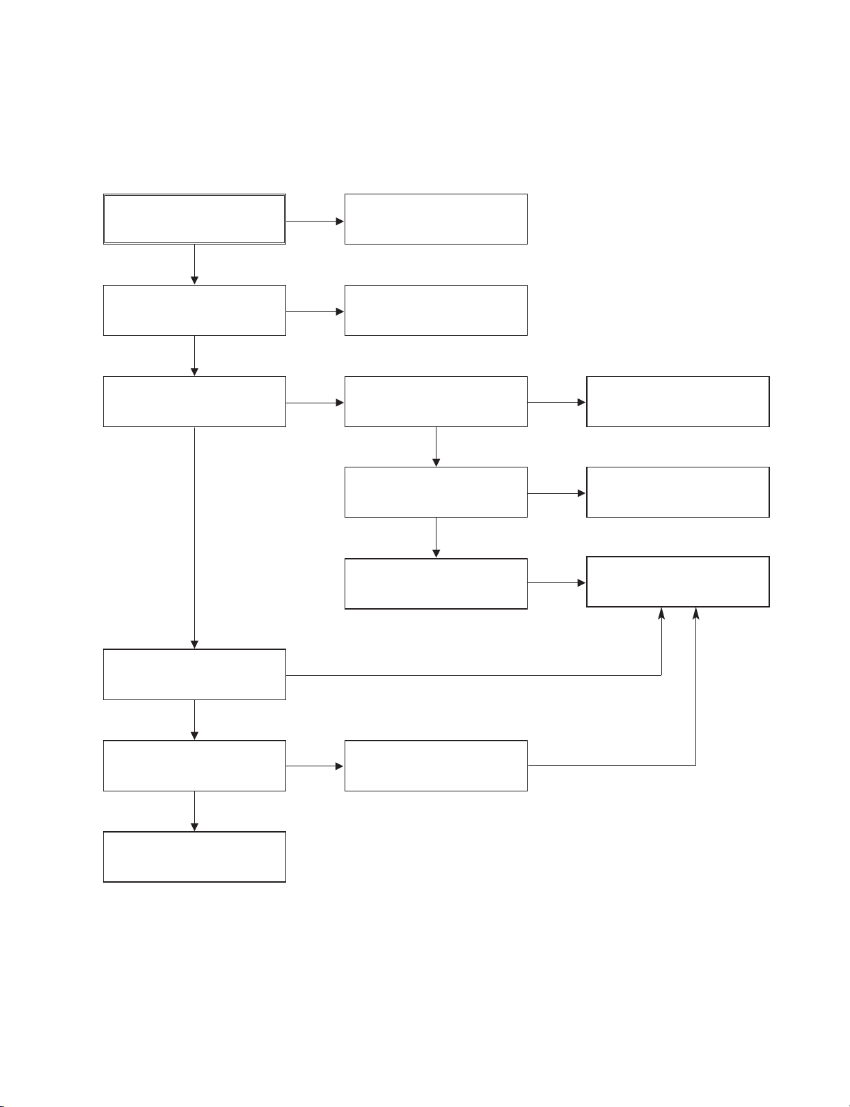
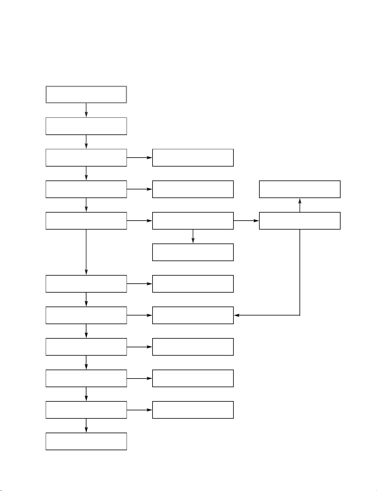
THE STEPS FOR CHANGE THE OPTION CODE
Push Switch POWER ON/ OFF
at remocon or timer keyborad
Select DVD MODE at the set
use remocon or timer keyborad
Push REC+ PLAY
at timer keyboard
Use remocon and push ENTER
Use Direction Key at
remocon (LEFT/ RIGHT)
for select the position of option
Use Direction Key
at remocon (UP/ DOWN)
for change the option
After finish edit code of option
push ENTER at remocon
For finishing and intialized
the option code push
REC + EJECT at remocon
Note : This procedure must be done when IC304(On digital Board) or Digital Boardassy
LRY-517
NAME HEX
OPT1 F2
OPT255
OPT353
OPT4 FD
OPT5 17
OPT6 0C
OPT7 21
OPT8 00
Press “Enter” key
to Save and Exit
DETECT NEW EEPROM (OPTION EDIT SCREEN)
Page 6
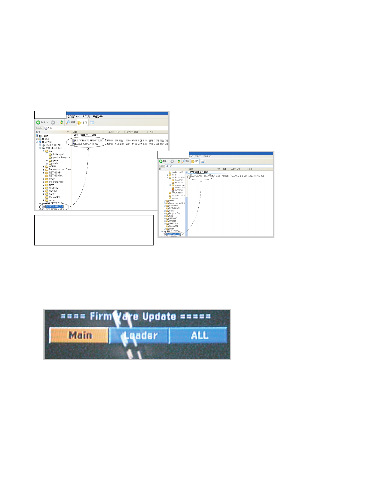
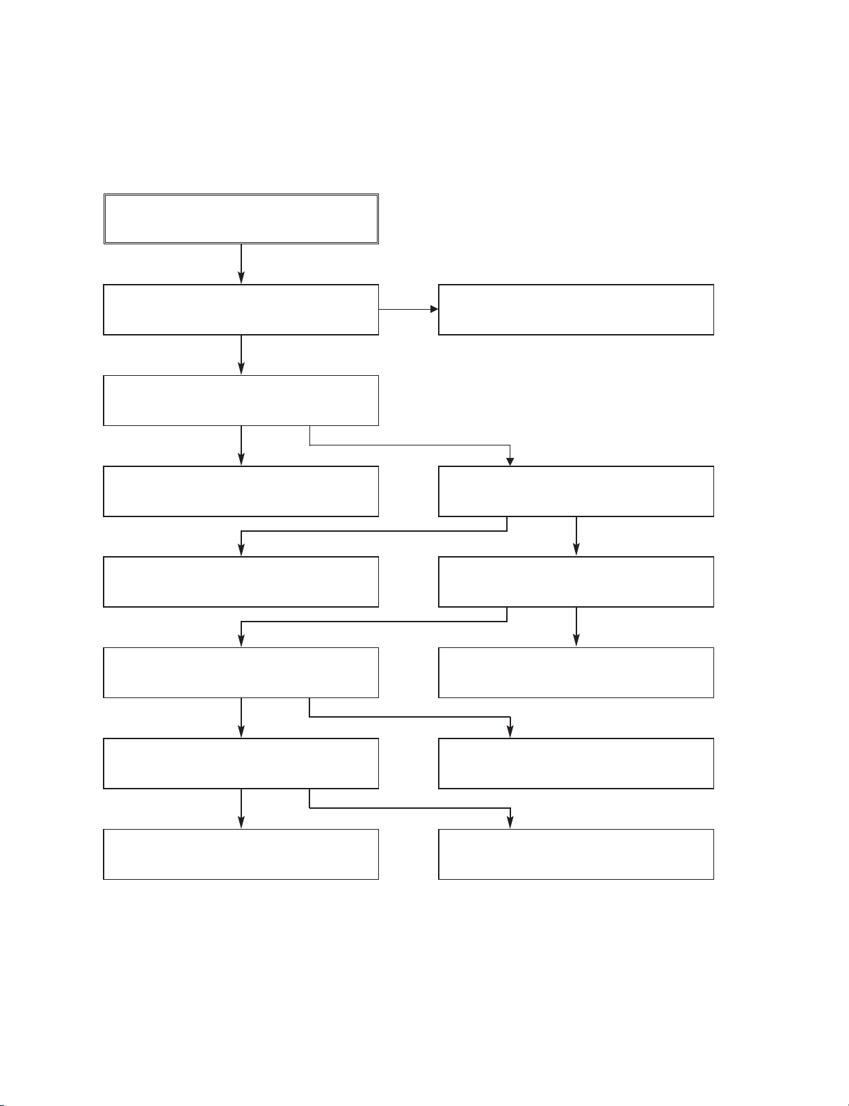
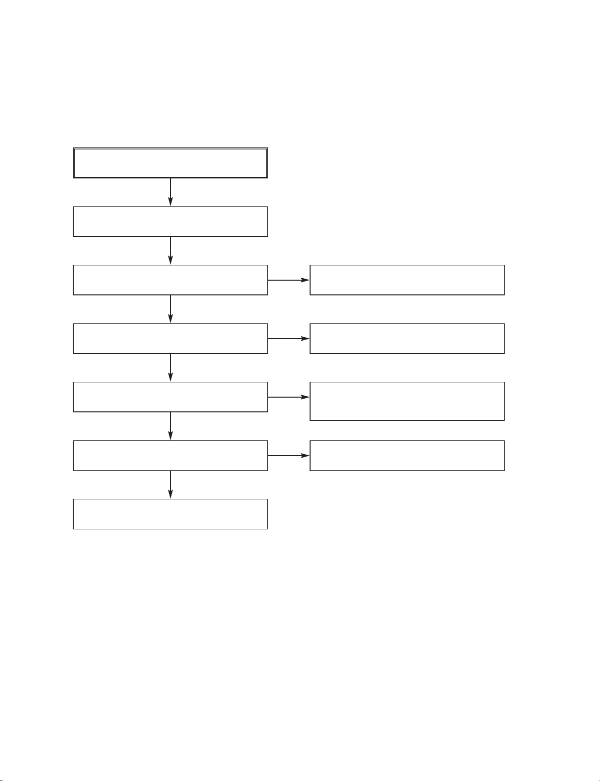
BURNING DISC
• For up-dating the DVD program using the disc, it must burning the disc which include the DVD software.
• For recorder combi set which using the disc downloader program are DVD Program and Loader Program.
• In 2nd generation for recorder combi can download the DVD program and Loader program one by one, or all
together.
• If you format like number 1 you’ll see capture like (figure 1)
• And you have three choice:
1. Main. It’s mean if you chose this it’ll up-dating only DVD prgram.
2. Loader.It’s mean if you chose this it’ll up-dating only Loader program.
3. ALL. It’s mean if you chose this it’ll up-dating DVD and Loader program.
• If you format like number 2 you’ll not see capture like figure 1 that give you choices, you have no choice only
update DVD program
1-5
UP-DATING PROGRAM
* There is two way to format disc DVD Program
1. DVD and LOADER program format in one
disc
2. Only DVD program format in one disc
(Figure 1)
Number 1
Number 2
Page 7
1-6
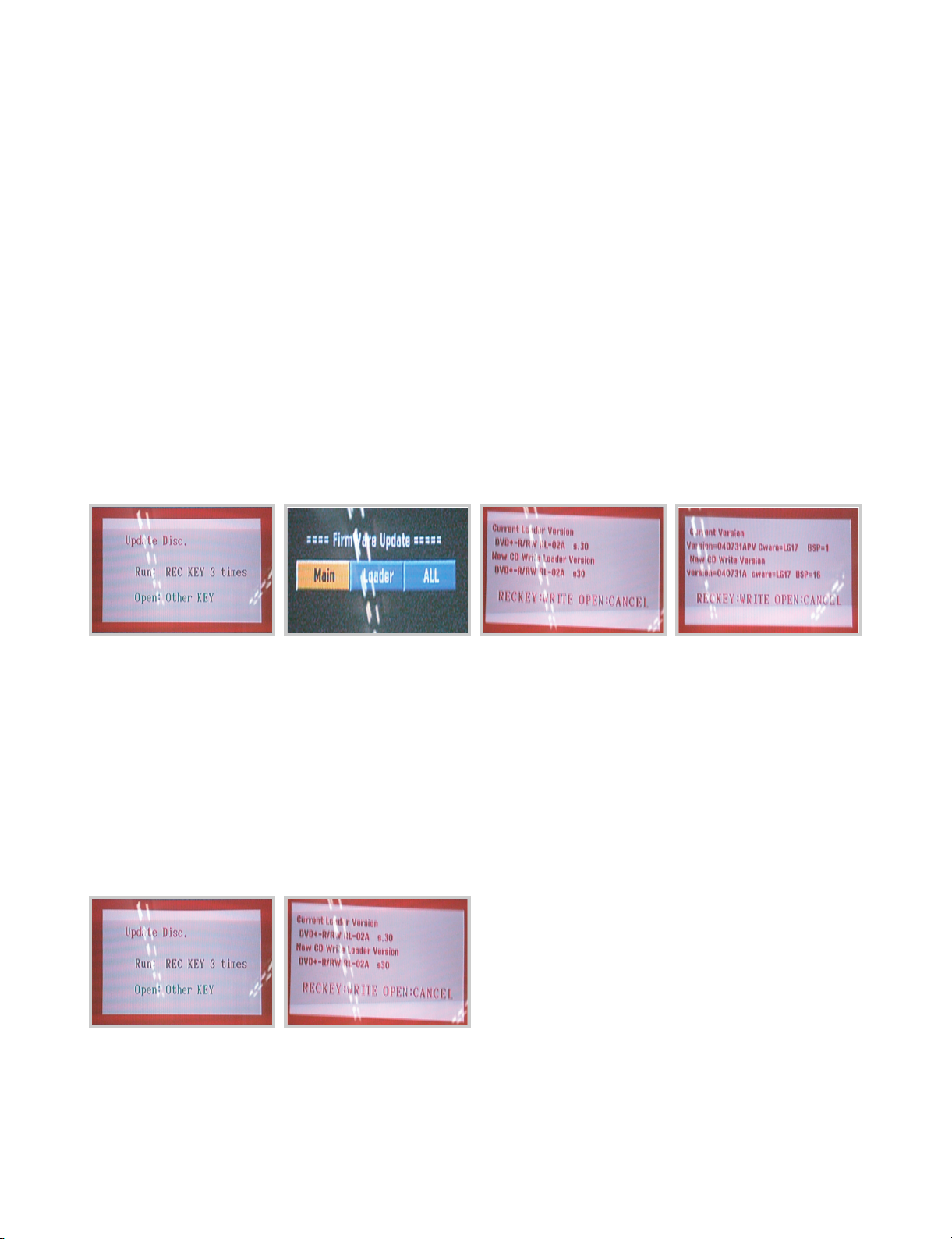
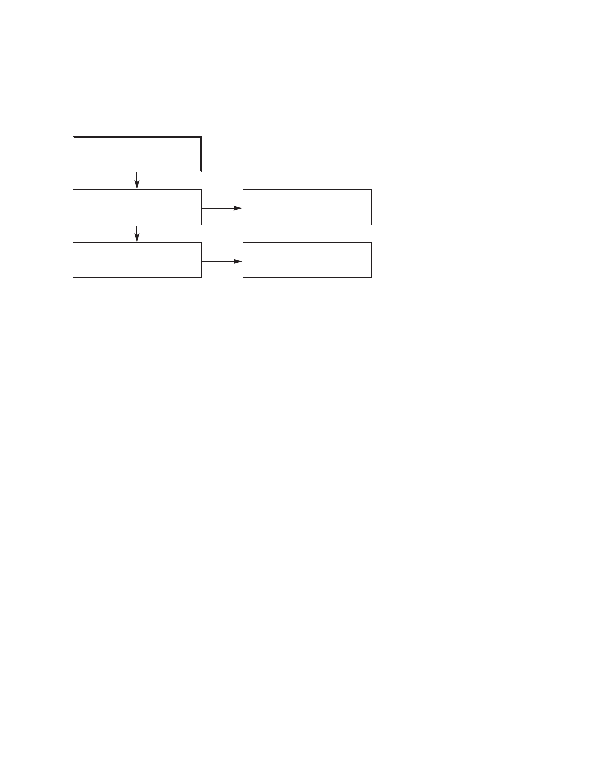
DVD UPGRADE INSTRUCTION
FORMAT NO 1
1. Press POWER KEY to turn on.
2. After booting, insert the upgrade disc, and you will see massage like [FIGURE 1]
3. Press “REC” key (front or remote) 3 times and you will see as [FIGURE 2] with remote Chose one of them
then Press enter
4. For update both of them [MAIN & LOADER] we chose “ALL” and first you will see [FIGURE 3] DVD update
→ Check the “Current Version” and “ New CD Write Version” and press “REC” key.
5. The DVD update will be on progress.And when finish update MAIN Version it’s automatically continue to
Update Loader Version and You will see [FIGURE 4]
→ Check the “Current Version” and “New CD Write Version “ and Press “REC” key once more
6. The LOADER update will be on progress. And tray will open.
7. Remove the disc and wait until finish
8. The tray will be close and open automatically after completing “UNDER UPDATE” 100%
9. Turn off the unit
10. Turn on again the unit is operation with new software
FORMAT NO 2
1. Press POWER KEY to turn on.
2. After booting, insert the upgrade disc, and you will see massage like [FIGURE 1]
3. Press “REC” key (front or remote) 3 times
4. The DVD update will be on progress.
→ Check the “Current Version” and “New CD Write Version “ and Press “REC” key once more
5. The tray will be open automatically after completing “UNDER UPDATE” 100%
6. Remove the disc andTurn off the unit
7. Turn on again the unit is operation with new software
[FIGURE 1] [FIGURE 2] [FIGURE 3] [FIGURE 4]
[FIGURE 1] [FIGURE 2]
Page 8

1-7
SPECIFICATIONS
General
Power requirements AC 120V, 60 Hz
Power consumption 35W
Dimensions (approx.) 430 X 78.5 X 354 mm (w x h x d)
Mass (approx.) 5.7 kg
Operating temperature 5°C to 35°C
Operating humidity 5 % to 90 %
Television system NTSC color system
Recording format NTSC
System
Laser Semiconductor laser, wavelength 650 mm
Video head system Double azimuth 4 heads, helical scanning
Signal system NTSC
Recording
Recording format DVD+RW/+R Video format
Recordable discs DVD-ReWritable, DVD-Recordable, DVD+ReWritable, DVD+Recordable
Recordable time Approx. 1 hour (XP mode), 2 hours (SP mode), 4 hours (LP mode),
6 hours (EP mode)
Video recording format
Sampling frequency 27MHz
Compression format MPEG 2
Audio recording format
Sampling frequency 48kHz
Compression format Dolby Digital
Playback
Frequency response DVD (PCM 48 kHz): 8 Hz to 22 kHz, CD: 8 Hz to 20 kHz
DVD (PCM 96 kHz): 8 Hz to 44 kHz
Harmonic distortion Less than 0.008% (AUDIO OUT connector)
Dynamic range More than 95 dB (AUDIO OUT connector)
Inputs
RF IN RF input, 75 ohms
VIDEO IN 1.0 Vp-p 75 ohms, sync negative, RCA jack
AUDIO IN 0 dBm more than 47 kohms, RCA jack (L, R)
DV IN 4 pin (i.LINK/IEEE 1394 standard)
S-VIDEO IN (Y) 1.0 V (p-p), 75 Ω, negative sync, Mini DIN 4-pin x 1
(C) 0.3 V (p-p) 75 Ω
Outputs
S-VIDEO OUT (Y) 1.0 V (p-p), 75 Ω, negative sync, Mini DIN 4-pin x 1
(C) 0.3 V (p-p) 75 Ω
COMPONENT VIDEO OUT (Y) 1.0 V (p-p), 75 Ω, negative sync, RCA jack x 1
(Pb)/(Pr) 0.7 V (p-p), 75 Ω, RCA jack x 2
Audio output (digital audio) 0.5 V (p-p), 75 Ω, RCA jack x 1
Audio output (analog audio) 2.0 Vrms (1 KHz, 0 dB), 600 Ω, RCAjack (L, R) x 1
* Design and specifications are subject to change without notice.
* Manufactured under license from Dolby Laboratories. “Dolby”, “Pro Logic” and the double-D symbol are trademarks of
Dolby Laboratories.
* DTS and DTS Digital Out are registered trademarks of Digital Theater Systems, Inc.
Page 9

2-1
SECTION 2
EXPLODED VIEWS
CONTENTS
EXPLODED VIEWS .....................................................................................................................2-2
1. Cabinet and Main Frame Section ...........................................................................................2-2
2. Packing Accessory Section ....................................................................................................2-4
Page 10
2-2
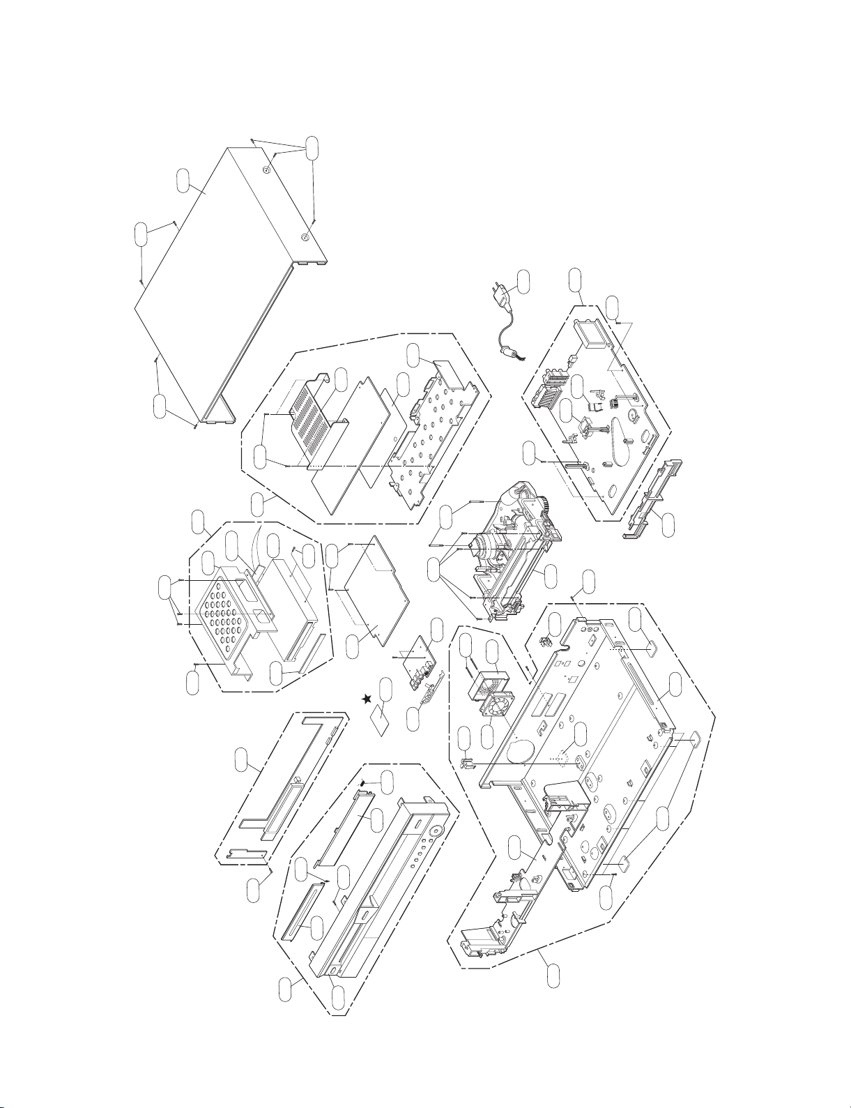
EXPLODED VIEWS
1. Cabinet and Main Frame Section
463
250
463
463
A00
265
A46
469
321
323
276
465
261
320
300
257
255
469
A47
A60
A26
A26A
290
7
45
7
45
291
459
469
A52
A54
256
457
A48
470
468
469
263
A50
457
A43
274
264
266
284
283
260
286
469
285
280
261
261
452
A44
Page 11
2-3
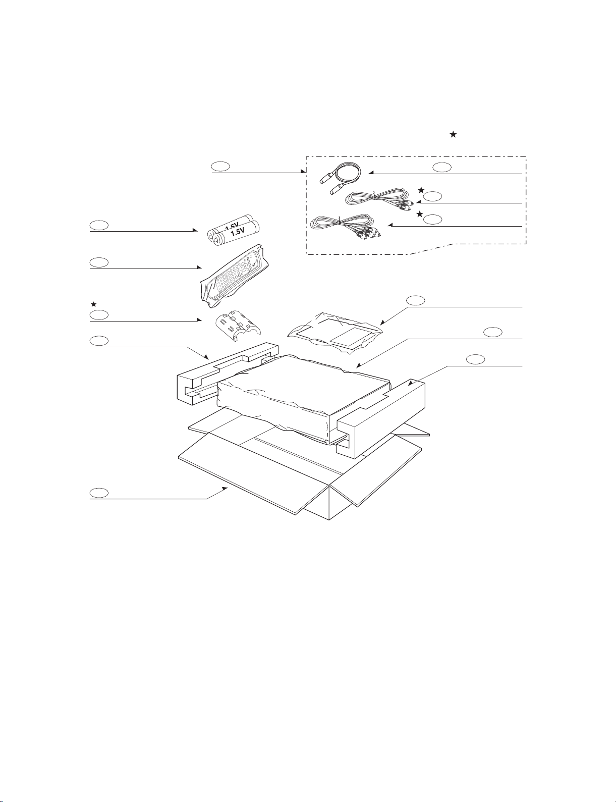
2. Packing Accessory Section
810
808
BATTERY
900
REMOCON
826
FILTER
803
P
ACKING
CABLE ASS'Y
RF
OPTIONAL PARTS
806
CABLE(COAXIAL)
811
PLUG ASS'Y 1WAY
812
PLUG ASS'Y 2WAY
INSTRUCTION ASSEMBLY
801
803
804
P
ACKING
BAG
802
BOX CARTO
N
Page 12

3-1
SECTION 3
ELECTRICAL
CONTENTS
OVERALL WIRING DIAGRAM..............................3-2
VCR PART
ELECTRICAL ADJUSTMENT
PROCEDURES
............................................................3-3
VCR ELECTRICAL TROUBLESHOOTING
GUIDE
.............................................................................3-4
1. POWER(SMPS) CIRCUIT .......................................3-4
2. SYSTEM/KEY CIRCUIT ..........................................3-7
3. SERVO CIRCUIT.....................................................3-8
4. Y/C CIRCUIT..........................................................3-11
5. HI-FI CIRCUIT .......................................................3-15
6. TUNER/IF CIRCUIT...............................................3-18
BLOCK DIAGRAMS................................................3-20
1. POWER(SMPS) BLOCK DIAGRAM......................3-20
2. AVCP BLOCK DIAGRAM ......................................3-22
3. SYSTEM BLOCK DIAGRAM.................................3-24
4. JACK BLOCK DIAGRAM ......................................3-26
5. STUNER/MTZ BLOCK DIAGRAM.........................3-28
6. AVCP BLOCK DIAGRAM ......................................3-30
CIRCUIT DIAGRAMS..............................................3-32
1. POWER(SMPS) CIRCUIT DIAGRAM ...................3-32
2. TU/IF CIRCUIT DIAGRAM ....................................3-34
3. A/V CIRCUIT DIAGRAM........................................3-36
4. HI-FI CIRCUIT DIAGRAM .....................................3-38
5. SYSTEM CIRCUIT DIAGRAM...............................3-40
6. JACK CIRCUIT DIAGRAM
(SCART MODEL ONLY) ........................................3-42
7. TIMER CIRCUIT DIAGRAM ..................................3-44
• WAVEFORMS .........................................................3-46
• CIRCUIT VOLTAGE CHART ...................................3-48
PRINTED CIRCUIT DIAGRAMS .........................3-50
1. VCR P.C.BOARD...................................................3-50
2. SMPS P.C.BOARD ...............................................3-52
3. JACK P.C.BOARD ................................................3-54
4. HDD P.C.BOARD...................................................3-55
5. KEY P.C.BOARD .................................................3-56
6. TIMER P.C.BOARD .............................................3-56
VDR PART
VDR ELECTRICAL TROUBLESHOOTING
GUIDE
...........................................................................3-58
1. POWER(SMPS) CIRCUIT .....................................3-58
2. NO COMPONENT VIDEO SIGNAL WHEN
PLAYING DISC......................................................3-60
3. NO COMPOSITE / S-VIDEO SIGNAL WHEN
PLAYING DISC......................................................3-61
4. NO TV, EXTERNAL INPUT VIDEO SIGNAL.........3-62
5. WHEN PLAYING DISC, NO AUDIO OUTPUT ......3-63
6. NO TUNER AUDIO OUTPUT ................................3-63
7. NO OPTICAL / DIGITAL OUTPUT ........................3-63
8. NO EXTERNAL INPUT 1, 2 AUDIO......................3-64
9. NO EXTERNAL INPUT 3 AUDIO ..........................3-64
BLOCK DIAGRAMS................................................3-65
1. VDR SET TOTAL BLOCK DIAGRAM....................3-65
2. VDR MAIN H/ W BLOCK DIAGRAM .....................3-66
3. POWER BLOCK DIAGRAM..................................3-67
4. AUDIO IN/ OUT BLOCK DIAGRAM ......................3-68
5. CPU & CONTROL REGISTER
BLOCK DIAGRAM.................................................3-69
6. VIDEO IN/ OUT BLOCK DIAGRAM ......................3-70
7. DV 1394 IN/OUT BLOCK DIAGRAM ....................3-71
8. MEMORY CARD IN/ OUT BLOCK DIAGRAM ......3-72
CIRCUIT DIAGRAMS..............................................3-73
1. BGA 308P CIRCUIT DIAGRAM.............................3-73
2. DDR & B TO B CONNECTOR
CIRCUIT DIAGRAM ..............................................3-75
3. POWER, FLASH, CONNECTOR CIRCUIT
DIAGRAM ..............................................................3-77
4. RST, CONTROL/STATUS_REG., ATAPI,
HOST_CPLD, LATCH CIRCUIT DIAGRAM ..........3-79
5. VIDEO_IN, VIDEO_OUT CIRCUIT DIAGRAM......3-81
6. DV1394, HDMI CIRCUIT DIAGRAM .....................3-83
7. AUDIO IN/OUT CIRCUIT DIAGRAM .....................3-85
• WAVEFORMS .........................................................3-87
• CIRCUIT VOLTAGE CHART ...................................3-89
PRINTED CIRCUIT DIAGRAMS .........................3-91
1. VDR P.C.BOARD(TOP VIEW) ...............................3-91
2. VDR P.C.BOARD(BOTTOM VIEW) .......................3-93
Page 13
3-2
1514131211
10
987654321
1
2
3
4
5
6
7
8
9
10
11
12
13
14
15
16
17
18
19
20
21
1
2
3
4
5
6
7
8
9
10
11
12
13
14
15
16
17
18
19
20
21
SPD.F
GND
INTR/PROG
NC
GND
RADIO'H'
AMP ON
VDR REDET
NC
NC
NC
VDR CLK
DATA(VCR-VDR)
DATA(VDR-VCR)
VDR ENA
AMP CLK
AMP RX
AMP TX
AMP READY
AMP MUTE
NC
1514131211
10
987654321
P6603
P6602
PM601PN302
PN302
PN301
PN301
PMD01PMD02
PN304
CON401
CON401
PPM01
P101
P3D01P3D03
P104
P103
P103
P104
P3D02
P3D02
PMC01
PMC01
P3D03
P3D01
PN303
PM602
PM603 P6M01
13.5VA(DRUM)
A/E(-)
A/E(+)
CFG
CAP.VCC
SERVO VCC
CAP.REV'H'
I-LIMIT
MOTOR GND
S.GND
DRUM VCC(13.5VA)
CAP.CTL
L/M CTL
DPG/DFG
DRUM CTL
8.7V
GND12
1
2
R493
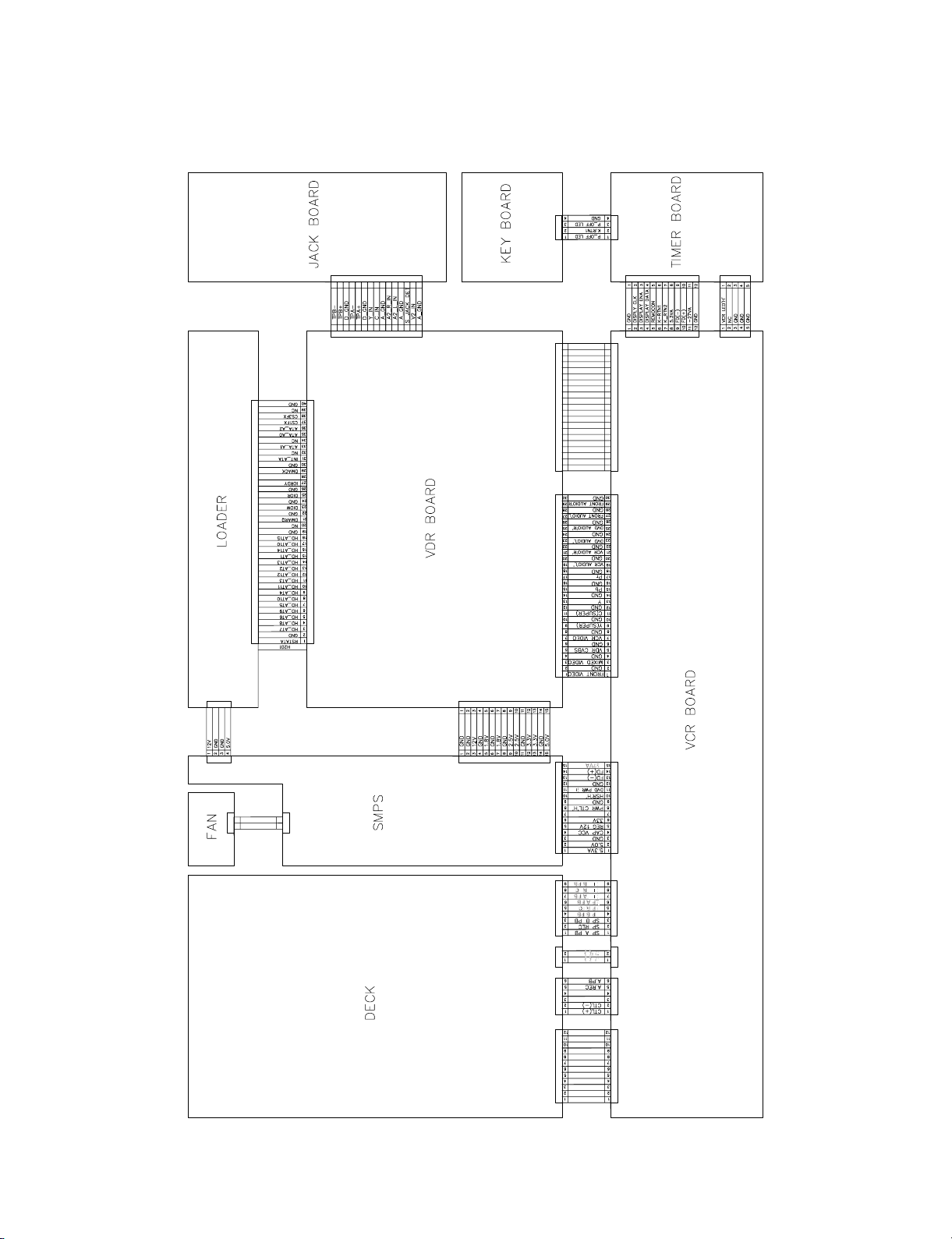
OVERALL WIRING DIAGRAMS
Page 14
3-3
ELECTRICAL ADJUSTMENT PROCEDURES
1. Servo Adjustment
1) PG Adjustment
• Adjustment And Specification
• Test Equipment
a) OSCILLOSCOPE : NTSC SP TEST TAPE
MODE
PLAY
• Adjustment Procedure
a) Insert the SP Test Tape and play.
b) Connect the CH1 of the oscilloscope to the H/SW and CH2 to the “VCR VIDEO” TP for the VCR.
c) Trigger the mixed Combo Video Signal of CH2 to the CH1 H/SW, and then check the distance (time dif-
ference), which is from the selected A(B) Head point of the H/SW signal to the starting point of the vertical synchronized signal, to 6.5H ± 0.5H (416µs, 1H=64µs).
• PG Adjustment Method
a-1) Playback the SP standard tape
b-2) Wait for 3seconds with F/P “REC” key and “PLAY” key presseed at the same time. < Digitron[ - - ] >
c-3) Repeat the above step(No.b-2), then it finishes the PG adjusting automatically. < Digitron[ PG ] >
d-4) Stop the playback, then it goes out of PG adjusting mode after mony the PG data.
• CONNECTION
• WAVEFORM
V.Out
H/SW(TP)
R/C TRK JIG KEY 6.5 ± 0.5H
MEASUREMENT POINT ADJUSTMENT POINT SPECIFICATION
H/SW
(TP)
TP
(VCR
VIDEO)
(CH2)
(CH1)
OSCILLOSCOPE
CH1 CH2
R/C KEY
H/SW
(TP)
VCR BOARDVDR BOARD
"VCR VIDEO" TP
VCR PART
H/SW
Composite
VIDEO
6.5H(416µs)
Page 15
3-4
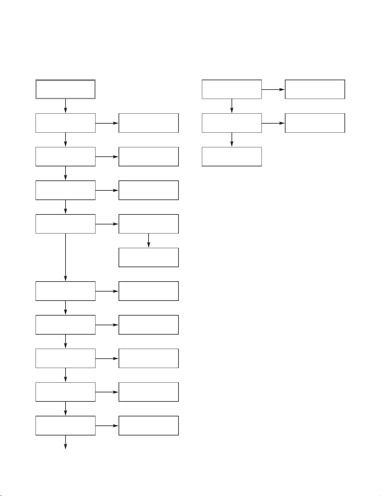
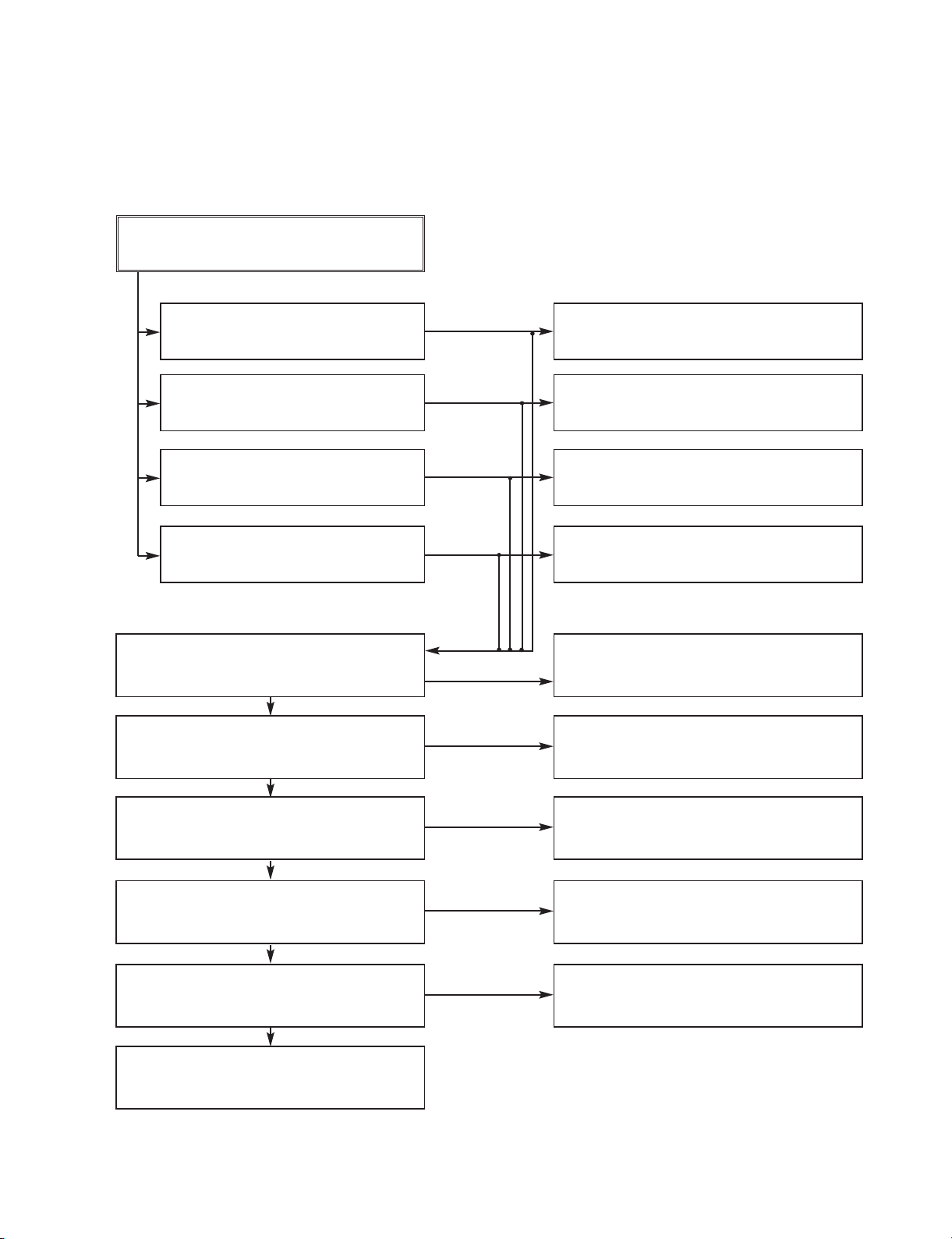
VCR ELECTRICAL TROUBLESHOOTING GUIDE
1. Power(SMPS) CIRCUIT
NO 5.3VA.
Replace the F101
(Use the same Fuse)
Is the F101 normal?
Is the TH01
Normal?
Is the BD101
Normal?
NO
NO
NO
NO
NO
NO
NO
NO
NO
NO
NO
Replace the BD101
Replace the TH01
Is the D102
normal?
Check or Replace
the D102
Replace the D121
Replace the IC103
Replace the D126
Replace the D129
Replace the D130
Replace the D127
Replace the D128
YES
YES
YES
YES
YES
YES
YES
YES
YES
YES
Is the Vcc (14V - 17V)
supplied to IC101 Pin7?
NO
Is the D121
normal?
Is there about 2.5V
at the IC103 Pin1?
Is the D126
normal?
Is the D129
normal?
Is the D130
normal?
Is the D127
normal?
Is the D128
normal?
YES
Power Line of Main
PCB(VCR) is short
Page 16
3-5
VCR ELECTRICAL TROUBLESHOOTING GUIDE
No 12VA
Check or Replace
the D126
Is the Vcc(13V)
supplied to C130?
Check or Replace
the Cap / Drum
Is the D132
Normal?
NO
NO
Replace the D132
YES
YES
(To Cap, Drum Motor )
No REG 12V
Check or Replace
the D126
Check the ‘PWR CTL
“H”’signal from µ-com
Check the 33V Line
Replace the Q126
Is the Vcc(13V) supplied to Q126Collector?
Is the Vcc(33V) supplied to Q126 Base?
Is the Q126 Nomal?
Check or Replace
the D126
NO
NO
NO
YES
YES
YES
NO VFD
Check or Replace
the R107
Is the R107
Normal?
Is the D128
Normal?
NO
Check or Replace
the D128
Check or Replace
the ZD151
NO
NO
YES
Is the ZD151
Normal?
Check or Replace
the D127
YES
YES
No 33V
Check or Replace
the D130
Is the Vcc(33V) supplied to Q123 Emittor?
Is the Q123 Base
‘H’?
NO
Check the ‘PWR CTL
“H”’signal from µ-com
NO
YES
Check or Replace
the Q123
YES
Page 17
3-6
VCR ELECTRICAL TROUBLESHOOTING GUIDE
No 28V (HSR)
Check or Replace
the D129
Is the Vcc(30V) supplied
to Q120 Collector?
Is the Vcc(33V) supplied
to Q121 Collector?
Is the Vcc(30V) supplied to Q120 Base?
NO
NO
Check or Replace
the ZD153
NO
Check the ‘HSR “H”
signal from µ-com
Check or Replace the
Q121/Q122 & 33V line
YES
YES
Check or Replace
the Q120
YES
Page 18
3-7
2. SYSTEM/KEY CIRCUIT
(1) AUTO STOP
(2) The unstable loading of a Cassette tape
Auto Stop
Does the H/SW waveform
appear at IC501 Pin18?
Do the T-UP Reel Pulses
appear at IC501 Pin80?
Is 12V applied to PMC01
Pin8?
Check the Drum Motor
signal.
Check the Power Circuit.
Check the power.
Is 5.0V applied to the
R531?
Refer to SMPS 5.3VA
troubleshooting.
Check IC501
Pins22, 23, 24, 25.
Does 5.0V appear at the
RS501?
Replace the T/UP Reel
Sensor (RS501).
Check the CST SW and
the peripheral circuitry.
Replace the IC501.
The unstable loading of a
Cassette tape
Does the “H” signal appear
at IC501 Pin58 during
inserting the CST ?
Does the “L” signal appear
at IC501 Pin10 while
inserting the CST?
Check the Deck
Mechanism.
Note :
Auto stop can occur because Grease or Oil has dried up
YES
YES YES
YES
YES
YES
NO
NO
NO
NO
NO
NO NO
YES
VCR ELECTRICAL TROUBLESHOOTING GUIDE
Page 19
3-8
3. SERVO CIRCUIT
(1) Unstable Video in PB MODE
Does the Noise level of the
screen change
periodically?
Do the CTL pulses appear
at IC501 Pin97?
Is adjusting the height of
the CTL Head accurate?
Readjust the height of the
CTL Head.
Replace the IC501.
Refer to “When the Y signal
doesn’t appear on the
screen in PB Mode”.
Does the CFG waveform
appear at the IC501 pin87?
On tracking, do the CTL
pulses move?
Does the Video Envelope
waveform appear at IC501
Pin9?
Replace IC501.
YES
YES
YES
NO NO
NO
NO
(2) When the Drum Motor
(2) doesn’t run.
Do the DFG Pulses appear
at PMC01 Pin11?
Replace the Cap M.
Aren’t the foil patterns and
the Components between
IC501 Pin 90 and PMC01
Pin11 shorted?
Replace the IC501.
Refer to “(2)
No 12VA of Power section”
Do the Drum PWM Pulses
appear at IC501 Pin76?
Aren’t the foil patterns and
the Components between
IC501 Pin76 and PMC01
Pin12 shorted?
Do the DFG Pulses appear
at IC501 Pin90?
Do the Drum PWM Pulses
appear at IC501 Pin76?
Are the connecting patterns and the Components
between IC501 Pin76 and PMC01 Pin12 shorted?
When the Drum Motor
doesn’t run,
Does 12V appear at
PMC01 Pin8?
Does 2.8V appear at
PMC01 Pin12?
Check the connector
(PMC01) and the Drum
Motor Ass’y.
NO
YES
YES
YES
NO
NO
NO
NO
NO
YES
YES
YES
VCR ELECTRICAL TROUBLESHOOTING GUIDE
Page 20
3-9
Does the CFG signal appear at
PMC01 Pin1?
Does the PWM signal appear at IC501
Pin77?
Does 2.8V appear at PMC01 Pin9?
Check the PMC01 and the Capstan
Motor Ass’y.
Does the Capstan PWM signal appear at
IC501 Pin77?
Aren’t the foil patterns and Components
between IC501 Pin77 and PMC01
Pin9 short?
Does the CFG signal come into IC501
Pin87?
Aren’t the foil patterns and Components
between IC501 Pin77 and PMC01
Pin9 short?
2. SERVO CIRCUIT
(3) When the Capstan Motor doesn’t run,
NO
NO
NO
YES
YES
YES
When the Capstan Motor doesn’t run,
Does 12VA appear at PMC01?
YES
Replace the IC501.
YES
NO
NO
YES
Refer to “SMPS(CAPSTAN/12Volt)
Trouble Shooting”.
Aren’t the foil patterns and component
between IC501 Pin87 and PMC01
Pin1 shorted?
Check the Capstan Motor Ass’y.
NO
VCR ELECTRICAL TROUBLESHOOTING GUIDE
Page 21
3-10
Keys do not work
Is 5V applied to IC501
Pin99?
Does FLD change when
a function button is
pressed?
Refer to “SMPS 5.3VA
Trouble Shooting”.
Replace the defective
switches.
YES
NO
NO
2. SERVO CIRCUIT
(4) Keys do not work
VCR ELECTRICAL TROUBLESHOOTING GUIDE
Page 22
3-11
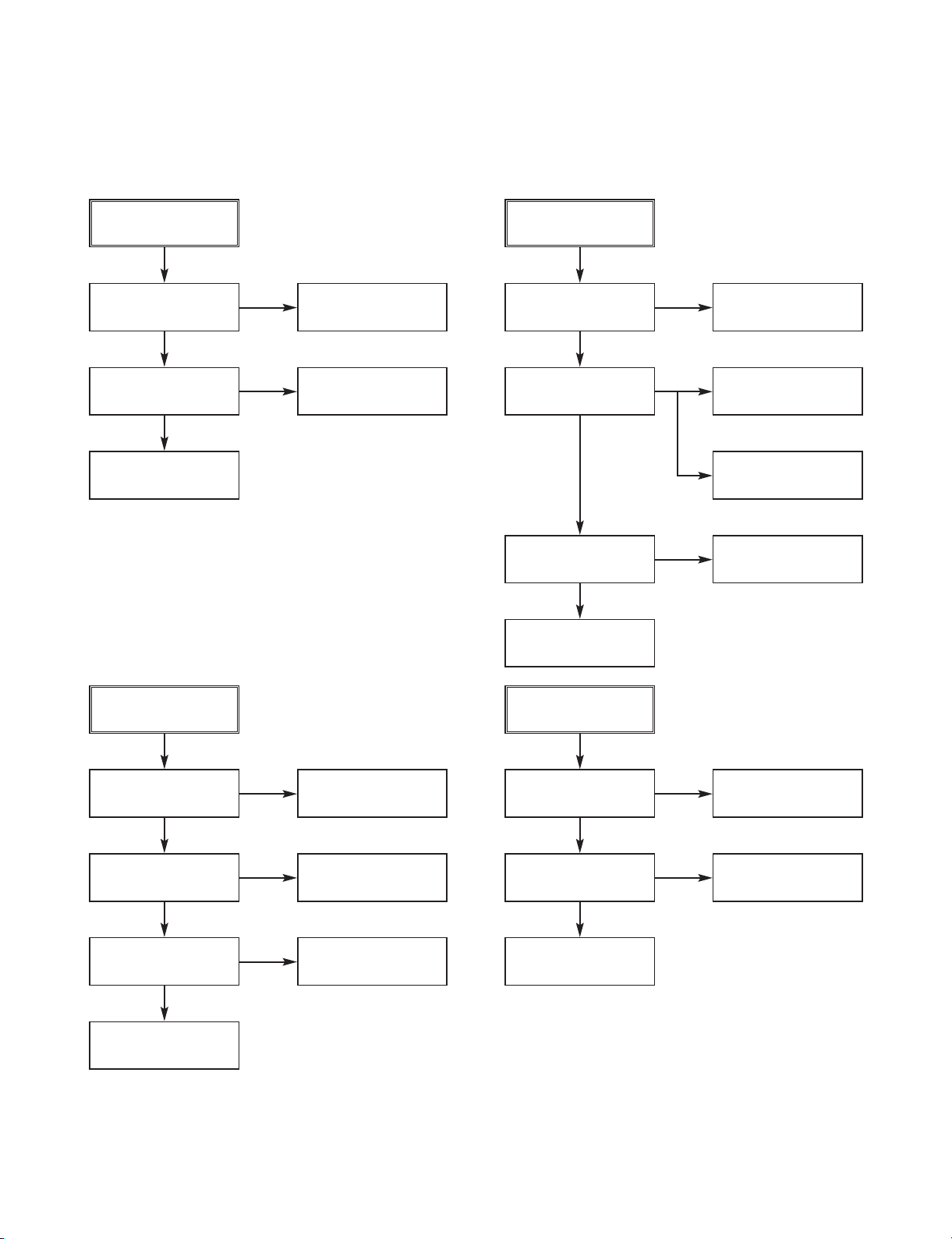
4. Y/C CIRCUIT
(1) No Video in EE Mode,
No Video in EE Mode
Does the Video signal
appear at IC301 Pin15?
Check the Tuner Part
Is REG 5.0V applied to
IC301Pins4, 22, 47, 50, 52,
60, 84, 92?
Does the Video signal
appear at IC301 Pin29?
Does the Video signal
appear at the PMD02
Pin7?
Does the Video signal
appear at the PMD02
Pin5?
Check the 5.0V, 5.3VA
Line. (Power Circuit)
Is I2C BUS signal applied to
the IC301 Pins73, 74?
Check C327. (AGC)
Replace IC301.
Check the Video Buffer
Q310, Q605.
Check the DVD Board
Video path.
Check the System Circuit.
(Refer to ‘SYSTEM I2C BUS
CHECK Trouble Shooting’)
YES
YES
YES
YES
YES
YES
YES
NO
NO
NO
NO
NO
Does the Video signal
appear at the IC601
Pin4?
Check PMD02 Pin5 and
IC601 Pin4
YES
NO
NO
Replace IC601?
VCR ELECTRICAL TROUBLESHOOTING GUIDE
Page 23
3-12
3. Y/C CIRCUIT
(2) When the Y(Luminance) signal doesn’t appear on the screen in PB Mode,
Is 5.0V 5.3VA applied to IC301
Pins22, 47, 50, 52, 60, 84, 92?
Is I2C BUS signal applied to
the IC301 Pins73, 74?
Does the normal RF signal
appear at IC301 Pin76?
Check the line of the 5.0V
5.3V Line. (Power Circuit)
Check the System Circuit.
(IC501 Pin23)
Check the V.H.S/W level.
(Check R342)
Refer to ‘SYSTEM I2C
BUS CHECK Trouble
Shooting’.
Is the V.H.S/W signal
applied to IC301 Pin80?
Is the V.H.S/W “H” about
3.4V at the IC301 Pin80?
Clean the Drum.
Check the path of the
Y(Luminace) RF signal.
Does the Y(Luminance)
RF signal appear at
IC301 Pin33?
Is the Y(Luminance) Video
waveform showed up at
IC301 Pin43?
Replace IC301.
NO
YES
YES
YES
YES
YES
YES
YES
NO
NO
NO
NO
NO
NO
Replace the IC301.
NO
VCR ELECTRICAL TROUBLESHOOTING GUIDE
Page 24
3-13
3. Y/C CIRCUIT
(3) When the C(Color) signal doesn’t appear on the screen in PB Mode,
Is 5.0V 5.3VA applied to the IC301
Pins22, 47, 50, 52, 60, 84, 92.
Does the Color signal
appear at IC301
Pin29?
Check the line of the 5.0V
5.3VA Line. (Power Circuit)
Replace the X301.
Check the Color Pass.
Does the X301
(3.58MHz) osxillate?
Replace the IC301.
Does the Color signal
appear at IC301 Pin42?
Replace the IC301.
NO
YES
YES
YES
NO
NO
NO
VCR ELECTRICAL TROUBLESHOOTING GUIDE
Page 25
3-14
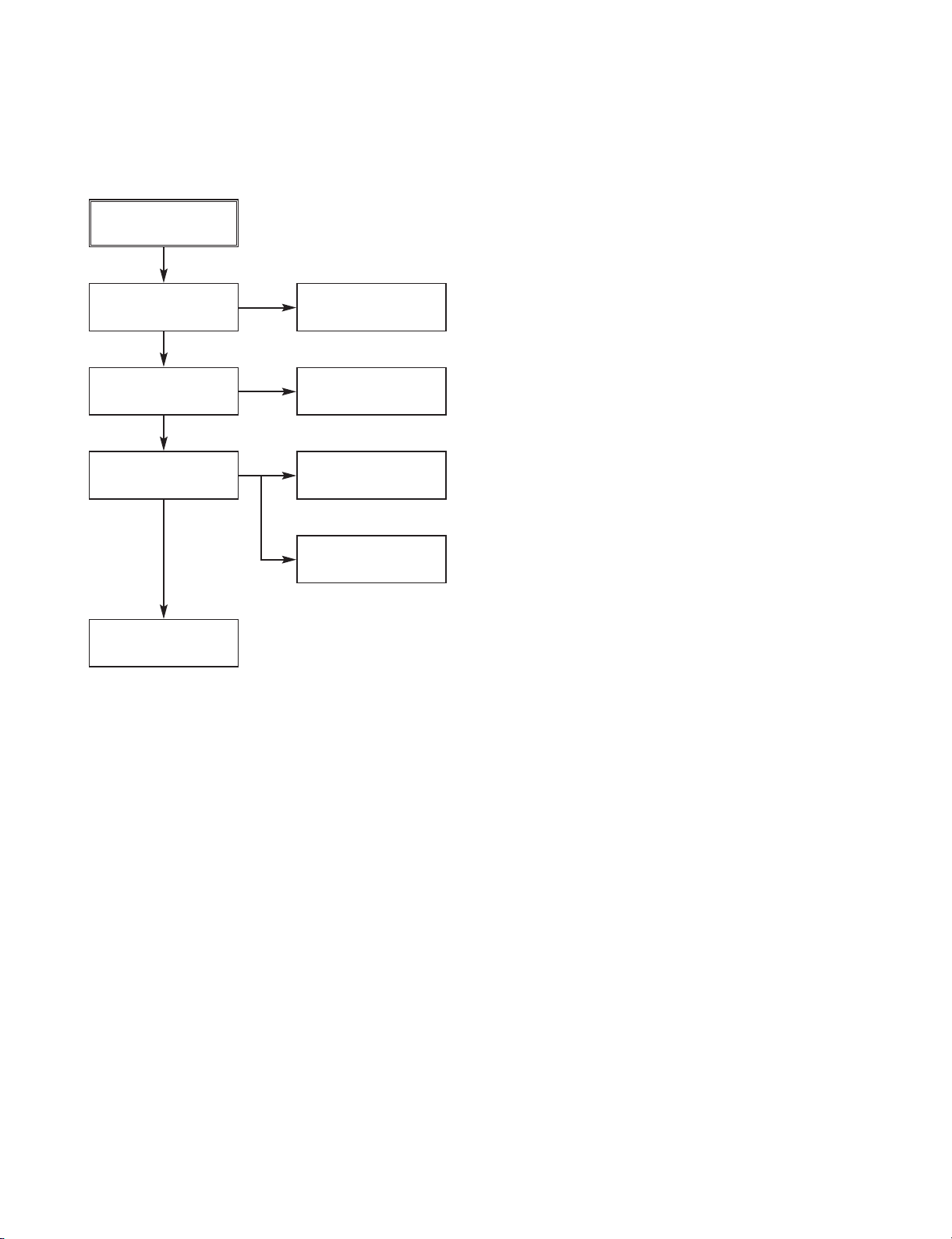
3. Y/C CIRCUIT
(4) When the Video signal doesn’t appear on the screen in REC Mode,
VCR ELECTRICAL TROUBLESHOOTING GUIDE
Is the EE signal normal?
Does the RF signal
appear at the IC301
Pin76?
Check EE Mode.
Check the System of REC
‘H’.(the IC501 Pin74)
Replace the IC301.
Is the REC ‘H’ signal
(about 4V) applied to the
OSC?
Check the circuit of the
IC301 Pin86, 90.
Check REC Luminace
pass & Color pass.
Does the REC RF signal
appear at the IC301
Pins86, 90?
NO
YES
Is 5.0V 5.3VA applied to
the IC301 Pins22, 47, 50,
52, 60, 84, 92?
Check the line of the 5.0V
5.3VA line. (Power Circuit)
NO
YES
Does PB Mode operate
nomally?
NO
Check PB Mode.
YES
Check the Drum & Drum
Connector
YES
YES
YES
NO
NO
NO
NO
Page 26
3-15
VCR ELECTRICAL TROUBLESHOOTING GUIDE
5. Hi-Fi CIRCUIT
(1) No Sound(EE Mode)
YES
No Sound.
Check the DVD Audio of IC801
Pins2, 4.
Check the 74 Audio of IC801
Pins48.
Check the Vcc of IC801 Pins25, 40, 51,
58.
YES
Check the IIC Clock and DATA at
IC801 Pins42, 43.
YES
YES
Check the Audio of IC801 Pins53, 57.
Check the SC901, JK601.
Check the DVD Audio out.
NO
Check the Tuner Part
NO
Check the Power 5.0V, 12V.
YES
NO
Check the IC501 Pins71, 72.
NO
Replace IC801.
NO
Check the Audio of PMD02 Pin19, 21.
Check the Pcb Pattern between IC801
Pin53, 57 with PMD02 Pin19, 21.
NO
YES
YES
Check the Audio of PMD02 Pin23, 25. Check the DVD Board Audio path.
NO
Check the AV1 Audio of IC801
Pins9, 14.
Check the AV1 Jack.
NO
Check the AV2 Audio of IC801
Pins10, 15
Check the AV2 Jack.
NO
Page 27
3-16
VCR ELECTRICAL TROUBLESHOOTING GUIDE
3. Y/C CIRCUIT
(2) Hi-Fi Playback
YES
YES
YES
YES
YES
NO
YES
NO
PB mode
No Sound.
Check the Vcc of IC801
(Pins25, 40, 51, 58)
Check the Hi-Fi Selection switch.
(IC801 Pin41) and the Tape quality.
Is the RF Envelope at IC801
Pin30 over 300mVp-p?
Check IC801 Pin42(Data),
Pin43(Clock)
YES
Do Audio Signals appear at
IC801 Pin22(L-CH), 24(R-CH)?
YES
Do Audio Signals appear at
IC802 Pin53(L-CH), 57(R-CH)?
YES
Check the Audio of
PMD02 Pins19, 21
YES
Check the Audio of
PMD02 Pins23, 25
YES
Check the JK601
Check Power 5.0V, 12V.
NO
Check IC501 Pin27
(A.H/SW)
NO
Is Pin29 of IC801 over
3.5V
Check Rec ‘H’ signal of
µ-com.
NO
Is the head Switching signal
IC801 Pin27 ok?
YES
Is the head Switching signal
IC801 Pin27 ok?
Check the parts of µ-COM
(IC501 Pins17, 18)
NO
Check the Connection at
P3D01 Pins7, 9.
NO
Replace IC801.
NO
Check the PCB pattern between IC801
Pins3, 5, 7 with PMD02 Pins19, 21
NO
Check the DVD Board
Audio Part
NO
Page 28
3-17
(3)
Hi-Fi REC.
It can’t be recorded Hi-Fi Audio
signal.
Check Vcc of IC801. (Pins25, 40, 51, 58)
YES
YES
Check IC801 Pin42(Data), Pin43(CLOCK).
YES
Do Audio signals appear at IC801
Pins53, 57?
YES
Do FM Audio signals appear at IC801
Pin36?
YES
Check the Contact Point of Drum
Connector if good then Replace the Drum.
YES
Check Power 5V, 12V.
NO
Check ports of µ-COM.
(IC501 pins 71, 72)
Check Audio input signal of IC801
Pins2, 4, 9, 10, 14, 15, 48.
NO
Replace IC801.
NO
NO
VCR ELECTRICAL TROUBLESHOOTING GUIDE
Page 29
3-18
VCR ELECTRICAL TROUBLESHOOTING GUIDE
7. Tuner/IF CIRCUIT
(A)
No Video on TV screen.
Is Tuner mode selected?
YES
changer to Tuner mode using remocon.
NO
Is “TV” displayed on FLD displayed
YES
Is +5V applied to TU701 Pin 3?
NO
Is “High” applied to TU701 Pin 4?
YES
Does the Video signal appear at Pin 16
of TU701?
YES
Replace TU701
YES
Set TV/VCR SW to VCR using remocon.
YES
Check 5V Line.
NO
Check the voltage at Pin26 of IC501.
(“H” for tuner mode)
NO
Check the path form Pin23 of IC601
to the Pin 5 of TU701.
NO
Page 30
3-19
VCR ELECTRICAL TROUBLESHOOTING GUIDE
(B)
No TV sound.
Check the Vcc of IC801(Pin58).
YES
Check Power (Vcc 12V)
NO
Check IC801 Pin 43(DATA),
Pin 42(CLOCK) “HIGH”?
YES
Check IC801 Pin 48(TUNER SIF).
NO
Replace IC801.
YES
Check IC501 Pin 71(CLOCK),
Pin 72(DATA)
YES
Check TU701 Pin 13
(TUNER Audio Output)
NO
Page 31

Page 32

3-20 3-21
BLOCK DIAGRAMS
1. POWER(SMPS) BLOCK DIAGRAM
BD
101
!
NOISE FILTER
BLOCK
(C101,L102,
L101, C102)
!
FUSE
(F101)
BR BL
(BK)(WH)
!
Y-CAP
C110
TH0
1
C103
S/W Block
(Q111
)
!
+
Y-CAP
C111
!
T101
SNUBBER
BLOCK
(D101,C105
C106,R103)
DRIVE & S/W BLOCK
(IC101, D102, R105,
C108,C112,C120,
ZD101
)
PHOTO COUPLER
(IC107
)
SNUBBER
BLOCK
(D103,C115,C116
,R112,R115)
DRIVE & S/W BLOCK
(IC104, D104, R113,
C117,C114,C119,
ZD102)
(D126,C136,L122,C130
PHOTO COUPLER
!
!
!
(IC102
2
T10
PHOTO COUPLER
(IC105
RECTIFIER &
SMOOTING BLOCK
(D128,C133,R130)
RECTIFIER &
SMOOTING BLOCK
RECTIFIER &
SMOOTING BLOCK
(D129,C128,R147)
RECTIFIER &
SMOOTING BLOCK
(D130,C137,R146)
RECTIFIER &
SMOOTING BLOCK
(D121,C122,L121,C124)
FEED-BACK
)
ERROR AMP
(IC103)
RECTIFIER &
SMOOTING BLOCK
(D125,C139,L127,C140)
RECTIFIER &
SMOOTING BLOCK
(D124,C129)
RECTIFIER &
SMOOTING BLOCK
(D123,C126,L124,C127)
RECTIFIER &
SMOOTING BLOCK
(D122,C123,L123,C125
)
ERROR AMP
(IC106)
BLOCK
R121,R122,
C121,R123.
R124.R125
R126
FEED-BACK
BLOCK
R131,R132,
C141,R133.
R161.R162
R163
RECTIFIER &
SMOOTING BLOCK
(D127,C131,L125,C132)
)
HSR S/W Block
(Q120,ZD153,C135,
R144,R145,D155,C157)
TO VCR
(P101)
5.3VA
5.0V
C
ap Vcc
REG 12V
33V
12V REG & S/W Block
(Q126,R150,ZD152,
C156,C153)
33V S/W Block
(Q123,R143,R134
)
12VA(DRUM)
PWR CTL 'H'
HSR 'H'
DVD PWR CTL
FD(-)
5.0V S/W Block
(Q124,R140,R135,R136
D134,C134
HSR CTL Block
(Q121,Q122,R141)
)
PWR CTL Block
(Q125,R137,R138
12V REG & S/W Block
(IC157,R156,C155)
)
)
FD(+)
-28VA
TO FAN
(P104)
8.7V
TO VDR
(P102)
-12V
12V
V
5.0V REG & S/W Block
(IC151,R151,C151)
1.8
2.5V
3.3V
1.8V REG & S/W Block
(IC160,R159,C152,
R167,R168)
)
3.3V REG & S/W Block
(IC154,R154,C154)
5.0V
TO LOADER
(P103)
12V
5.0V
2.5V REG & S/W Block
(IC152,R169,C150
)
)
Page 33

3-22 3-23
2. AVCP BLOCK DIAGRAM
1) PB Mode
2) REC Mode
System
System
System
(FROM u-COM)
CLOCK
(FROM u-COM)
DATA
VCO/OSC
interface
L-DET
VCD
(-4dB)
SP CH2
85
REC-AMP
APC/ACC
V. OUT
D-V SYNC
(FROM u-COM)
29
MIX
AMP
DET
APC/ACC
Main
Conv2
CCD LPF
VCA
28
SQUEL CH
C.K
BDBPF
L- DET
C LPF DEALY
fh Trap
HIFI Trap
CTL Trap
ACC
2M LPF
CLEAR
Main
SYNC
Conv1
CLAMP
NL
De-eMPH
Main
De-Empf
S LPF
DEMO
FM AGC P.EQ G.EQ D LIM Y LPF
TRAP
50
SYNC SEP
30
FBC
Video ALC
Sharpness
CONTROL
YNR NC
CLAMP
LPF
LPF
+
+
3640383723 26
System
DATA
System
98
18
CLOCK
51
49
53
55
CLOCK Drive
interface
VCO/OSC
Y-CCD
C-CCD
57 45 46
73 6574
Serial Cont
X-tal
68 71
79 78
V.H/SW30
System
80
(FROM u-COM)
(FROM u-COM)
57 7365 74 6867
45
(FROM u-COM)
X-tal
Serial Cont
IC301
HA118725NF
IC301
SP CH1
SP CH2
REC-AMP
REC-AMP
80
85
83
86
87
REC-AMP
899190
EP CH2
EP CH1
REC-AMP
HA118725NF
46
C-CCD
CLOCK Drive
49
53
55
86
SP CH2
REC
f0=1.68M
MIX
B.E
LPF
CCD
C-LPF
Main
Conv2
DET
Y-CCD
11
LPF
SPFACC
Trap
ATT
C.K
SP CH1
87
SP CH1
REC-AMP
C-LPF
Main
Conv2
6dB
AMP
29
VCA
TRAP
HPF
LPF
FM
MOD
Main
Emph
ALC
FBC
NL Emph
D.E.
CLEAR
SQUEL CH
28
89
SYNC
EP CH2
90
EP CH2
REC-AMP
Adjst
f/0DEV
FBC
Video ALC
Y-LPF
EP CH1
EP CH1
REC-AMP
YNR
AGC
VIDEO
91
SYNC
AGC DET
SEP
CLAMP
CLAMP
LPF
ATT
ATT
ATT
-10dB
-10dB
-10dB
2HD Model Only
4HD/4HD Hi-Fi Model Only
17 19 18 36 40 38 37 51 36 30 32 9 8 11
15
++++
+
+
VIDEO IN
S/W
DVD
VIDEO IN
TV
V.ENV
V.H/SW30
(FROM u-COM)
System
4HD/4HD Hi-Fi Model Only
2HD Model Only
(TO u-COM)
SP CH2
SP CH1
EP CH2
EP CH1
V. OUT
D-V SYNC
Page 34

3-24 3-25
3. SYSTEM BLOCK DIAGRAM
TO/FROM AVCP
TO/FROM DECK
TO/FROM AUDIO(Hi-Fi)
TO/ FROM TU/IF
5V
TO/FROM DECK
MODE S/W
T-UP END
ES501
R550
LD501
DECK IR LED
R553
R555
R557
RS501
T-UP REEL
5.3VA
MS501
To/FROM DVD
SUP END
R556
RS502
SUP REEL
CST.SW/REC TAP
R531
CS501
5.3VA
GND
MODE S1
MODE S2
MODE S3
MODE S4
ES502
R564
R538
R558 C582
R544
X501
32.768KHz
R535
R537
X502
14MHz
OSC
OSC
R536
R5C6
C534
C552
C535
I-Limit
25
MODE S1
24
MODE S2
23
MODE S3
22
MODE S4
62
VDR ENA
66
VDR DATA
65
VCR DATA
67
VCR ENA
38
X in
39
X out
Xc in
35
Xc out
36
21
T-UP Sensor
20
SUP Sensor
80
T-UP Reel
79
SUP Reel
CST IN
58
14
R/C
RC601
11
76
94
95
77
CAP. PWM
CTL -
CTL +
DRUM PWM
12 59
87
90
CFG
DPG
IC501
M37760
LD CTL
CAP. REV 'H'
Vss (OSD)
Vss (AMP)
49
88
9
18
13
V. ENV
V.H.SW30
Vss (SYSCON)
Vcc (A/D)
40
99
16
H.A.SW
REC 'H'
D.V.Sync
A.MUTE'H'
FLD DATA
FLD ENA
FLD CLK
A. H.SW
A. MUTE 'H'
REC 'H'
IIC CLK
IIC DATA
CV OUT
IIC CLK
IIC DATA
POWER FAIL
Vcc (OSD)
Vcc
53
98
50
17
74
15
C.ROT
84
68
69
70
8
A. ENV
19
68
74
71
72
52
100
AFT
71
72
26
VCR 'H'
78
34
Vcc
(SYSCON)
(SERVO)
RESET
37
+ +
C500 C517
CV IN
COMP IN
C592
TO/FROM AVCP
DISPLAY
IC5F1
TO/FROM AUDIO(Hi-Fi)
TO/ FROM TU/IF
+
+
R541
R529
C503
Q503
Q501
R583
L512
5.3VA
5V
3
3
IC504
Vcc
1
IC505
Vcc
1
GND
2
GND
2
+
C561
L501
LGXBR446 (LGEUS)
Page 35

3-26 3-27
4. JACK BLOCK DIAGRAM
To.AVCP
To.AVCP
From
AVCP
PMD02
1) Front Video
3) Mixed Video
5) VDR CVBS
7) VCR Video
9) Y (Super)
11) C (Super)
19) VCR A-L
21) VCR A-R
23) VDR A-L
25) VDR A-R
27) Front A-L
29) Front A-R
13) Y
15) Pb
17) Pr
VIDEO SW IC
7
3 5 1
IC601
IC601
VIDEO AMP IC
4
6 21
2 26
10 20
12 18
14
From PMD01 Pin
23
16
IEC-958
1
To Hi-Fi
To TUNER
MOD VIDEO
JK601
A/V JACK
AV1 Video in
AV1 Audio in
(L/R)
Video Out
Y Out (Super)
C Out (Super)
Y Out (Comp)
Pb Out (Comp)
Pr Out (Comp)
Audio Out L
Audio Out R
Coaxial Out
From/To Hi-Fi IC801
JK603
Optical Jack
LGXBR446 (LGEUS)
Page 36

3-28 3-29
5. STUNER/MTZ BLOCK DIAGRAM
A.IN
CH S/W
REG 5V
CONTROL
V.IN
RF AGC
NC
ENABLE
CLOCK
DATA
AFT
A.OUT
SIF
TU 30V
NC
V.OUT
11
10
1
2
3
4
5
6
7
8
9
716 MOD A.IN
61 MOD CTL
106 5V
26 VCR 'H'
671 MOD VEDIO
71 IIC CLK
72 IIC DATA
781 SIF OUT
12
13
14
15
16
999 GND
731TU.V.OUT
45833V
100AFT
LGXBR446 (LGEUS)
Page 37

3-30 3-31
6. AVCP BLOCK DIAGRAM
1) EE Mode
2) PB Mode
3) REC Mode
A. OUT (L)
57
IC801
AN3662(AN3663)
A. OUT (R)
53
OUTPUT
SELECTOR
626
VCA
73 74
(System)
From u-COM
DATA
CLOCK
A. OUT (L)
57
IC801
AN3662(AN3663)
A. OUT (R)
53
OUTPUT
SELECTOR
626
VCA
73 74
(System)
From u-COM
DATA
CLOCK
DET
IC301
HA118725NF
IC801
AN3662(AN3663)
VCA
2
NORMAL
AUDIO
OUT
61
6
62
98
REC
AMP
DVD
A.OUT'L'
A.OUT'R'
53
57
15
10
14
9
IC301
HA118725NF
EQ
AMP
95
96
N.A.IN
/P HEAD
EQ
94
IC301
HA118725NF
EQ
AMP
95
96
N.A.IN
/P HEAD
EQ
94
TU701
TUNER
18 48
OUT
AUDIO
2
4
DVD'L'
DVD'R'
LINE 1 'L'
LINE 2 'L'
LINE 1 'R'
LINE 2 'R'
Page 38

3-32 3-33
A B C D E F G H I J K L M N O P Q R ST
30VA No Power
D130 is Defective
No Power
BD101,TH01 is Defective
-28VA No Power
D127 is Defective
No Power
D102 is Defective
5.3VA No Power
D121 is Defective
Switching Error
IC102,IC103 are Defective
No Power
F101 is Defective
3.3V No Power
D122 is Defective
Switching Error
IC105,IC106 are Defective
S/W Error
IC107,Q111 is Defective
12V No Power
D125 is Defective
28V No Power
D129 is Defective
12V No Power
D126 is Defective
12V No Power
Q125 or ZD152 are Defective
12V No Power
IC157 is Defective
2.5V No Power
IC152 is Defective
5V No Power
IC151 is Defective
1.8V No Power
IC160 is Defective
3.3V No Power
IC154 is Defective
5V No Power
D124 is Defective
1.8V No Power
D123 is Defective
No Digitron Displayed
D128,R107,ZD151 are Defective
S/W Error
IC101,IC104 is Defective
28V No Power
Q120 or ZD153 are Defective
NOTES) Symbol denotes AC ground.
NOTES) Symbol denotes DC chassis ground.
NOTE) Warning
NOTE) Parts that are shaded are critical
NOTE) With respect to risk of fire or
NOTE) electricial shock.
CIRCUIT DIAGRAMS
1. POWER(SMPS) CIRCUIT DIAGRAM
IMPORTANT SAFETY NOTICE
WHEN SERVICING THIS CHASSIS, UNDER NO CIRCUMSTANCES SHOULD THE ORIGINAL DESIGN BE
MODIFIED OR ALTERED WITHOUT PERMISSION
FROM THE LG ELECTRONICS CORPORATION.
ALL COMPONENTS SHOULD BE REPLACED ONLY
WITH TYPES IDENTICAL TO THOSE IN THE ORIGI-
NAL CIRCUIT. SPECIAL COMPONENTS ARE SHADED
ON THE SCHEMATIC FOR EASY IDENTIFICATION.
THIS CIRCUIT DIAGRAM MAY OCCASIONALLY DIFFER FROM THE ACTUAL CIRCUIT USED. THIS WAY,
IMPLEMENTATION OF THE LATEST SAFETY AND
PERFORMANCE IMPROVEMENT CHANGES INTO
THE SET IS NOT DELAYED UNTIL THE NEW SERVICE
LITERATURE IS PRINTED.
NOTE :
1. Shaded( ) parts are critical for safety. Replace only
with specified part number.
2. Voltages are DC-measured with a digital voltmeter
during Play mode.
Page 39

3-34 3-35
A B C D E F G H I J K L M N O P Q R ST
2. TUNER CIRCUIT DIAGRAM
Page 40

3-36 3-37
A B C D E F G H I J K L M N O P Q R ST
1
14
WAVEFORM
4
3
2
7
8 1312
11
2
2
2
2
3
9
10
6
3. A/V CIRCUIT DIAGRAM
Page 41

3-38 3-39
A B C D E F G H I J K L M N O P Q R ST
4. Hi-Fi CIRCUIT DIAGRAM
Page 42

3-40 3-41
1
2
7
4
3
6
5
WAVEFORM
A B C D E F G H I J K L M N O P Q R ST
5. SYSTEM CIRCUIT DIAGRAM
Page 43

3-42 3-43
A B C D E F G H I J K L M N O P Q R ST
6. JACK CIRCUIT DIAGRAM
Page 44

A B C D E F G H I J K L M N O P Q RST
3-44 3-45
7. TIMER CIRCUIT DIAGRAM
Page 45

3-46 3-47
WAVEFORMS
IC301 Pins 8, 9
PB mode
500mvp-p
IC301 Pins 15, 17,
19, 21
Video in 1Vp-p
IC301 Pin 31
PB/REC mode
4.0Vp-p
IC301 Pin 98
REC mode
1.1Vp-p
IC301 Pin 94
REC mode
2.0Vp-p
IC301 Pin 29
PB mode
2.02Vp-p
IC301 Pin 57
PB mode
400mVp-p
IC301 Pin 63
PB mode
400mVp-p
IC301 Pin 73
PB/REC mode
5Vp-p
IC301 Pin 74
PB/REC mode
5Vp-p
IC301 Pin 77
REC mode
340mVp-p
IC301 Pin 42
PB mode
300mVp-p
IC301 Pin 53
PB mode
400mVp-p
IC301 Pin 80
PB mode
3.6Vp-p
✦ IC301 Oscilloscope Waveform
✦ IC501 Waveform Photographs
V.HSW
(IC501 Pin 18)
1V/10mS
REC/PB MODE
DV.SYNC
(IC501 PIN 13)
1V/100uS
QUE/REV MODE
CTL(+)
(IC501 Pin 95)
1V/10mS
CTL(-)
(IC501 Pin 94)
1V/10mS
DFG/DFG
(IC501 PIN 90)
1V/10mS
REC/PB MODE
CFG
(IC501 Pin 87)
1V/10mS
V.IN
(IC501 Pin 49)
500mV/20uS
Page 46

3-48 3-49
1 0.06 0.06
2 0.06 0.06
3 0.06 0.06
4 0.35 0.37
5 2.35 2.09
6 2.58 2.55
7 2.83 2.83
8 1.84 1.24
9 1.84 1.23
10 2.41 1.89
11 2.61 3.00
12 1.60 0.56
13 0.00 0.00
14 2.80 2.26
15 2.80 2.38
16 0.18 1.91
17 2.79 2.80
18 1.76 1.91
19 2.80 2.80
20 0.02 0.00
21 2.80 2.80
22 5.08 5.12
23 2.32 2.34
24 0.18 0.57
25 2.12 2.12
26 3.00 2.80
27 0.18 0.45
28 0.15 0.15
29 2.48 2.46
30 2.80 2.91
31 0.37 0.37
32 2.31 2.79
33 2.09 2.13
34 1.76 1.85
35 3.03 3.07
36 2.32 2.35
37 3.03 3.06
38 2.15 2.20
39 1.42 1.45
40 2.08 2.12
41 3.01 2.55
42 1.98 1.97
43 2.05 2.05
44 0.00 0.00
45 3.13 3.15
46 3.13 3.15
47 5.03 5.07
48 0.14 0.14
49 3.17 3.19
50 5.03 5.07
51 2.05 2.07
52 5.03 5.07
53 2.62 2.64
54 0.00 0.00
EE PLAY
MODE
PIN NO.
IC301
55 2.07 2.09
56 0.00 0.00
57 2.18 2.18
58 2.34 2.34
59 4.94 4.97
60 4.94 4.97
61 0.02 0.02
62 2.28 2.21
63 2.23 2.23
64 2.94 2.95
65 2.26 2.26
66 2.95 2.96
67 2.19 2.18
68 1.28 1.24
69 1.96 1.96
70 2.71 1.42
71 2.19 2.19
72 0.14 0.14
73 5.20 5.21
74 5.20 5.21
75 2.76 2.79
76 2.25 2.17
77 2.84 2.84
78 0.02 0.03
79 0.00 0.00
80 2.54 2.53
81 4.85 4.84
82 4.15 4.15
83 0.00 2.53
84 5.07 5.10
85 2.46 2.30
86 2.54 2.30
87 2.45 2.30
88 0.00 0.00
89 2.48 2.30
90 2.52 2.30
91 2.48 2.30
92 5.08 5.11
93 0.52 0.51
94 2.53 2.54
95 2.53 2.52
96 2.53 2.50
97 0.01 0.01
98 2.27 2.55
99 0.00 0.00
100 2.58 2.55
10 0
2 4.52 4.82
3 4.84 4.84v
4 4.64 4.58v
5 4.56 4.56v
6 80m 60m
70 0
8 4.98 4.98
EE PLAY
MODE
PIN NO.
• CIRCUIT VOLTAGE CHART
9 4.98 5.30
10 4.8 4.80v
11 4.82 4.82
12 4.72v 4.82
13 4.92 4.92
14 5.02 5.02
15 0 0
16 4.98v 4.98
17 5.04 5.04
18 4.98v 9.98
19 2.46v 2.46
20 3.36V 3.36
21 0 0
22 0 0
23 4.96v 4.96v
24 120mv 140m
25 4.94 4.94
26 4.92v 4.92v
27 20m 20mv
28 5.02 5.02v
29 4.98v 4.98
30 4.84v 4.84
31 5.00v 5.00v
32 0 0
33 4.98 4.94
34 0 5.00v
35 5.02 100m
36 3.16 3.12v
37 5.7v Da/Clk(5.5)
38 0 5.7v
39 520m 0
40 4.84 520m
41 4.83 Da/Clk(5.62)
42 4.86v 4.86v
43 0 0
44 5.02 5.0v
45 0 0
46 3.94 3.94v
47 2.88 2.88v
48 0 0
49 0.98 2.94
50 1.84 1.94v
51 0.98 4.78
52 3.28 3.28v
53 2.38 2.38v
54 2.52 2.54v
55 1.88 1.88
56 0 0
57 0 0
58 120m 120m
59 4.92v 4.92v
60 4.92v 4.92v
61 0 0
62 4.82 4.82v
63 3.98 3.98v
EE PLAY
MODE
PIN NO.
64 0 0
65 2.36 2.36v
66 0 0
67 4.68 9.68v
68 0 0
69 2.48 2.48v
70 2.48 2.48
71 0 0
72 2.48 4.98
73 4.92 4.92v
74 0 0
75 2.52 2.42
76 2.42 2.48
77 80m 80m
78 0 0
79 4.02v 4.96v
80 4.96v 4.96
81 2.8 280m
82 1v 2.62v
83 120m 3.24v
84 0 1.96
85 0 0
86 4.98 4.9v
87 4.98 4.98
88 5.0v 5.0v
89 0 0
90 4.88 4.88v
91 0 0
92 0 0
93 5.04v 5.04v
94 4.88 0
95 4.98 4.98
96 0 0
97 0 0
98 4.98 4.98
99 20m 4.98v
100 0 0
1 4.88 4.88v
2 1.46 1.48
3 1.38 1.38
40 0
5 2.26v 2.24
6 2.38 0
70 0
80 0
90 0
10 0 0
11 0 5.0v
12 5.0v 5.0
13 5.0v 0
14 0 0
15 0 0
16 0 0
17 0 0
EE PLAY
MODE
PIN NO.
IC751
IC501
18 0 0
19 4.88 4.88
20 0 0
21 0 0
22 0 0
23 0 0
24 0 0
25 0 0
26 0 0
27 0 0
28 0 0
29 0 0
30 2.96v 3.98
31 2.96 3.98
32 0 0
33 4.88v 4.88
34 3.64v 3.58v
35 0 0
36 2.62v 2.58
37 0 0
38 0 0
39 0 0
40 2.54v 2.54
41 2.54 2.56
42 2.48 2.48
43 2.3v 2.34
44 0 0
10 0
20 0
3 0 142M
4 DA/CL(5.34) DA/CL(5.34)
5 DA/CL(5.34) DA/CL(5.34)
60 0
7 DA/CL(5.34) DA/CL(5.34)
80 0
9 DA/CL(5.34) DA/CL(5.34)
10 DA/CL(5.34) DA/CL(5.34)
11 0 41M
12 DA/CL(2.82) DA/CL(2.82)
13 0 0
14 DA/CL(2.82) DA/CL(62M)
15 2.89 1.41
16 1.53 950M
17 DA/CL(1.14) DA/CL(810M)
18 0 0
19 5.26 5.24
20 5.26 5.24
1 3.28 3.24
2 3.28v 3.28
3 3.32 3.26
4 3.28 3.92
5 3.28 3.92
6 3.28 3.26
EE PLAY
MODE
PIN NO.
IC7V1
IC801
7 3.28v 3.74
8 3.28 3.24
9 3.28v 3.24
10 3.28 3.24
11 3.28v 3.26
12 0 0
13 3.78 4.52
14 0 0
15 0 640m
16 5.82 6.64
17 5.28v 6.68
18 0 620m
19 6.28 6.66
20 6.28 6.72
21 4.46v 4.42
22 3.28 4.02
23 3.62 3.68
24 3.74 4.12
25 3.74 3.76
26 0.1 640m
27 0 0
28 3.7v 3.68
29 3.66 3.64
30 0.7 680m
31 3.72 3.72v
32 3.74v 4.08
33 3.62 3.68
34 13.4v 13.32
35 580m 520m
36 0 520m
37 580m 520m
38 0 0
39 0 20m
40 4.7 4.76
41 0v 1.68
42 5.0v 5.04m
43 50.v 4.96
44 20m 3.38
1 4.76 4.68
2 2.02v 2.24
3 4.88 4.88
4 1.64 1.78
5 4.72 4.78
6 1.88 1.88
70 0
8 2.26 2.18
90 0
10 1.64v 1.72
11 0 0
12 1.92v 2.08
13 4.86 4.82
14 1.92v 2.08
15 0 2.31
16 2.26v 2.64
EE PLAY
MODE
PIN NO.
IC901
17 0 0
18 2.28 2.74
19 0 0
20 2.56v 2.58
21 2.64v 2.68
22 0 0
23 2.56v 2.92
24 0 0
25 0 0
26 2.52v 2.98
27 20m 0
28 4.72 4.68
1 2.51 2.51
2 2.39 2.39
3 3.54 3.53
4 2.57 2.56
5 1.52 1.34
6 0.43 3.68
7 1.3m 0
8 1.2m 0
9 3.04 3.03
10 2.52 2.52
11 2 2.05
12 3.22 1.97
13 3.99 3.99
14 2.5 2.495
15 3.11 1.93
16 3.2 3.18
17 27.4m 4.11
18 112.1m 3.35
19 2.27 2.26
20 1.99 2.12
21 2.31 2.37
22 0.78 0.81
23 5.02 5.01
24 5.02 5
25 2.44 2.27
26 2.44 2.26
27 2.82 2.85
28 181.5m 187.4m
29 371.6m 212.2m
30 2.08 2.08
1 3 2.99
2 36.3m 38.1m
3 3.04 3.04
4 6.4m 39.1m
5 3.04 3.04
6 5.02 5.03
7 2.24 2.23
80 0
1 6.71 6.66
2 5.05 5.05
EE PLAY
MODE
PIN NO.
IC901
IC302
IC804
3 6.02 5.96
40 0
5 6 5.96
6 5.99 5.94
7 22.3m 21.3m
8 6.68 6.65
9 6.7 6.67
10 1.1m 0
11 6.71 6.68
12 5.04 5.05
13 12.03 11.99
14 6.7 6.7
15 0 0
16 6.73 6.69
1 1.3 1.3
2 4.9 4.9
3 1.66 1.56
40 0
50 0
6 4.9 4.9
7 1.7 1.6
80 0
1 1.37 1.37
25 5
3 2.18 2.17
40 0
50 0
6 5.21 5.21
7 2 2.17
80 0
EE PLAY
MODE
PIN NO.
IC902
IC903
Page 47

3-50 3-51
PRINTED CIRCUIT DIAGRAMS
1. VCR P.C.BOARD
Page 48

3-52 3-53
2. SMPS P.C.BOARD
LOCATION GUIDE
Page 49

3-54 3-55
3. JACK P.C.BOARD
LOCATION GUIDE
( BOTTOM VIEW )
4. HDD P.C.BOARD
( TOP VIEW )
Page 50

3-56 3-57
5. KEY P.C.BOARD
6. Timer P.C.BOARD
( TOP VIEW ) ( BOTTOM VIEW )
( TOP VIEW )
( BOTTOM VIEW )
Page 51

Page 52

3-58
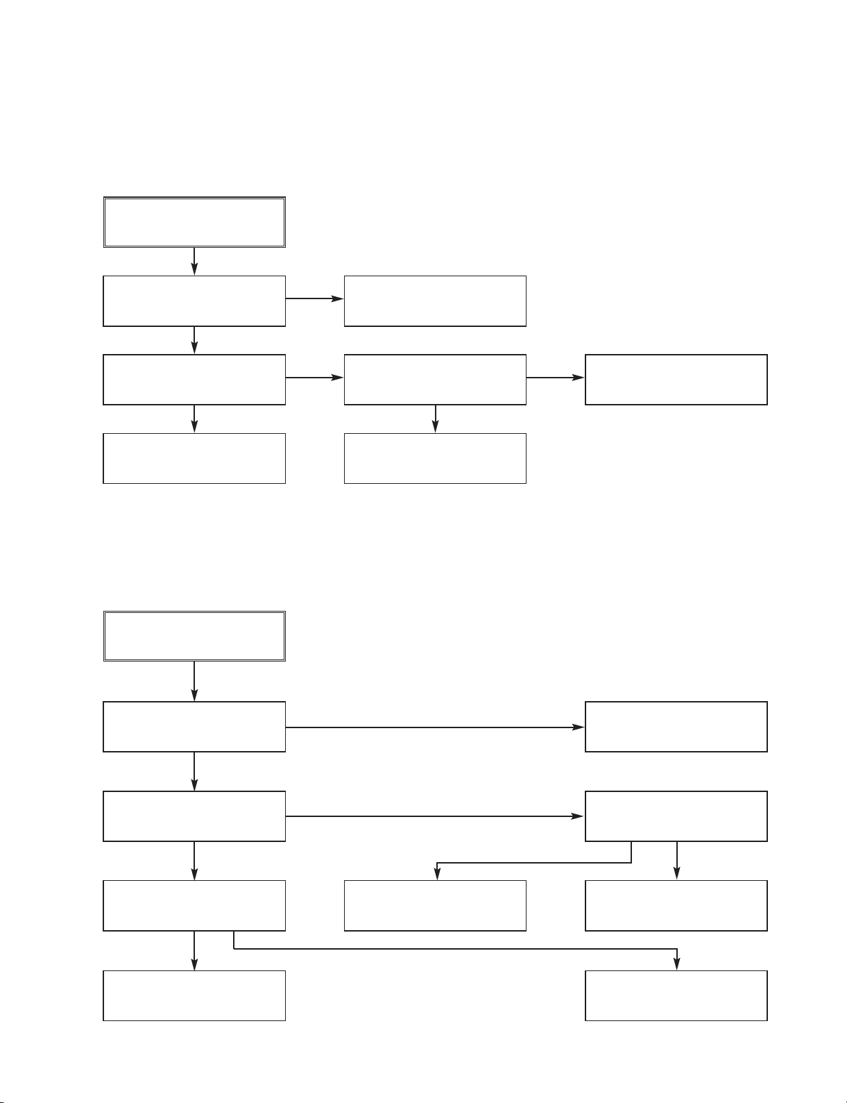
VDR ELECTRICAL TROUBLESHOOTING GUIDE
1. Power(SMPS) CIRCUIT
No 3.8VA
Replace the F101
(Use the same Fuse)
Is the F101
Normal?
Is the TH01
Normal?
Is the BD101
Normal?
NO
NO
NO
NO
NO
NO
NO
NO
NO
Replace the BD101
Replace the TH01
Is the IC107,Q111
Normal?
Check or Replace
the IC107,Q111
Replace the D122
Replace the IC106
Replace the D123
Replace the D124
Replace the D125
YES
YES
YES
YES
YES
YES
YES
YES
YES
Is Vcc (14V-17V)
supplied to IC101 Pin7?
NO
Are the D122
normal?
Is there about 2.5V
at the IC106 Pin1?
Is the D123
normal?
Is the D124
Normal?
Is the D125
Normal?
Power Line of Main
PCB(VDR) is short
VDR PART
No 3.3V
Check or Replace
the D122
Is there about 3.8V
at the IC154 pin1?
Check the IC154 and
Replace
Is there about 3.3V~ 5V
at the IC154 pin4?
NO
NO
Check the ‘DVD PWR CTL
“H”’ signal from µ-com
YES
YES
Page 53

3-59
VDR ELECTRICAL TROUBLESHOOTING GUIDE
No 2.5V
Check or Replace
the D122
Check the ‘DVD PWR CTL
“H”’ signal from µ-com
Is there about 3.8V
at the IC152 pin1?
Is there about 3.3V~
5V at the IC152 pin4?
Check the IC152
and Replace
NO
NO
YES
YES
No 5.0V
Check or Replace
the D124
Is there about 5.5V
at the IC151 pin1?
Is there about 3.3V~ 5V
at the IC151 pin4?
NO
Check the ‘DVD PWR CTL
“H”’ signal from µ-com
NO
YES
Check the IC151
and Replace
YES
No 1.8V
Check or Replace
the D123
Is there about 2.3V
at the IC160 pin1?
Is there about 3.3V ~
5V at the IC60 pin4?
NO
Check the ‘DVD PWR CTL
“H”’ signal from µ-com
NO
Check or Replace
the R167,R168
NO
YES
Are the R167,R168
normal?
YES
Check the IC160
and Replace
YES
NO
YES
No 12V
Check or Replace the
D125
Is there about 13.5V
at the IC157 pin1?
Check the IC157 and
Replace
Is there about 3.3V~
5V at the IC157 pin2?
NO
NO
Check the ‘DVD PWR CTL
“H”’ signal from µ-com
YES
YES
Page 54

3-60
2. No Component video signal when playing DISC
Component : No Y Signal Component : No Pb Signal Component : No Pr Signal
R905, C923 R904, C922 R903, C921
IC601 – 12
Check input
IC601 – 14
Check input
C907 C908
IC601 – 10
Check input
C906
FL505, FL506, FL507
Check Signal in DVD
Board
Check CLK X101
Check IC101 Power and
Other Circuits
YES
YES
YES
YES
YES
YES
YES
YES
YES
YES
YES
YES
YES
YES
NO NO
NO NO
NO
VDR ELECTRICAL TROUBLESHOOTING GUIDE
Page 55

3-61
VDR ELECTRICAL TROUBLESHOOTING GUIDE
3-61
3. No COMPOSITE / S-VIDEO signal when playing DISC
COMPOSIT : No Signal S-VIDEO : No Y Signal S-VIDEO : No C Signal
R911, C927 R902, C920 R901, C919
IC601 – 6
Check input
IC601 – 2
Check input
C904 C902
R4103, R4107
Check Signal
IC601 – 4
Check input
C903
IC5101-40 : HIGH
/RST_VENC
R154, R155
Signal and 3.3V level
IC5101 41,42
Check I2C Clk, Data
Check R5101 CLOCK
R5124~R5131
Check VO_D0 ~VO_D15
Check IC101 power
And Other circuits
IC5101 9~16 Check
MP7~MP0 signal
YES
YES
YES
YES
YES
YES
YES YES
YES
YES
YES
YES
YES
YES
YES
YES
NO NO
NO NO
NO
NO
NO
NO
Page 56

3-62
VDR ELECTRICAL TROUBLESHOOTING GUIDE
4. No TV, External Input video signal
No : TV signal AV3No : AV1 signal No : AV2 signal
No : S-JACK
signal
TU701 1-19
Check signal
And circuit
IC802 - 1 IC802 - 3
IC501 – 1, 3, 8
check in the
DVD Board
Replace X501 XTAL
IC301 – 21
check
IC802 - 28
IC802 – 31
Check output
IC301 - 15
IC301 – 29 check
Q310 collector
Signal, power 12 V
C909, Q905
Check circuit
FL501
Check signal
YESYES YESYES
YES
YES YES
YES YES
YES
YES
YES
YES
YES
YES
YES
YES
IC502-34 : HIGH
/RST_VDEC
R4103, R4106
signal
YES
NO
when reset IC502
– 28, 29 Check I
2
C
Clk, Data
Check R533,
R526 Signal and
3.3V level
YES
NO
check IC502 - 40
(VI_CLK)
Check X501 clock
oscillated
YES
NO NO
<When playing DISC, no COMPONENT,
COMPOSIT/S-VIDEO signal> Check
IC502 -> IC101
Check VI_D0~VO_D9
signal
Check IC502
power and other
circuits
YES
NO
NO
IC301 - 17
NO NO
Page 57

3-63
VDR ELECTRICAL TROUBLESHOOTING GUIDE
Check VCR PART
PN303-1 signal
normal
Check FFC Cable
Signal flow
NO
YES
Audio output even
When playing DISC
PN304-19~22 Check
audio signals
NO
Check FFC Cable
and VCR part
NO
Check FFC Cable
and VCR part
Check IC801 power
and other circuits
NO
Check AV_RST1 and
power, other circuits
NO
YES
IC803 – 1, 7 Check
audio signals
YES
IC802-9 Check
High?
YES
Check IC802 power
And Other circuits
YES
NO
YES
5. When playing DISC, no audio output
6. No TUNER audio output
7. No OPTICAL / DIGITAL output
IC802 – 15, 18
Check audio signals
Check IC802 power
and other circuits
NO
Check AV_RST1 and
power, other circuits
NO
IC802-10 Check
High?
YES
Check IC802 power
And Other circuits
YES
Page 58

3-64
VDR ELECTRICAL TROUBLESHOOTING GUIDE
3-64
<when playing DISC,
no audio output> check
Check FFC Cable
and VCR part
Audio output even
When playing DISC
PN304-19~22 Check
audio signals
IC802 – 15, 18
Check audio signals
NO
NO
Check IC802 power
and other circuits
NO
Check AV_RST1 and
power, other circuits
NO
YES
YES
IC802-10 Check
High?
YES
Check IC802 power
And Other circuits
YES
<when playing DISC,
no audio output> check
Check Audio Cable
Audio output even
When playing DISC
PN5401 – 4~6 Check
audio signals
PN304-27~30 :
Check audio signals
NO
NO
Check PN302-5,6
and Front Jack Cable
NO
Check FFC Cable
and VCR part
NO
Check IC804 power
and other circuits
NO
YES
YES
PN304-19~22
Check audio signals
YES
IC804 – 10, 12
Check audio signals
YES
Check /RST-Audio and
power, other circuits
IC804-9 Check
High?
Check IC804 power
And Other circuits
NO
YESYES
YES
IC802 – 15, 18
Check audio signals
Check IC802 power
and other circuits
NO
Check AV_RST1 and
power, other circuits
NO
YES
IC802-10 Check
High?
YES
Check IC802 power
And Other circuits
YES
Check IC804 power
and other circuits
NO
IC804 – 10, 12
Check audio signals
YES
Check /RST-Audio and
power, other circuits
IC804-9 Check
High?
Check IC804 power
And Other circuits
NO
YESYES
YES
8. No External Input 1, 2 audio 9. No External Input 3 audio
Page 59

BLOCK DIAGRAMS
1. VDR SET TOTAL BLOCK DIAGRAM
3-65
REAR JACK
AV1_IN
3
AV1
Y/C
2
2
A_R/L
Stereo
V_cvbs
CVBS
YPbPr
YPbPr
3
COAXIAL
OPTICAL
D2
D_out
TU_AV_out
6
2
TUNER
2
TU_AV_in
D_control
3
VCR_A_R/L
Coaxial
Optical
S_Jack
R_Pr_OUT
B_Pb_OUT
G_Y_OUT
C_OUT
Y_OUT
CVBS_OUT
YC_MIXER
V2_IN
V_VCR_IN
IEC958
2
2
2
VDR BOARD
VCR BOARD
A_OUT
A2_IN
A_IN
Serial Comm.
Int_Prog
VDR_reset_L
4
V2A2Y/C
FRONT JACK BOARD
2
2
AV2_IN
4
TP
16
BD[15:0]
DV
9
12
BA[12:1]
CON[8:0]
9_IN_2
ATA_address[4:0]
ATA_data[15:0]
ATA_RESET
ATA_INT / IORDY / DIOR / DIOW / DMAACK
DVD RW DRIVE
Page 60

3-663-66
2. VDR MAIN H/ W BLOCK DIAGRAM
DDR
Memory
VCR Board
VDR_A
A_OUT
IEC958
UNIT
AUDIO_OUT
AO_D[3:0]
AO_IEC958
COX/OPT
VO_D[15:8]
Y/Pb/Pr
Y/C/CVBS
G_Y/B_Pb/R_Pr
Y/C/CVBS_OUT
UNIT
VIDEO_OUT
CVBS
Y/C
VO_D[7:0]
U-COM
D2
I/P
SDA
SCL
CPRM_crl
BA[1:22]
Serial Comm.
VDR_RESET_L
UNIT
UCOM_IF
R/G/B
SIO_SPI_...
D_Control
Int_Prog
EEPROM
SCL
SDA
CS0
FLASH
Memory
HD[0:15]
BA[6:21]
Latch
74LVT16373
BA[1:5,22]
DMN Board
AI_D0
UNIT
AUDIO_IN
A_IN
A_IN
VCR Board
V_VCR_IN
VI_D[2:9]
UNIT
VIDEO_IN
Y/C
V_VCR_IN
YC_MIXER
YC_MIXER
A2_IN
V2_IN
AV2_IN
AV2_IN
Front Jack
DV 1394
TP
DV
BIO_PHY_DATA[0:7]
UNIT
HD[15:0]
UNIT
HOST_IF
BD[15:0]
S_JACK_DET
UNIT
CARD
MEMORY
BA[12:1]
CON[8:0]
9_IN_2
DATA[15:0]
ADD[4:0]....
DVD-RW DRIVE
Page 61

3-67
3. POWER BLOCK DIAGRAM
3.3VA
5VD
3.3VA
3V3
3.3V
VDDD
2.5V
VDDA
SAA7120
1.8V
+12V
MC33202
MC33202
5VD
+12V
L2146
IOVDD
A33VDD
DVDD
A18VDD
V33PHY
TSB41AB1
VA
VA_H
NJM2274
CS4351
VL
VA
CS5340
VL
24LC168
74HCT125
3V3D
1.8V
3V3
FLASH
74LVT273
74ALVT16373
74LVT16245
74LVC245
74LVC32
74LVC04
74LVC541
74LVC08
2.5V
TT
E5_1V81.8V
E5_3V3
E5_5VD5VD
V
G2995
1.25V
E5_2V52.5V
1.25V
DDR
SDRAM
VREF
E5_2V52.5V
SSTL2_VDD2.5V
DMN8602
3.3V
Page 62

3-68
4. AUDIO IN/ OUT BLOCK DIAGRAM
DMN8602
AI_MCLK0
AI_SCLK
MCLK
SCLK
ADC_L
AI_FSYNC
AI_D0
LRCK
SDOUT
ADC
(CS5340)
ADC_R
AV_RST1
/RST_AUDIO
AO_MCLK0
AO_SCLK
AO_FSYNC
AO_D0
LRCK
SCLK
DAC_L
SDIN
DAC
(CS4351)
DAC_R
MCLK
SCL
SCL
SDA
SDA
VCR Board
OP AMP
(MC33202)
A_L_IN
A_R_IN
A2_L_IN
A2_R_IN
Front Jack
A2_L_IN
A2_R_IN
OP AMP
(MC33202)
A_L_OUT
VCR Board
A_R_OUT
Page 63

3-693-69
5. CPU & CONTROL REGISTER BLOCK DIAGRAM
/SMSC_CS
Ethernet
LAN91C111
BA[1:17]
BD[0:15]
/RST_SMS
C
SMSC_IRQ
CS0
BA[1:22]
Flash
E5_WEL
E5_OE
4(8)MByte
HD[0:15]
74LVT16373
GND
BA[6:21]
Q
OE
D
E5_ALE
BD[0:15]
HD[0:15]
G
[1:5,22] BA[1:5,22]
BD[0:15]
74LVT16245
HD[0:15]
LAN_CS
/E5_OEL
Card
Memory
HD[0:15]
BA21
MEM_CON_SIG
74LVC32
/CS2
/BA[20:21]
/RST_VDEC
GPIO2
BA[20:21]
74LVC04
/RST_VENC
/RST_ PHY
/RST_AUDIO
GPIO1
E5_RST
MEMC_RST
GPIO4
DMN8602
E5_MA[1:5,22:26]
Page 64

3-703-70
6. VIDEO IN/ OUT BLOCK DIAGRAM
DMN 8602
VI_CLK0
VI_VSYNC0
VI_D[9:0]
VI_CLK0
VI_D[9:0]
VI_VSYNC0
VDEC
SCL
SDA
(L21146)
GPIO
/RST_VDEC
VO_D[7:0]
/RST_VENC
VO_D[7:0]
VENC
VO_CLK
VO_CLK
(SAA7120)
YCCVBS
G/Y
R/Pr
B/Pb
YC MIX
(NJM2274)
14.3MHz
MIX_OUT
V_VCR_IN
VCR Board
Y_OUT
C_OUT
CVBS_OUT
G_Y_OUT
R_Pr_OUT
B_Pb_OUT
V2_IN
V2_MIX_OUT
Front Jack
V2_IN
Y_IN
C_IN
Page 65

3-71
7. DV 1394 IN/OUT BLOCK DIAGRAM
DMN 8602
PHY_DATA[7:0]
PHY_CTL[1:0]
PHY_LREQ
PHY_LPS
PHY_LINK_ON
PHY_CLK
GPIO
DV 1394
(TSB41AB1 )
TPA1+-/TPB1+1
DV
/RST_PHY
Front Jack
Page 66

3-72
8. MEMORY CARD IN/ OUT BLOCK DIAGRAM
DMN8602
HD[15:0]
E5_ALE
HD[15:0]
GPIOExt
/WAIT
WAIT
OE/WE/RST
Host IF
Block
IO_READY
MEMC_OE/WE/RST
/CS2
BA[21:20]
CS2
/BA[21:20]
Header H601
BUS
BUFFER
PD[15:0]
PA[2:0] BA[18:16]
IC6901~
IC6903
READY
DR/DW/RST
9_IN_2
74LVC32
IC6904
ATA_CON_SIG
Page 67

Page 68

3-73 3-74
CIRCUIT DIAGRAMS
1. BGA 308P CIRCUIT DIAGRAM
A B C D E F G H I J K L M N O P Q R ST
Page 69

3-75 3-76
A B C D E F G H I J K L M N O P Q R ST
2. DDR & B TO B CONNECTOR CIRCUIT DIAGRAM
Page 70

3-77 3-78
A B C D E F G H I J K L M N O P Q R ST
3. POWER, FLASH, CONNECTOR CIRCUIT DIAGRAM
Page 71

A B C D E F G H I J K L M N O P Q R ST
3-79 3-80
4. RST, CONTROL/STATUS_REG., ATAPI, HOST_CPLD, LATCH CIRCUIT DIAGRAM
Page 72

3-81 3-82
A B C D E F G H I J K L M N O P Q R ST
5. VIDEO_IN, VIDEO_OUT CIRCUIT DIAGRAM
Page 73

A B C D E F G H I J K L M N O P Q R ST
3-83 3-84
6. DV1394, HDMI CIRCUIT DIAGRAM
Page 74

3-85 3-86
A B C D E F G H I J K L M N O P Q R ST
7. AUDIO IN/OUT CIRCUIT DIAGRAM
Page 75

3-87 3-88
• WAVEFORMS
X101
13.5MHz
IC5101
PIN42
SDA
IC502
PIN29
SDA
IC502
PIN40
VI_CLK
IC502
PIN74
14.318MHz
PN304
PIN5
CVBS_OUT
PN304
PIN9
Y_OUT
PN304
PIN11
C_OUT
PN304
PIN17
R_Pr_OUT
PN304
PIN13
G_Y_OUT
PN304
PIN15
B_Pb_OUT
IC5101
PIN4
VO_CLK
PN303
PIN1
IEC958
IC802
PIN4
ADAC_MCLK
IC802
PIN2
ADAC_SCLK
IC802
PIN3
ADAC_LRCK
IC804
PIN4
ADC_SDATA(AI_D0)
IC802
PIN1
DAC_SDATA(AO_D0)
IC502
PIN53
VI_D1
PN7401
PIN 12
VDR_CLK
PN7401
PIN 13
VDR_DIN
PN7401
PIN 14
VDR_DOUT
PN7401
PIN 15
VDR_ENB
Page 76

3-89 3-90
EE PB REC
MODE
PIN NO.
IC1201
IC302
IC402
IC405
16 0.19 0.19 0.19
17 0.19 0.19 0.19
18 3.29 3.29 3.29
19 0.19 0.19 0.19
20 0 0.19 0.19
21 0 0 0
22 0.19 0.19 0.19
23 0 0.19 0.19
24 3.28 3.29 3.29
25 3.29 3.29 3.29
26 0 0 0
27 0 0 0
28 0 0 0
29 0 0 0
30 0 0 0
31 3.29 3.29 3.29
32 0 0 0
33 0 0 0
34 0 0 0
35 0 0 0
36 0 0 0
37 0 0 0
38 0 0 0
39 0 0 0
40 0 0 0
41 0 0 0
42 3.29 3.28 3.29
43 0 0 0
44 0 0 0
45 0 0 0
46 0 2.92 0
47 0 2.92 0
48 3.29 3.29 3.29
10 0 0
2 0 0.04 0.04
3 0 0.04 0.04
40 0 0
5 0 3.29 3.29
6 0 3.29 3.29
7 3.14 3.29 3.29
8 0 0.04 0.04
9 0 0.04 0.04
10 0 0 0
11 0 0.04 0.04
12 0 0.04 0.04
13 0 0.04 0.04
14 0 0.04 0.04
15 0 0 0
16 0 0.04 0.04
17 0 0.04 0.04
18 0 3.29 3.29
19 0 0.04 0.04
20 0 0.04 0.04
21 0 0 0
EE PB REC
MODE
PIN NO.
IC406
22 0 0.04 0.04
23 0 3.29 3.29
24 0 0 0
25 0 0.01 0.01
26 0 0 0
270 0 0
28 0 0 0
29 0 0 0
30 0 0 0
31 0 3.29 3.29
32 0 0 0
33 0 0 0
34 0 0 0
35 0 0 0
36 0 0 0
37 0 0 0
38 0 0 0
39 0 0 0
40 0 0 0
41 0 0 0
42 3.16 3.29 3.29
43 0 0 0
44 0 0 0
45 0 0 0
46 0 0 0
47 0 0 0
48 0 0 0.01
1 0 0.001 0.001
2 0 0.002 0.004
30 0 0
4 3.22 3.256 3.255
5 3.22 3.256 3.255
60 0 0
7 0 0.002 0.002
8 0 0.001 0.002
9 0 0.001 0.002
10 0 0 0
11 1.78v 1.854 1.851
12 1.78 1.854 1.851
13 0 0 0
14 1.78 1.854 1.851
15 0 0 0
16 0 0.002 0.002
17 0 0.001 0
18 0 0.002 0.002
19 0 0 0
20 3.22 3.255 3.255
21 3.22 3.255 3.255
22 0 0 0
23 1.08 0.17 0.17
24 0. 0 0
25 1.78 1.852 1.848
26 0 0 0
27 0 0 0
EE PB REC
MODE
PIN NO.
IC502
28 3.24 3.254 3.253
29 3.22 3.255 3.25
30 0 0.954 0.978
31 1.7 1.855 1.852
32 0 0 0
33 0 0 0
34 3.22 3.254 3.252
35 0 1.029 0.964
36 0 1.029 0.522
37 0 0 0
38 3.24 3.252 3.252
39 0 0 0
40 2.54 1.566 1.566
41 1.78 1.855 1.854
42 90m 0 0
43 3.08 1.642 1.642
44 2.88 1.643 0.199
45 2.88 0.399 0.405
46 2.92 1.299 1.303
47 2.68 0.369 0.37
48 3.24 3.252 0.252
49 0 0 0
50 2.64 0.372 0.376
51 2.64 0.369 0.379
52 2.64 0.382 0.372
53 2.64 0.392 0.397
54 2.64 1.855 0.382
55 1.28 0.39 1.852
56 20m 1.855 0
57 3.24 0 0.866
58 0 1.059 0.7
59 0 1.056 0.759
60 0 1.05 0.716
61 3.24 3.253 3.252
62 0 0 0.099
63 0 0.944 1.004
64 0 0.965 0.669
65 0 0.879 0.93
66 0 0.943 1.034
67 1.78 1.856 1.852
68 0 0 0
69 0 0 0
70 3.18 1.022 1.054
71 0 1.53 1.53
72 0 2.942 2.942
73 0.8m 0.082 0.082
74 0.8m 0.082 0.861
75 0 0.792 0.672
76 1.78 1.852 1.848
77 0 0 0
78 1.78 1.853 1.849
79 0 0 0
80 0 0.001 0.003
1 1.32 1.322 1.325
EE PB REC
MODE
PIN NO.
2 0 0.004 0.006
3 32m 0.314 0.321
4 0 0.397 0.402
5 3.22 3.091 3.224
6 3.24 3.079 3.204
7 0 0.007 0.006
8 1.36 1.423 1.422
1 0 20mv 1.122
2 0 0.005 0.01
3 0 0.004 0.009
4 2.04 1.628 1.616
5 0 0.006 0.008
6 3.21 3.232 3.186
7 3.18 3.206 3.16
8 3.18 3.229 3.183
9 3.22 1.57 1.812
10 2.82 0.969 1.068
11 2.82 1.316 0.996
12 2.88 1.381 1.492
13 2.9 0.982 1.152
14 3.26 1.25 1.092
15 3.26 1.232 1.07
16 2.96 1.206 1.111
17 3.22 3.246 3.183
18 0 0.006 0.005
19 0 0.262 0.18
20 3.24 3.247 3.192
21 3.24 3.246 3.19
22 0 0.006 0.007
23 0 0.006 0.008
24 1.06 0.941 0.943
25 3.24 3.215 3.19
26 0 0.006 0.008
27 1.08 0.827 0.91
28 2.24 3.216 3.197
29 0 0.006 0.019
30 0 0.796 0.872
31 3.22 3.216 3.194
32 0 0.006 0.006
33 0 0.007 0.008
34 3.24 3.185 3.165
35 0 0.006 0.007
36 3.24 3.207 3.19
37 0 0.009 0.01
38 0 0.006 0.007
39 3.234 3.204 3.188
40 3.24 3.212 3.199
41 3.24 3.21 3.197
42 3.24 3.209 3.195
43 20m 0.009 0.011
44 20m 0.005 0.007
1 3.24 3.12 2.52
2 23.24 3.12 2.5
EE PB REC
MODE
PIN NO.
IC5101
IC802
IC501
3 3.24 3.18 1.68
4 2.24 2.82 1.64
5 3.16 3.14 1.65
6 0 0 1.64
7 3.24 3.24 1.64
8 3.22 3.24 0
9 3.22 3.24 4.94
10 3.22 3.24 4.94
11 3.24 3.24 3.25
12 1.22 1.12 3.25
13 12.2v 3.36 0.01
14 14.2v 1.2 3.25
15 4.28 0 2.42
16 0 14.2 2.49
17 14.2v 12.1 2.41
18 4.34 4.34 2.41
19 14.2 12.2 2.48
20 3.21 3.22 4.95
21 0 0 0.01
22 4.79 4.78 4.79
23 4.91 4.91 4.91
24 2.52 2.51 2.51
25 2.42 2.41 2.41
26 2.42 2.41 2.41
27 2.52 2.52 2.51
28 4.89 4.88 4.89
IC601 EE NO Conn. REC
1 2.64 2.64 1.62
2 3.42 3.52 1.06
3 3.42 3.48 0.01
4 3.54 3.58 0.5
5 3.56 3.62 0.5
6 0 0 0.02
7 0 0 0.02
8 0 0 0.02
9 0 0 0.02
10 0 0 0.02
11 0 0 0.02
12 0 0 0
13 3.26 3.27 3.26
14 0 0 0
15 0 0 0
160 0 0
17 0 0 0
18 0 0 0
19 3.04 3.24 3.23
20 3.04 3.26 3.11
21 3.04 3.26 3.26
22 3.04 3.2 3.25
23 0 0 0
24 0 0 0
25 3.24 3.24 3.26
26 0 0 0
27 0 0 1.83
28 0 0 1.83
EE PB REC
MODE
PIN NO.
29 3.12v 3.08 1.81
30 3.12v 3.12v 1.81
31 3.12 3.08v 1.82
32 0 0 0
33 0 0 0
34 1.24 1.22 1.21
35 3.24 1.22 3.26
36 0 8 0
37 3.24 3.1 3.26
38 0 1.48 0
39 1.34 3.22 1.4
40 3.28 3.28 3.26
41 0 3.22 0
42 1.48 1.48v 1.49
43 1.48 1.48v 1.49
44 2.96 3.24 3.26
45 3.24 3.24 3.26
46 0 0 0
47 0 0 0
48 2.88 2.88 0
EE PB REC
MODE
PIN NO.
• CIRCUIT VOLTAGE CHART
10 0 0
20 0 0
3 1.02 1.02 1.23
4 1.02 1.01 1.23
5 2.37 2.48 2.47
6 2.34 2.48 2.47
7 2.34 2.48 2.47
8 1.08 1.22 1.22
10 0 0
2 3.14 3.29 3.27
3 4.88 4.96 4.96
40 0 0
50 0 0
6 4.88 0.01 0.01
70 0 0
8 4.94 3.97 3.97
9 3.22 2.64 2.64
10 0 0 0
11 4.88 4.2 4.2
12 4.96 4.3 4.3
13 0 0 0
14 4.84 4.97 4.97
1 3.14v 3.29 3.29
2 3.14v 3.32 3.32
3 3.14v 3.29 3.29
4 0.04 0.04 0
5 0 0.04 0
60 0 0
70 0 0
8 3.14 3.29 3.29
9 3.14 5.09 5.9
10 3.14 3.29 3.29
11 3.14 3.29 3.29
12 4.98 5.09 5.09
13 3.14 3.29 3.29
14 3.14 3.29 3.29
1 3.28 3.28 3.29
2 3.31 0.19 0.19
3 3.22 0.19 0.19
40 0 0
5 0.19 0.19 0.19
6 0.19 0.19 0.19
7 3.29 3.29 3.29
8 0.19 0.19 0.19
9 0.19 0.19 0.19
10 0 0 0
11 0.19 0.19 0.19
12 0.19 0.19 0.19
13 0.19 0.19 0.19
14 3.31 0.19 0.19
15 0 0 0
Page 77

3-91 3-92
PRINTED CIRCUIT DIAGRAMS
1. VDR P.C.BOARD(TOP VIEW)
Page 78

3-93 3-94
2. VDR P.C.BOARD (BOTTOM VIEW)
Page 79

Page 80

DECK
MECHANISM PARTS LOCATIONS
• Top View......................................................4-1
• Bottom View ...............................................4-1
DISASSEMBLY AND
ASSEMBLY OF DECK MECHANISM
01.Disassembly of Drum assembly................4-2
02.Disassembly of Plate top disassembly..... 4-4
03.Holder Assembly CST...............................4-4
04.Disassembly of Gear Assembly
Rack F/L ....................................................4-4
05.Opener Door .............................................4-4
06.Arm Assembly F/L.....................................4-4
07.Lever Assembly S/W.................................4-4
08.Motor Assembly L/D..................................4-5
09.Gear Wheel ...............................................4-5
10.Arm Assembly Cleaner..............................4-5
11. Head F/E ...................................................4-5
12.Base Assembly A/C Head .........................4-5
13.Brake Assembly T .....................................4-6
14.Arm Assembly Tension..............................4-6
15.Reel S / Reel T..........................................4-6
16.Base Assembly P4 ....................................4-7
17.Opener Lid ................................................4-7
18.Arm Assembly Pinch .................................4-7
19.Arm T/up ...................................................4-7
20.Supporter, Capstan ...................................4-8
21.Belt Capstan/Motor Capstan .....................4-8
22.Lever F/R ..................................................4-8
23.Clutch Assembly D37................................4-8
24.Gear Drive/Gear Cam ...............................4-9
25.Gear Sector...............................................4-9
26.Brake Assembly Capstan..........................4-9
27.Plate Slider................................................4-9
28.Lever Tension ............................................4-9
29.Lever Spring..............................................4-9
30. Lever Brake..............................................4-9
31.Gear Assembly P2/Gear Assembly P3 ...4-10
32.Base Assembly P2/Base Assembly P3...4-10
33.Base Loading ..........................................4-10
34.Base Tension ...........................................4-11
35.Arm Assembly Idler Jog ..........................4-11
DECK MECHANISM ADJUSTMENT
• Fixtures and tools for service ................4-12
1. Mechanism Assembly Mode Check ........4-13
2. Previous Preparation for
Deck Adjustment .....................................4-14
3. Torque Measuring ...................................4-14
4. Guide Roller Height Adjustment..............4-15
4-1. Prior Adjustment...............................4-15
4-2. Fine Adjustment ...............................4-15
5. Audio/Control (A/C) Head Adjustment......4-16
5-1. Prior Adjustment...............................4-16
5-2. Tape Path Check between Pinch
Roller and Take-up Guide ................4-17
5-3. Fine Adjustment
(Azimuth Adjustment).......................4-17
6. X-distance Adjustment ............................4-17
7. Adjustment after Drum Assembly
(Video Heads) .........................................4-18
8. Tachometer Adjustment of
Deck Assembly........................................4-18
8-1. Check of Audio, RF Normalization
Time (Locking Time) in Play after
CUE or REV.....................................4-18
8-2. Check of Tape Curl and
Jam Status .......................................4-18
PROTECTION, MAINTENANCE AND
CHECK OF VIDEO FUNCTION
1. Checking Points before Repair ...............4-19
2. Essential Check and Repair....................4-20
3. Regular Check and Repair......................4-20
4. Tools for Check and Repair.....................4-20
5. Maintenance Process..............................4-20
5-1. Removal of Foreign Materials..........4-20
5-2. Grease Application...........................4-21
TROUBLESHOOTING GUIDE
1. Deck Mechanism.....................................4-23
2. Front Loading Mechanism.......................4-26
EXPLODED VIEWS
1. Front Loading Mechanism Section...........4-28
2. Moving Mechanism Section(1).................4-29
3. Moving Mechanism Section(2).................4-30
SECTION 4 MECHANISM OF VCR PART(D-37)
CONTENTS
Page 81

DECK MECHANISM PARTS LOCATIONS
4-1
• Top View
• Bottom View
21
21
24
23
22
31
32
31
32
25
34
28
27
29
20
26
30
24
1 Drum Assembly 3 screws A-1 T
2 Plate Top 2 hooks A-2 T
2 3 Holder Assembly CST 6 chasses A-2 T
2,3 4 Gear Assembly Rack F/L 1 hook A-2 T
2,3,4 5 Opener Door Chassis Hole A-2 T
2,3,4,5 6 Arm Assembly F/L Chassis Hole A-2 T
7 Lever Assembly S/W Chassis Hole, A-2 T
1 hook
8 Motor Assembly L/D 1 screw A-3 T
9 Gear Wheel 2 hooks A-3 T
10 Arm Assembly Cleaner Chassis Embossing A-3 T
11 Head F/E Chassis Embossing A-3 T
12 Base Assembly A/C Head 1 screw A-3 T
2,3 13 Brake Assembly T 1 hook A-4 T
2,3 14 Arm Assembly Tension 1 hook A-4 T
2,3,13,14 15 Reel S / Reel T Shaft A-4 T
16 Base Assembly P4 Chassis Embossing A-5 T
17 Opener Lid Chassis Embossing A-5 T
17 18 Arm Assembly Pinch Shaft A-5 T
17 19 Arm T/up 1 hook A-5 T
20 Supporter, capstan Chassis Hole A-6 B
17,18 21 Belt Capstan/Motor Capstan 3 screws A-6 B
22 Lever F/R Locking Tab A-6 B
21, 22 23 Clutch Assembly D37 Washer A-6 B
24 Gear Drive/Gear Cam Washer/Hook A-7 B
25 Gear Sector Hook A-7 B
21 26 Brake Assembly Capstan Chassis Hole A-7 B
21,22,23, 27 Plate Slider Chassis Guide A-7 B
24,2526
21,22,23, 28 Lever Tension 1 Hook A7 B
24,2526,27
21,22,23, 29 Lever Spring 1 Hook A-7 B
24,2526,27
21,22,23, 30 Lever Brake 1 Hook A-7 B
24,2526,27
25 31 Gear Assembly P2/ Bass A-8 B
Gear Assembly P3
2, 3, 14, 32 Base Assembly P2 6 Chasses A-8 B
25, 31 /Base Assembly P3
25, 31 33 Base Loading 3 Hooks A-8 B
2,3,14 34 Base Tension Chassis Embossing A-9 T
35 Arm Assembly Idler Jog Locking Tab A-9 T
Starting
No.
Procedure
Part Fixing Type
Ref.
Draw-
ings
Posi
tion
NOTE : When reassembling, perform the
procedure in the reverse order.
(1) When reassembling, confirm Mechanism and Mode
Switch Alignment Position
(2) When disassembling, the Parts in the "Starting No."
column should be removed first."
T:Top, B:Bottom
9
2
6
11
1
33
14
15
7
35
4
3
5
10
8
12
18
16
17
19
13
15
Page 82

4-2
DISASSEMBLY AND ASSEMBLY OF DECK MECHANISM
Cap, FPC
Drum Assembly
Flat Cable
(S1)
(S1)
(S1)
Holder FPC
H1
H2
1. Disassembly of Drum Assembly
(Figure A-1)
1) Separate the flat cable from the Drum FPC and the
Capstan Motor.
2) Release 3 screws (S1) on the bottom side of the chassis,
and separate the drum assembly.
3) Release the hooks (H1, H2) and separate both the holder
FPC and the Cap FPC (disassemble if necessary).
Fig. A-1
Cautions in assembly of FPC
Holder FPC
Drum FPC
Cap FPC
Assembly shape seen in the reverse direction
Page 83

DISASSEMBLY AND ASSEMBLY OF DECK MECHANISM
4-3
(B)
(E)
(C)
Plate Top
Arm Assembly F/L
Gear Assembly Rack F/L
Opener Door
Holder Assembly CST
(B')
(H3)
(A)
(B)
Lever Assembly S/W
(H4)
(E)
Fig. A-2
(Fig. A-2-1)
(Fig. A-2-2)
(Fig. A-2-5)
(Fig. A-2-6)
(Fig. A-2-3)
(Fig. A-2-4)
Page 84

2. Disassembly of Plate Top (Fig. A-2-1)
1) Separate the right part while leaning back the (B) part of
the plate top toward the arrow direction.
2) Separate the left part while leaning back the (B’) part of
the plate top toward the arrow direction.
(Tool used: Tool such as (-) driver, auger, etc with pointed or flat end)
CAUTIONS
Assemble while pressing the (C), (C’) part after corresponding them as in drawing.
3. Holder Assembly CST (Fig. A-2-2)
1) Firstly separate the left part from the groove on the (D)
part of chassis while moving the holder assembly CST
toward the arrow direction.
2) Separate the right part from each groove of chassis
CAUTIONS
Assemble by inserting the left part after firstly inserting the
(E) part of the holder assembly CST into the groove on the
(E’) part of chassis.
4. Disassembly of Gear Assembly
Rack F/L (Fig. A-2-3)
1) Separate the hook (H3) while leaning ahead the hook (3)
after moving the gear assembly rack F/L toward the arrow
(A) direction.
2) Separate the gear assembly rack F/L toward the arrow (B)
direction.
CAUTIONS
For the assembly, correspond the gear part of gear assembly rack F/L to the gear drive.
5. Opener Door (Fig. A-2-4)
1) Separate the opener door ahead from the guide hole of
chassis while turning it clockwise.
6. Arm Assembly F/L (Fig. A-2-5)
1) Firstly separate the left part of the arm assembly F/L from
the groove of chassis while pushing the arm assembly F/L
toward the arrow direction.
2) Separate the right part from the groove of chassis.).
7. Lever Assembly S/W (Fig. A-2-6)
1) Separate the lever assembly S/W while pushing it toward
the arrow direction after removing the hook (4) on the left
side of chassis.
4-4
DISASSEMBLY AND ASSEMBLY OF DECK MECHANISM
(C')
(C)
(B')
(B)
Holder Assembly CST
(D)
Chassis
Gear Rack F/L
Gear Drive
Chassis
(H4)
Page 85

DISASSEMBLY AND ASSEMBLY OF DECK MECHANISM
4-5
8. Motor Assembly L/D (Fig. A-3-1)
1) Take the connector (C1) connected to the Capstan motor
PCB out.
2) Remove a screw (S4) of the chassis (S4) and step backward, and disassemble it while holding it up.
9. Gear Wheel (Fig. A-3-2)
1) Release the hook (H5) of the gear wheel and disassemble
it upward.
10. Arm Assembly Cleaner (Fig. A-3-3)
1) Separate the (A) part of Fig. A-3-1 from the embossing of
chassis, and hold it up while turning it anti-clockwise.
11. Head F/E (Fig. A-3-4)
1) Separate the (A) part of the head F/E from the embossing of chassis, and hold it up while turning it anti-clockwise.
12. Base Assembly A/C Head (Fig. A-3-5)
1) Release a screw (S5) and disassemble while holding it up.
Fig. A-3
(Fig. A-3-3)
(Fig. A-3-5)
(Fig. A-3-4)
(Fig. A-3-2)
(Fig. A-3-1)
Arm Assembly Cleaner
(A)
(H5)
Gear Wheel
Base Assembly A/C Head
(A)
(S5)
Motor Assembly L/D
Head F/E
(C1)
(S4)
Page 86

4-6
DISASSEMBLY AND ASSEMBLY OF DECK MECHANISM
Fig. A-4
13. Brake Assembly T (Fig. A-4-1)
1) Release the spring tension from the lever spring hook
(H6).
2) Disassemble the brake assembly T while holding it
upward.
14. Arm Assembly Tension (Fig. A-4-2)
1) Release the spring tension the hook (H7) from the arm
assembly tension.
2) After releasing the hook (H8) of the base tension, separate it while holding it up.
CAUTIONS
Spring used for both brake assembly T and arm assembly
tension is used (2EA used).
15. Reel S/Reel T (Fig. A-4-3)
1) Disassemble the reel S/ reel T while holding it up (comparison between Reel S and Reel T)
Reel S Reel T
(Fig. A-4-3)
(Fig. A-4-2)
(Fig. A-4-1)
(Fig. A-4-3)
Arm Assembly Tension
(H7)
Reel T
Reel S
Spring Tension
(H8)
Spring Tension
Brake Assembly T
(H6)
Page 87

DISASSEMBLY AND ASSEMBLY OF DECK MECHANISM
4-7
Opener Lid
Arm Assembly Pinch
Base Assembly P4
Arm T/up
(A)
(B)
(C)
Chassis
(C)
(H9)
Fig. A-5
16. Base Assembly P4 (Fig. A-5-1)
1) Release the (A) part of the base assembly P4 from the
embossing of chassis.
2) Hold the base assembly P4 up while turning it anti-clockwise.
17. Opener Lid (Fig. A-5-2)
1) Release the (B) part of the opener lid from the embossing
of chassis.
2) Disassemble the opener lid upward while turning it anticlockwise.
18. Arm Assembly Pinch (Fig. A-5-3)
1) Hold the arm assembly pinch up.
19. Arm T/up (Fig. A-5-4)
1) Turn the arm T/up to release the anchor jaw (H9) part of
chassis and then hold it upward.
CAUTIONS
For the assembly, check the (C) part of the arm assembly
pinch is assembled as in drawing.
- REVERSE THE MECHANISM.
(Fig. A-5-2)
(Fig. A-5-1)
(Fig. A-5-3)
(Fig. A-5-4)
Page 88

4-8
DISASSEMBLY AND ASSEMBLY OF DECK MECHANISM
Chassis
(S6)
Belt Capstan
Motor Capstan
Washer(W1)
Lever F/R
Clutch Assembly D37
(L1)
(L1)
Suppoter Capstan
Fig. A-6
20. Supporter, Capstan (Fig. A-6-1)
1) Turn the supporter and Capstan by 90 deg. clockwise
with a driver for disassembly.
21. Belt Capstan (Fig. A-6-2) /
Motor Capstan (Fig. A-6-3)
1) Separate the belt Capstan.
2) Undo 3 screws (S6) on the bottom side of chassis and disassemble it upward.
22. Lever F/R (Fig. A-6-4)
1) Release the locking tab (L1) and then disassemble it
upward.
23. Clutch Assembly D37 (Fig. A-6-5)
1) Remove the washer (W1) and then disassemble it
upward.
(Fig. A-6-1)
(Fig. A-6-2)
(Fig. A-6-3)
(Fig. A-6-4)
(Fig. A-6-5)
Page 89

DISASSEMBLY AND ASSEMBLY OF DECK MECHANISM
4-9
Fig. A-7
24. Gear Drive (Fig. A-7-1)/
Gear Cam (Fig. A-7-2)
1) Remove the washer (W2) and then disassemble the
gear drive.
2) Release the hook (H10) of the gear cam and then disas-
semble it upward.
CAUTIONS
For the assembly, adjust both the gear driver hole (A) and
the gear cam hole (B) straightly and then correspond the
gear cam hole (C) to the chassis hole.
25. Gear Sector (Fig. A-7-3)
1) Release the hook (H11) of the gear sector and then hold
the gear sector upward.
26. Brake Assembly Capstan (Fig. A-7-4)
1) Release the locking tab (L2) on the bottom side of the
plate slider and then disassemble it upward.
27. Plate Slider (Fig. A-7-5)
1) Disassemble the plate slider while holding it up.
28. Lever Tension (Fig. A-7-6)
1) Release the lever tension from the guide (A) of chassis
while turning it anti-clockwise.
2) Disassemble the lever tension while holding it up.
29. Lever Spring (Fig. A-7-7)
1) Release the (B) part of the lever spring from the guide
(A) of chassis while turning it anti-clockwise.
2) Disassemble the lever tension while holding it up.
30. Lever Brake (Fig. A-7-8)
1) Disassemble the lever brake while holding it up.
(Fig. A-7-4)
(Fig. A-7-5)
(Fig. A-7-8)
(Fig. A-7-7)
(Fig. A-7-6)
(Fig. A-7-1)
(Fig. A-7-2)
(Fig. A-7-3)
Gear Cam Hole(B)
Gear Cam Hole(C)
Gear Drive Hole(A)
(H10)
(W2)
Gear Cam
Washer (W2)
Gear Drive
Lever Brack
(L2)
(H11)
Gear Sector
Brake Assembly Capstan
(B)
(A)
Plate Slider
Lever Tension
Lever spring
Base Loading
Chassis
Page 90

4-10
DECK MECHANISM DISASSEMBLY
Gear Assembly P3
Gear Assembly P2
Base Assembly P2
Base Assembly P3
(A)
(B)
(H14)
(H12)
(H13)
Chassis
Gear assembly P2 Hole
Gear assembly P3 Hole
Lever Tension Boss
Plate slider Hole(B)
Base Loading
Fig. A-8
31. Gear Assembly P2 (Fig. A-8-1)/
Gear Assembly P3 (Fig. A-8-2)
1) Hold the gear assembly P2 upward.
2) Hold the gear assembly P3 upward.
CAUTIONS
For the assembly, check the holes of both the gear assembly P2 and the P3 are adjusted straightly, and then correspond the gear section groove (A) to the plate slider hole (B).
32. Base Assembly P2 (Fig. A-8-3)/
Base Assembly P3 (Fig. A-8-4)
1) Disassemble the base assembly P2 downward while mov-
ing it toward the arrow (A) direction along with the guide
hole of chassis.
2) Disassemble the base assembly P2 downward while mov-
ing it toward the arrow (B) direction along with the guide
hole of chassis.
33. Base Loading (Fig. A-8-5)
1) Release 3 hooks (H12, 13, 14) of the base loading, and
then disassemble them upward.
- Reverse the mechanism.
(Fig. A-8-1)
(Fig. A-8-2)
(Fig. A-8-5)
(Fig. A-8-4)
(Fig. A-8-3)
Page 91

DISASSEMBLY AND ASSEMBLY OF DECK MECHANISM
4-11
(A)
(B) (C)
Arm Assembly Idler Jog
Base Tension
Chassis
(D)
Fig. A-9
34. Base Tension (Fig. A-9-1)
1) Release the (A) part of the base tension from the
embossing of chassis.
2) Hold the base tension upward while turning it anti-clockwise.
35. Arm assembly Idler Jog (Fig. A-9-2)
1) Push both (B), (C) parts in Fig. A-9-2 toward the arrow
direction.
2) Disassemble the arm assembly idler upward.
CAUTIONS
Take care to ensure that the (D) part in the drawing is not
hung to chassis in disassembly.
(Fig. A-9-1)
(Fig. A-9-2)
Page 92

DECK MECHANISM ADJUSTMENT
4-12
• Fixtures and Tools for Service
1. Cassette Torque Meter
SRK-VHT-303(Not SVC part)
Part No:D00-D006
4. Torque gauge adaptor
Part No:D09-R001
5. Post height adjusting driver
Part No:DTL-0005
6. + Type driver (ø5)
2. Alignment tape
Part No NTSC:DTN-0001
PAL:DTN-0002
3. Torque gauge
600g.Cm ATG
Part No:D00-D002
SRK
VIDEO
CASSETTE
TORQUE
METER
VHT-303
S
R
K
-
V
H
T
-
S
S
R
K
-
V
H
T
-
T
300
250
200
150
50
0
300
250
200
150
50
0
100
Page 93

Purpose of adjustment : To make tools normally operate by positioning tools accurately.
DECK MECHANISM ADJUSTMENT
4-13
1) Turn the VCR on and take the tape out by pressing the
eject button.
2) Separate both top cover and plate top, and check both
the hole (A) of gear cam and the hole (A’) of chassis correspond (Fig. C-2).
3) If it is done as in the paragraph 2): Turn the gear cam as
in No.2) after mantling the motor assembly L/D.
4) Undo the screw fixing the deck and the main frame, and
separate the deck assembly. Check both the hole (A) of
gear cam and the hole (A’) of chassis correspond (Fig.
C-1).
5) Check the mode S/W on the main P.C. board locates at
a proper position as in (B) of the Fig. (C-1).
6) Connect the deck to the main P.C. board and perform all
types of test.
Gear Cam
Gear Drive
(C)
Mode S/W
(B)
Motor Assembly L/D
Gear Cam
Chassis Hole
Gear Cam Hole
(A)
(A')
Fixtures and tools used VCR (VCP) status Checking Position
• Blank Tape (empty tape)
• Eject Mode
(with cassette withdrawn)
• Mechanism and Mode Switch
Fig. C-1
Fig. C-2
CHECK DIAGRAM
BOTTOM VIEW
TOP VIEW
Correspondence of the gear cam hole (O)
and the gear drive hole (O)
1. Mechanism Assembly Mode Check
Page 94

Purpose of Measuring : To measure and check the reel torque on the take-up part and the
supply part that performs basic operation of the VCR (VCP) for
smoothly forwarding the tape.
Measure and check followings when the tape is not smoothly
wound or the tape velocity is abnormally proceeded:
4-14
• Torque Gauge
(600 g.cm ATG)
• Torque Gauge Adaptor
• Cassette Torque Meter
SRK-VHT-303
• Play (FF) or Review
(REW) Mode
• Try to operate the VCR (VCP) per mode with the
tape not inserted (See ‘2. Prior Preparation for
Deck Adjustment).
• Measure after adhering and fixing the torque
gauge adaptor to the torque gauge (Fig. C-3-1)
• Read scale of the supply or take-up part of the
cassette torque meter (Fig. C-3-2).
DECK MECHANISM ADJUSTMENT
1) Take the power cord from the consent.
2) Separate the top cover and the plate assembly top.
3) Insert the power cord into again.
4) Turn the VCR (VCP) on and load the cassette while pushing the lever stopper of the holder assembly CST backward. In this case, clog both holes on the housing
rail part of chassis to prevent detection of the end sensor.
If doing so, proceeding to the stop mode is done. In this
status, input signals of all modes can be received.
However, operation of the Rewind and the Review is
impossible since the take-up reel remains at stop status
and so cannot detect the reel pulse (however, possible for
several seconds).
2. Previous Preparation for Deck Adjustment
(Preparation to load the VCR (VCP) with cassette tape not inserted)
3. Torque Measuring
NOTE
Adhere the torque gauge adaptor to the torque gauge for measuring the value.
SRK
V
ID
E
O
C
A
S
S
E
T
T
E
T
O
R
Q
U
E
M
E
T
E
R
V
H
T
-3
0
3
S
R
K
-
V
H
T
-
S
S
R
K
-
V
H
T
T
3
0
0
2
5
0
2
0
0
1
5
0
5
0
0
3
0
0
2
5
0
2
0
0
1
5
0
5
0
0
1
0
0
Fig. C-3-2Fig. C-3-1
Torque Gauge
Torque Gauge
Adaptor
Reel Table
Item
Fast forward Torque
Rewind Torque
Play Take-Up Torque
Review Torque
Fast Forward
Rewind
Play
Review
Torque Gauge
Torque Gauge
VHT-303
VHT-303
Take-Up Reel
Supply Reel
Take-Up Reel
Supply Reel
More than 400g°cm
More than 400g°cm
40~100g°cm
120~210g°cm
Mode Instruments Reel Measured Measuring Value
• Cassette Torque Meter (SRK-VHT-303)• Torque Gauge (600g.cm ATG)
VCR (VCP) status Measuring methodFixtures and tools used
Page 95

Adjustment Procedure
1) Travel the tape and check the bottom surface of the
tape travels along with the guide line of the lower drum.
2) If the tape travels toward the lower part of guide line on
the lower drum, turn the guide roller height adjusting
screw to the left
3) If it travels to the upper part, turn it to the right.
4) Adjust the height of the guide roller to ensure that the
tape is guided on the guide line of the lower drum at the
inlet/outlet of the drum. (Fig. C-4-1)
DECK MECHANISM ADJUSTMENT
4-15
Fig. C-4-1
GUIDE ROLLER
HEIGHT
ADJUSTMENT SCREW
ADJUSTMENT DIAGRAM
Purpose of adjustment : To ensure that the bottom surface of the tape can travel along with
the tape lead line of the lower drum by constantly and adjusting
and maintaining the height of the tape.
4. Guide Roller Height Adjustment
Fixtures and tools used VCR (VCP) status Adjustment position
• Post Height Adjusting
Driver
• Play or Review Mode
• The guide roller height adjusting screw on the
supply guide roller and the take-up guide roller
4-1. Prior Adjustment
1) Play the standard test tape after connecting the probe of
oscilloscope to the RF envelope output point and the
head switching output point.
2) Tracking control (playback) : Locate it at the center
(Set the RF output to the maximum value via the tracking control when such adjustment is completed after the
drum assembly is replaced.)
3) Height adjusting screw: Flatten the RF waveform.
(Fig. C-4-2)
4) Move the tracking control (playback) to the right/left.
(Fig. C-4-3)
5) Check the start and the end of the RF output reduction
width are constant.
CAUTIONS
There must exist no crumpling and folding of the tape due
to excess adjustment or insufficient adjustment.
Fig. C-4-2
Fig. C-4-2
P2 POST ADJUSTMENT
P3 POST ADJUSTMENT
CH-1 CH-2
RF ENVELOPE OUTPUT POINT
HEAD RF SWITCHING OUTPUT POINT
Flatten the waveform by
lightly turning the
guide roller height adjustment screw.
When turning the tracking
control to both sides.
OSCILLOSCOPE
When the tracking control
locates at the center.
Waveform
Connection Diagram
Fixtures and tools used
Measuring tools and
connection position
VCR (VCP) status Adjustment position
• Oscilloscope
• Standard test tape
• Post height adjusting
driver
• CH-1: PB RF Envelope
• CH-2: NTSC : SW 30Hz
PAL : SW 25Hz
• Head switching output
point
• RF Envelope output
point
• Play the standard test
tape.
• Guide roller height
adjusting screw
4-2. Fine Adjustment
Page 96

4-16
DECK MECHANISM ADJUSTMENT
8.3
Fig. C-5-1
A/C Head Base
Fig. C-5-2
Height Adjustment
Screw(B)
Tilt Adjustment
Screw(C)
Azimuth
Adjustment
Screw(A)
X-Value Adjustment
Hole
Fig. C-5-3
A/C Head
Tape
Tape
0.2~0.25mm
P4
A/C Head Assembly
Purpose of adjustment : To ensure that audio and control signals can be recorded and
played according to the contract tract by constantly maintaining
distance between tape and head, and tape tension between the P3
post and the P4 post.
5. Audio/Control (A/C) Head Adjustment
Adjustment Procedure/Adjustment Diagrams
1) Basically use the A/C head assembly adjusted as in
SPEC.
2) Check there is crumpling and folding of the tape around
the A/C head. If it is, Turn and adjust the tilt adjusting
screw to ensure that the tape corresponds to the bottom
guide of the P4, and recheck the tape path after proceeding play for 4-5 seconds.
3) Where the tape bottom is not equal to Fig. C-5-3, Adjust
the height by using the height adjusting screw (B) and
then readjust it by using the tilt adjusting screw (C).
CAUTIONS
Always check the height of the A/C head since most ideal
height of A/C head can be obtained when the bottom part
of the tape is away 0.2 ~ 0.25mm from the bottom part of
the A/C head.
Fixtures and tools used VCR (VCP) status Adjustment position
• Blank Tape
(Empty Tape)
• Driver (+) Type ø 5
• Play the blank tape
(empty tape).
• Tilt adjusting screw (C)
• Height adjusting screw (B)
• Azimuth adjusting screw (A)
5-1. Prior Adjustment (performed only when no audio output appears in play of the standard test tape)
Fixed Screw
Page 97

Adjustment Procedure
1) After releasing the auto tracking, lightly turn the fixing
screw. Turn the (+) type driver (Ø 3 ~ Ø 4) on the X-distance adjusting hole to the right or left. Adjust the RF
envelope level to the maximum point and then fix the fixing screws.
2) For the 31mm head, adjust it with the SP tape recorded
in the width of 31mm since the head travels on the tape
track only for SP with the width of 58mm.
DECK MECHANISM ADJUSTMENT
4-17
5-2. Tape Path Check between Pinch Roller and
Take up Guide (Check in the Rev Mode)
1) Check the tape pass status between the pinch roller and
the take-up guide.(Check there is crumpling of the tape
pass and folding of the take-up guide.)
1) (1) When holding of the take-up guide bottom occurs
Turn the tilt adjusting screw (C) clockwise and travel it
stably to ensure there is no crumbling or folding of the
tape.
1) (2) When holding of the take-up guide top occurs
Turn the tilt adjusting screw (C) anti-clockwise and
travel it stably to ensure there is no crumbling or folding of the tape.
1) 2) Check there is folding of the tape at the bottom or top
of the take-up guide in cutting-off the REV mode
CAUTIONS
If the RF waveform is changed after adjusting the A/C head,
perform fine adjustment to ensure the RF waveform is flattened.
Adjustment Procedure
1) Connect the probe of Oscilloscope to the audio output
jack.
2) Ensure that Audio 1KHz, 7KHz output is flattened at the
maximization point by adjusting the Azimuth adjusting
screw (A).
Fig. C-5-4
Fixtures and tools used Connection position VCR (VCP) status Adjustment position
• Oscilloscope
• Standard test tape
(only for SP)
• Driver (+) Type Ø 4
• Audio Output Jack • Play the standard test
• Tape, 1KHz, 7KHz.
• Azimuth Adjusting
Screw (A)
• Height Adjusting Screw
(B)
5-3. Fine Adjustment (Azimuth Adjustment)
1KHz
A: Maximum
7KHz
B: Minimum
Fig. C-6
Fixtures and tools used Connection position VCR (VCP) status Adjustment position
• Oscilloscope
• Standard test tape
(only for SP)
• Driver (+) Type Ø 4
• CH-1: PB RF Envelope
• CH-2: NTSC ; SW 30Hz
PAL:SW 25Hz
• Head switching output
point
• RF Envelope output
point
• Play the standard test
tape.
6. X-distance Adjustment
Left
X-distance Adjusting Hole
Tilt Adjusting Screw (C)
Fixing Screw
Height Adjusting
Screw (B)
Right
Grove of Base A/C
Purpose of adjustment : To maintain compatibility with other VCR (VCP).
RF ENVELOPE OUTPUT POINT
HEAD RF SWITCHING OUTPUT POINT
OSCILLOSCOPE
Connection Diagram
CH-2CH-1
Azimuth
Adjustment
Screw(A)
Page 98

Checking/Adjustment Procedure
1) Play the blank tape (empty tape) and check whether the
guide roller crumbles or wrinkles the tape and adjust it if
necessary.
2) Check that the RF envelope output waveform is flat, and
adjust the height of the guide roller while playing the
standard test tape.
3) Adjust the switching point.
4) Check the RF envelope output is the maximum when
the tracking control locates at the center. If not maximum, set up to ensure that RF envelope output
becomes the maximum by turning the (+) type driver (Ø
3 ~ Ø 4) on the base A/C groove.
4-18
DECK MECHANISM ADJUSTMENT
8-2. Check of Tape Curl and Jam Status
Fixtures and tools used Connection position VCR (VCP) status Adjustment position
• Oscilloscope
• Standard test tape
(only for SP)
• Post Height Adjusting
Driver
• Driver (+) Type Ø 5
• CH-1: PB RF Envelope
• CH-2: NTSC : SW 30Hz
PAL:SW 25Hz
• Head switching output
point
• RF Envelope output
point
• Play the blank tape.
• Play the standard test
tape.
• Fine adjustment of
guide roller
• Switching Point
• Tracking Preset
• X-distance
7. Adjustment after Drum Assembly (Video Heads)
Purpose of adjustment : To adjust and stabilize the height change, X-distance change, etc
depending on the guide roller after assembling the drum.
RF ENVELOPE OUTPUT POINT
V2V1V1
V1/V MAX = 0.7
V1/V MAX = 0.8
RF ENVELOPE OUTPUT
HEAD RF SWITCHING OUTPUT POINT
OSCILLOSCOPE
Connection Diagram
Waveform
CH-2CH-1
Checking Procedure
1) Check that locking time of the RF and Audio waveform is
fallen within the measuring standard in conversion of the
play mode from the CUE or the REV mode.
2) Readjust the paragraph 5 and 6 if it deviates from the
standard.
Fixtures and tools used Measuring standard Connection position VCR (VCP) status
• Oscilloscope
• 6H 3KHz Color Bar
Standard Test tape
• Stop Watch
• RF Locking Time: Within
5 seconds
• Audio Locking Time :
Within 10 seconds
• CH-1: PB RF Envelope
• CH-2: Audio output
• RF Envelope output
point
• Audio output jack
• Play the 6H 3KHz
Color Bar Standard
Test tape.
8. Check of Traveling Device after Deck Assembly
8-1. Audio, RF Normalization Time (Locking Time) Check in Play after CUE or REV
Checking Procedure
1) Check there is no abnormality of every traveling post
status.
2) There must be no abnormal operation of the counter in
occurrence of folding of the bottom tape. There must be
not abnormality of audio signal in damage of the top tape.
3) If there is abnormality, readjust the adjustment paragraph 4 and 5.
Fixtures and tools used Fixtures and tools used Fixtures and tools used
• T-160 Tape
• T-120 Tape
• There must be no jam or curl at the
first, middle and end position of tape.
• Travel the tape at the position
of its first and end.
Page 99

PROTECTION, MAINTENANCE AND CHECK OF VIDEO FUNCTION
4-19
(3) F/E Head
(5) Drum Assembly
(Video Head)
(4) Base Assembly P2
(2) Tension Post
(1) Supply Reel
(6) Base Assembly
P3
Phenomena
Replace-
ment
Checking Points and
Cause
Color beat Pollution of Full-Erase Head o
S/N, Color Faded Pollution of Video Head o
Horizontal, Vertical Jitte o
CAUTIONS
If operation of the position with (O) mark is abnormal even
after removing cause, replace it with substitute product since
it shows damage or wearing.
(7) A/C Head
(8) P4 Post
(10) Pinch Roller
(11) Take-up Guide
Post
(9) Capstan Shaft
(12) Take-up Reel
* No. (1) ~ (12) shows sequence that the tape moves from the supply reel to the take-up reel.)
Fig. C-9-1 TOP VIEW
Fig. C-9-2 BOTTOM VIEW
F/E Head
Video Head
A/C Head
Pinch Roller
Belt Capston
Clutch
Assembly A37
Fig. C-9-3 Tape Transport System
Pollution of Video Head or
Tape Transport System
Poor Sound, Low Sound o
Pollution of Audio/Control
Head
o
Pollution of Pinch Roller or
Belt Capstan Belt
No tape wound or tape
wound loosely.
FF or REW impossible,
or slow turning
Deterioration of Clutch
Assembly D37 Torque
Pollution of Drum and
Traveling Device
Tape loosely wound in
REV or Unloading
o
Fig. C-9-3
1. Checking Points prior to Repair
Following abnormal phenomena may be repaired by
removal of foreign materials and oil supply. Check oiling is
required at the checking set or cleaning status is complete.
Determine that necessity of checking and repair the set
exists after checking the using period of the set together
with the user. In this case, followings must be checked:
Page 100

PROTECTION, MAINTENANCE AND CHECK OF VIDEO FUNCTION
4-20
2. Essential Check and Repair
Recording density of the video is far higher than the audio.
Therefore video parts are very precise so as to allow only
error of 1/1000mm or so in order to maintain compatibility
with other videos.
If one of these parts is polluted or old, same phenomena will
appear as they are damaged.
To maintain clear screen, regular check, replacement of old
and damaged parts and oil supply, etc are essential.
3. Regular Check and Repair
Check and repair schedule is not constant since they vary
depending on method that the consumer uses video and
environment where the video is installed at.
However, for the video used by common household, good
screen will be maintained if regular check and repair per
1,000 hour is performed. The following chart shows relationship between using time and checking time:
4. Tools for Check and Repair
(1) Grease: Floil G-3114 (KANTO) or equivalent grease
(Green)
(2) Grease: Kanto G-754, PL-433 (Yellow)
(3) Alcohol (Isopropyl Alcohol)
(4) Cleaning Patch (cloth)
5. Maintenance Process
5-1) Removal of Foreign Material
(1) Removal of foreign material from video head (Fig. C-9-4)
Firstly try to use a cleaning tape.
(1) Use a cleaning patch if foreign materials are not removed
with the cleaning tape due to severe dirty of the head.
Soak the cleaning patch in alcohol and put it to the head
tip. Smoothly turn the drum (turning cylinder) to the right
or left (In this case, the cleaning patch must not be
moved vertically).
(1) After completely drying the head, test the traveling status
of the tape.
(1) If alcohol (Isopropyl Alcohol) remains at the video head,
the tape may be damaged when this solution touches
with the head surface.
Never use a cloth bar (commercial sale)
(2) Wipe the tape transport system and the drive system
with the cleaning patch soaked in alcohol (Isopropyl
Alcohol) when removing foreign materials from them.
1) The part touched with the traveling tape is called as
tape transport system. The drive system consists of
parts to travel the tape.
(2) 2) Care must be exercised so that unreasonable force
to change the pattern will be applied to the tape transport system during removal of foreign materials.
About
1 year
One hour
Table 1
Two hours
Three hours
Time
Requiring
Checking
Average
hours used
per day
About
18 months
About
3 years
Fig. C-9-4
Drum
(Turning Cylinder)
Head Tip
Soak alcohol
(Isopropyl Alcohol).
Cleaning Patch
(Cloth)
Smoothly turn the drum (turning
cylinder) touching the soft surface
to the head tip surface.
 Loading...