

Page 1

SERVICE MANUAL
LG LRM-519 DIGITAL
MEDIA RECORDER
SERVICE MANUAL
MODEL : LRM-519(RV7922M)
CAUTION
BEFORE SERVICING THE UNIT, READ THE “SAFETY PRECAUTIONS”
IN THIS MANUAL.
MODEL : LRM-519(RV7922M)SERVICE MANUAL
P/NO : 3829RVN004L AUGUST, 2005
Page 2

1-1
SECTION 1
SUMMARY
CONTENTS
PRODUCT SAFETY SERVICING GUIDELINES FOR VIDEO PRODUCTS............1-2
SERVICING PRECAUTIONS ....................................................................................1-3
INTRODUCTION ......................................................................................................1-4
SPECIFICATIONS.....................................................................................................1-5
SYSTEM S/W UPGRADE.........................................................................................1-7
TEST S/W .................................................................................................................1-8
Page 3
1-2
IMPORTANT SAFETY NOTICE
This manual was prepared for use only by properly trained audio-video service
technicians.
When servicing this product, under no circumstances should the original
design be modified or altered without permission from Zenith Electronics
Corporation. All components should be replaced only with types identical to
those in the original circuit and their physical location, wiring and lead dress
must conform to original layout upon completion of repairs.
Special components are also used to prevent x-radiation, shock and fire hazard. These components are indicated by the letter “x” included in their component designators and are required to maintain safe performance. No deviations
are allowed without prior approval by Zenith Electronics Corporation.
Circuit diagrams may occasionally differ from the actual circuit used. This way,
implementation of the latest safety and performance improvement changes
into the set is not delayed until the new service literature is printed.
CAUTION: Do not attempt to modify this product in any way. Never perform
customized installations without manufacturer’s approval. Unauthorized modifications will not only void the warranty, but may lead to property damage or
user injury.
Service work should be performed only after you are thoroughly familiar with
these safety checks and servicing guidelines.
GRAPHIC SYMBOLS
The exclamation point within an equilateral triangle is intended to
alert the service personnel to important safety information in the
service literature.
The lightning flash with arrowhead symbol within an equilateral triangle is intended to alert the service personnel to the presence of
noninsulated “dangerous voltage” that may be of sufficient magnitude to constitute a risk of electric shock.
The pictorial representation of a fuse and its rating within an equilateral triangle is intended to convey to the service personnel the
following fuse replacement caution notice:
CAUTION: FOR CONTINUED PROTECTION AGAINST RISK
OF FIRE, REPLACE ALL FUSES WITH THE SAME TYPE AND
RATING AS MARKED NEAR EACH FUSE.
SERVICE INFORMATION
While servicing, use an isolation transformer for protection from AC line shock.
After the original service problem has been corrected, make a check of the following:
FIRE AND SHOCK HAZARD
1. Be sure that all components are positioned to avoid a possibility of adjacent
component shorts. This is especially important on items trans-ported to and
from the repair shop.
2. Verify that all protective devices such as insulators, barriers, covers, shields,
strain reliefs, power supply cords, and other hardware have been reinstalled
per the original design. Be sure that the safety purpose of the polarized line
plug has not been defeated.
3. Soldering must be inspected to discover possible cold solder joints, solder
splashes, or sharp solder points. Be certain to remove all loose foreign particles.
4. Check for physical evidence of damage or deterioration to parts and components, for frayed leads or damaged insulation (including the AC cord), and
replace if necessary.
5. No lead or component should touch a high current device or a resistor rated
at 1 watt or more. Lead tension around protruding metal surfaces must be
avoided.
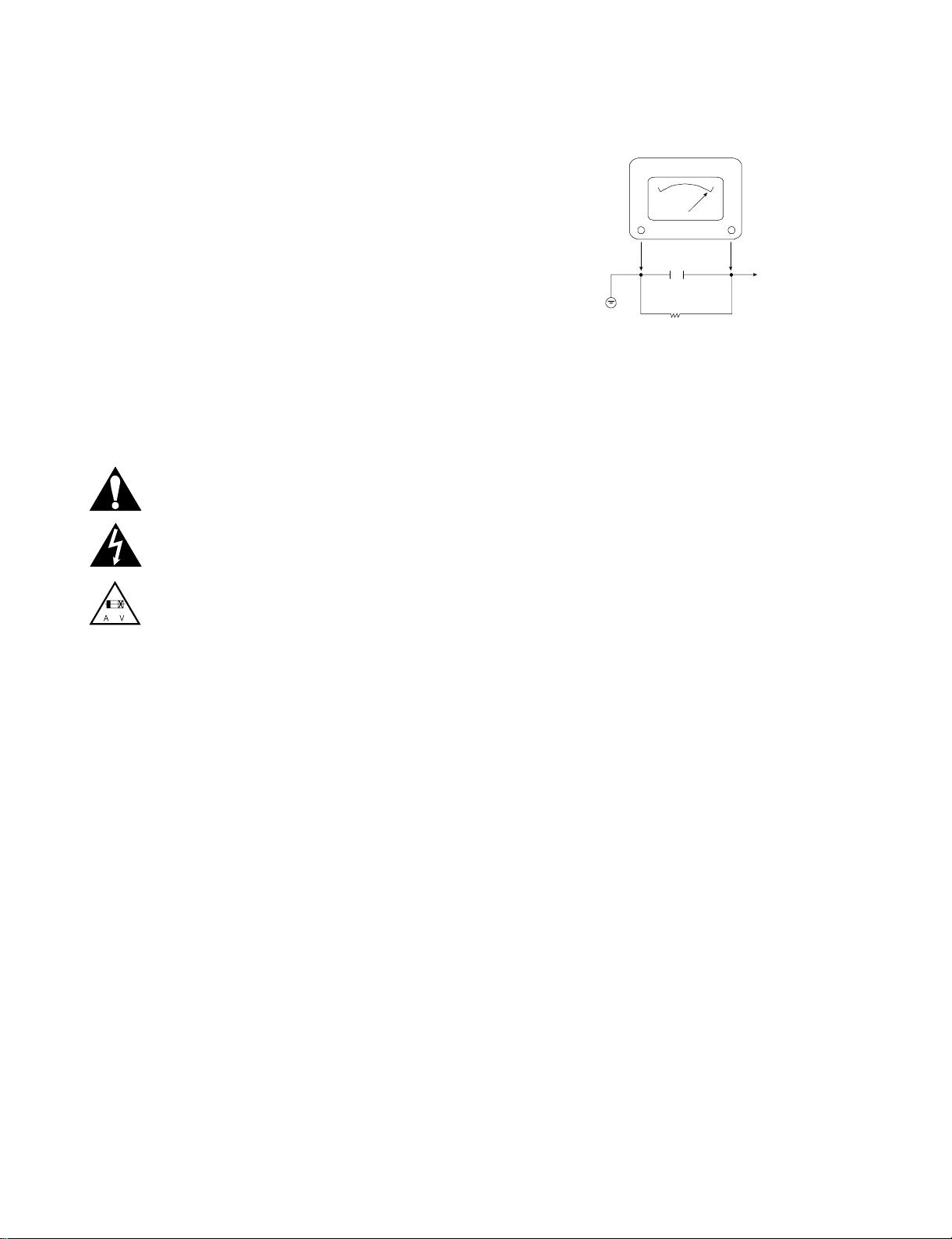
6. After reassembly of the set, always perform an AC leakage test on all
exposed metallic parts of the cabinet (the channel selector knobs, antenna
terminals, handle and screws) to be sure that set is safe to operate without
danger of electrical shock. DO NOT USE A LINE ISOLATION TRANSFORMER DURING THIS TEST. Use an AC voltmeter having 5000 ohms per
volt or more sensitivity in the following manner: Connect a 1500 ohm, 10
watt resistor, paralleled by a .15 mfd 150V AC type capacitor between a
known good earth ground water pipe, conduit, etc.) and the exposed metallic parts, one at a time. Measure the AC voltage across the combination of
1500 ohm resistor and .15 mfd capacitor. Reverse the AC plug by using a
non-polarized adaptor and repeat AC voltage measurements for each
exposed metallic part. Voltage measured must not exceed 0.75 volts RMS.
This corresponds to 0.5 milliamp AC. Any value exceeding this limit constitutes a potential shock hazard and must be corrected immediately.
TIPS ON PROPER INSTALLATION
1. Never install any receiver in a closed-in recess, cubbyhole, or closely fitting
shelf space over, or close to, a heat duct, or in the path of heated air flow.
2. Avoid conditions of high humidity such as: outdoor patio installations where
dew is a factor, near steam radiators where steam leakage is a factor, etc.
3. Avoid placement where draperies may obstruct venting. The customer
should also avoid the use of decorative scarves or other coverings that
might obstruct ventilation.
4. Wall- and shelf-mounted installations using a commercial mounting kit must
follow the factory-approved mounting instructions. A product mounted to a
shelf or platform must retain its original feet (or the equivalent thickness in
spacers) to provide adequate air flow across the bottom. Bolts or screws
used for fasteners must not touch any parts or wiring. Perform leakage tests
on customized installations.
5. Caution customers against mounting a product on a sloping shelf or in a tilted position, unless the receiver is properly secured.
6. A product on a roll-about cart should be stable in its mounting to the cart.
Caution the customer on the hazards of trying to roll a cart with small casters across thresholds or deep pile carpets.
7. Caution customers against using extension cords. Explain that a forest of
extensions, sprouting from a single outlet, can lead to disastrous consequences to home and family.
PRODUCT SAFETY SERVICING GUIDELINES FOR VIDEO PRODUCTS
A.C. Voltmeter
Good Earth Ground
such as the Water
Pipe, Conduit, etc.
0.15uF
1500 OHM
10 WATT
Place this probe
on each exposed
metal part.
Page 4

1-3
SERVICING PRECAUTIONS
CAUTION: Before servicing the HD/SD PERSONAL VIDEO
RECORDER & RECEIVER WITH GEMSTAR covered by
this service data and its supplements and addends, read and
follow the
SAFETY PRECAUTIONS. NOTE: if unforeseen
circumstances create conflict between the following servicing precautions and any of the safety precautions in this publications, always follow the safety precautions.
Remember Safety First:
General Servicing Precautions
1. Always unplug the HD/SD PERSONAL VIDEO
RECORDER & RECEIVER WITH GEMSTAR AC power
cord from the AC power source before:
(1)Removing or reinstalling any component, circuit board,
module, or any other assembly.
(2) Disconnecting or reconnecting any internal electrical
plug or other electrical connection.
(3) Connecting a test substitute in parallel with an elec-
trolytic capacitor.
Caution: A wrong part substitution or incorrect
polarity installation of electrolytic capacitors may result
in an explosion hazard.
2. Do not spray chemicals on or near this HD/SD PERSON-
AL VIDEO RECORDER & RECEIVER WITH GEMSTAR
or any of its assemblies.
3. Unless specified otherwise in this service data, clean
electrical contacts by applying an appropriate contact
cleaning solution to the contacts with a pipe cleaner,
cotton-tipped swab, or comparable soft applicator.
Unless specified otherwise in this service data, lubrication
of contacts is not required.
4. Do not defeat any plug/socket B+ voltage interlocks with
which instruments covered by this service manual might
be equipped.
5. Do not apply AC power to this HD/SD PERSONALVIDEO
RECORDER & RECEIVER WITH GEMSTAR and / or any
of its electrical assemblies unless all solid-state device
heat sinks are correctly installed.
6. Always connect the test instrument ground lead to an
appropriate ground before connecting the test instrument
positive lead. Always remove the test instrument ground
lead last.
Insulation Checking Procedure
Disconnect the attachment plug from the AC outlet and turn
the power on. Connect an insulation resistance meter (500V)
to the blades of the attachment plug. The insulation resistance between each blade of the attachment plug and accessible conductive parts (Note 1) should be more than 1Mohm.
Note 1: Accessible Conductive Parts include Metal panels,
Input terminals, Earphone jacks,etc.
Electrostatically Sensitive (ES) Devices
Some semiconductor (solid state) devices can be damaged
easily by static electricity. Such components commonly are
called Electrostatically Sensitive (ES) Devices. Examples of
typical ES devices are integrated circuits and some field
effect transistors and semiconductor chip components.
The following techniques should be used to help reduce the
incidence of component damage caused by static electricity.
1. Immediately before handling any semiconductor component or semiconductor-equipped assembly, drain off any
electrostatic charge on your body by touching a known
earth ground. Alternatively, obtain and wear a commercially available discharging wrist strap device, which
should be removed for potential shock reasons prior to
applying power to the unit under test.
2. After removing an electrical assembly equipped with ES
devices, place the assembly on a conductive surface such
as aluminum foil, to prevent electrostatic charge buildup or
exposure of the assembly.
3. Use only a grounded-tip soldering iron to solder or unsolder
ES devices.
4. Use only an anti-static solder removal device. Some
solder removal devices not classified as “anti-static” can
generate electrical charges sufficient to damage ES
devices.
5. Do not use freon-propelled chemicals. These can
generate an electrical charge sufficient to damage ES
devices.
6. Do not remove a replacement ES device from its protective package until immediately before you are ready to
install it. (Most replacement ES devices are packaged with
leads electrically shorted together by conductive foam,
aluminum foil,or comparable conductive material).
7. Immediately before removing the protective material from
the leads of a replacement ES device, touch the protective
material to the chassis or circuit assembly into which the
device will be installed.
Caution: Be sure no power is applied to the chassis or
circuit, and observe all other safety precautions.
8. Minimize bodily motions when handling unpackaged
replacement ES devices. (Normally harmless motion such
as the brushing together of your clothes fabric or the lifting
of your foot from a carpeted floor can generate static electricity sufficient to damage an ES device.)
Page 5

1-4
INTRODUCTION
- MSDVR & DVD Recorder receives the analog NTSC or cable broadcasting and compresses the audio and
video file into the MPEG format to save on HDD or record on DVD.
It supports the additional service of EPG (Electronics Program Guide) provided from MS.
-
Configuration
For the CPU, Intel Celeron 733 of x86 is used and for peripheral chips, CPU I/F, Memory I/F and North
Bridge and system parts for the North Bridge part that supports PCI I/F, IDE I/F serial I/F and USB I/F for
graphics function are used.
The Audio/Video signal received from the tuner or external input is compressed through the MPEG Encoder
and saved on HDD to be decoded by the CPU for display and if needed, saved on DVD.
Download or upgrade the MS EPG software through Ethernet and MODEM.
The file can be shared with Windows XP PC through Ethernet or USB I/F WiFi device.
It can be connected to an external HDD, Memory Card Reader, Memory Stick or WiFi device through USB
I/F.
• System Part
- CPU : Celeron 733(Low Voltage)
- North Bridge : 830
- System Memory : SDRAM 128MByte
• MPEG-2 Encoder Part
- MPEG-2 Encoder : CX23418
- PCI I/F ,Video Decoder/ Audio Processor
• Interface Part
- South Bridge : ICH4
- IDE I/F: HDD, DVD±RW
- Super I/O
- Ethernet
- MODEM
- USB 2.0
• Audio/Video In/Out Part
- Tuner
- Video Out
- Audio CODEC
Page 6

1-5
SPECIFICATIONS
Television System NTSC, Analog American Standard (480i)
Channel Coverage Unscrambled Air/Analog CATV 1-135
Draft Specification
NTSC Reception 1. Terrestrial (ANT/Analog)
2. Cable (CABLE/Analog)
DVD±R/W
USB 2.0
Network 1. Ethernet(10/100)
2. Modem(56kbps)
HDD(160GB)
DVD ± R/W Specifications
DVD DVD-ROM : 4.7GB (Single Layer)
8.5GB (Dual Layer)
DVD-R : 4.7GB (Ver. 2.0 for Authoring : R & W)
4.7GB (Ver. 2.0 for General: read & write )
DVD-RW : 4.7GB (Ver. 1.1 read & write)
DVD+R : 4.7GB/side (Ver. 1.1 read & write)
DVD+RW : 4.7GB/side (Ver. 2.1 read & write)
CD CD-ROM Mode-1 data disc
CD-ROM Mode-2 data disc
CD-ROM XA, CD-I, Photo-CD Multi-Session, Video CD
CD-Audio Disc
Mixed mode CD-ROM disc (data and audio)
CD-Extra, CD-Text
CD-R (Conforming to “Orange Book Part 2”: read)
CD-RW (Conforming to “Orange Book Part 3”: read)
Inputs/Output
RF Input Air/Cable TV (1)
RF Output Out To TV (1) (Loop Out)
Component Video Output Component Out (1), RCA Jack connector 480p,480i -> YPbPr
S-Video Output simultaneous Out with CVBS
S-Video Out (1), 4-pin Mini-DIN
Composite Video Output Video Out, RCA Jack connector (1-Port)
Simultaneous Out with S-video
Video Output Selection Switch 480i -> Composite
480i,480p -> Component Selection
Video In 480i Composite NTSC
Video In with L/R in(2), RCA Jack connector
S-Video In S-Video In, 4-pin Mini-DIN
Audio out L/R Out(2),SPDIF Out(1: Optical, 1: Coaxial)
USB USB2.0(2-Port)
Ethernet 10BASE-T/100BASE-T, RJ45(1)
Modem 56kbps Data Modem, RJ11(1)
VCR/Cable Box Control IR Expender(1), Phone Jack Serial(1)
Chassis Size 430mm(W) x 300mm(D) x 59mm(H)
Page 7

1-6
* DVR – Recording & Scheduling
• Instant recording / Series recording / Manual recording
• Conflict management
• Duplicate checking (recognize and ignore reruns and repeats)
* DVR - Live TV
• 90 minutes buffer
• Recording Pause buffer
• Buffers live TV while playing a recorded TV program
* DVR - Playback
• Skip ahead : 30 seconds
• Instant Replay : 7 seconds
• Multi speed FF & RW : 3 speed (3x,40x,250x)
• Slow motion : FWD 1/2x
• Frame advance
* DVR – etc.
• DVR functionality can work while DVD burning in progress
• Arrange recorded shows into folders
* Program Guide & Search
• Guide data : 14 days premium service
• Guide date source : dialup or broadband
• Combines channel guides from multiple sources
• Channel filtering
• Search by Title, Category, Topic (keyword)
* DVD - Recording
• Disc Compatibility
DVD-R/DVD-RW, DVD+R/DVD+RW, Double layer
Not support VR mode recording
• DVD burning speed : x4
• Copy programs to DVD
• Create the DVD top menu and program info submenu
• Auto chapter marking : every 10 minutes
• Record shows to DVR while burning a DVD
• Use the box’s other functions during burning process
* DVD - Playback
• Disc Compatibility
DVD-Video, DVD-R/DVD-RW, DVD+R/DVD+RW
DVD-/+RW
Audio CD, CD-R, CD-RW
• Play a DVD or CD
• Angle/Subtitle selection, change audio language
• DVD playback while recording/buffering
* Photo & Music
• Digital photo slideshow
• Play music
• Photo slideshows while playing music
* Networking
• Fetch guide data over broadband
• 802.11 a/g wireless USB adaptor support
Vender and model name ?
* Other Features
• Video On Demand(V1.1)
• Software update
• USB memory card reader support
Page 8

1-7
SYSTEM S/W UPGRADE
1. ON-LINE S/W UPGRADE METHOD
- The software can be upgraded by connecting with Ethernet or MODEM.
Main Menu -> settings -> guide set-up -> ???
The softwares that can be upgraded online are as follows.
- Main S/W
- Bootloader
- DVD Firmware
2. SYSTEM INFORMATION
In this menu, you can check the version, Box ID and basic system information of all the softwares used in the
system.
You can check this information in Main menu-> Settings -> System Information.
The information that can be checked is as follows.
- Main S/W version
- Bootloader version
- DVD Firmware version
The information that can be checked.
- Service ID
- Network Information
- Uptime: Power up time
- BR: Bit rate indication
- CPU temperature
Page 9
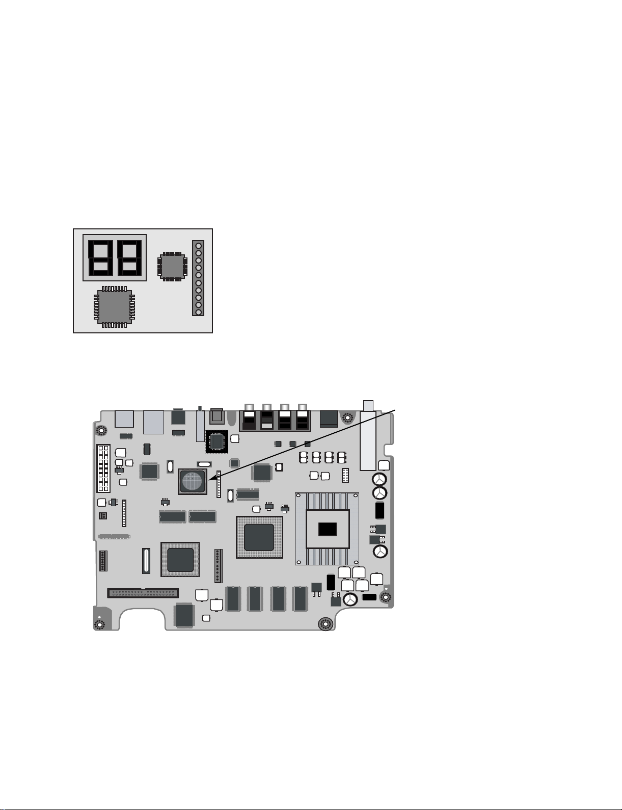
1. TEST METHOD USING THE DEBUG BOARD
There are two test methods when there is an issue with the main board.
When it is not properly booted and the composite video is not displayed, you can check the status of the board
using the Debug Board for debugging prepared in the Debug port of the main board.
The Debug Board is composed as follows.
- 7-Segment that indicates the board status
- The connector interfacing the Debug port
- Boot ROM for testing: Not used.
How to use the Debug Board
The Debug Board is connected to the J802 of the main board.
Error code indicated on the Debug Board
1-8
TEST S/W
Eth
G-
MO
K4 K4K4 K4
ern
RT
L81
Si
CX2
2
8
A
FS4
54
Au
Au
Co
P
Au
AuViAu
Vi
S
S
830
Cele
S6 S6S6 S6
J802
Page 10

1-9
During L2 cache initialization, the processor is running at a faster or
slower bus frequency than it is designed for. This is a fatal error, and
the processor will be halted. Detected during cache initialization.
No memory was detected during the memory initialization. This is a
fatal error, and the processor will be halted.
Unsupported memory was detected during the memory initialization.
This is a fatal error, and the processor will be halted.
An invalid timing configuration was detected (e.g. 66 MHz SDRAM
with a 100 MHz host bus frequency).
Both registered and unregistered DIMMs were detected.
An unsupported memory configuration was detected.
The stack was located above 1 Mbyte when attempting to switch to
real mode by a call to the sflDone16 API.
The detected amount of memory does not match the SPD data.
Unsupported The host bus frequency is not supported.
The requested integrity mode is not supported by the Hardware.
Board initialization(SIO, GPIO(A/V Mute) etc.)
Prepare to handle interrupts
initialize caching and shadow ROM to RAM
Super I/O initialization
Initialize local keyboard if present
initialize A TA
chipset pci resource allocation
board specific resource allocation hook
enable memory and i/o address decoding for pci devices
Standard legacy services setup
initialize memory map
Setup the graphics mode for 830M
System Bus Frequency
Mismatch
No Memory Detected
Unsupported Memory Type
Unsupported Timing
Mixed Registered/ Unregistered
DIMMs
Unsupported Memory
Configuration
Invalid Real Mode Stack
SPD and Memory Mismatch
Host Bus Frequency
Integrity Mode Unsupported
board init
interrupt init
Cache init
SIO init
keyboard init
ATAinit
csPciAlloc
boardResourceAlloc
pciEnableDecode
lgcyInitSvcs
mmapinit
board video init
0x30
0x31
0x32
0x33
0x34
0x35
0x36
0x37
0x38
0x3A
0x20
0x21
0x22
0x23
0x25
0x26
0x27
0x28
0x29
0x2A
0x22
0x2F
BOOTLOADER ERROR/STATUS CODE
Code Name Interpretation/Description
Page 11
1-10
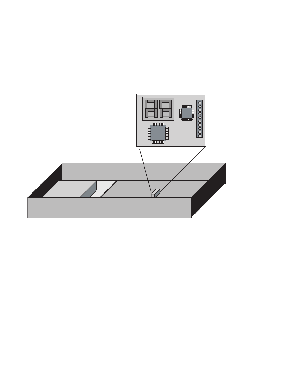
2. BOARD TEST METHOD USING THE JIG SET
Diagram of JIG test composition
For the JIG set, use the RV7922M set excluding the main board and HDD.
When using the set for JIG, you must use the Debug Board. You must use the HDD for JIG.
Because of the software protection policy of MS, the service man cannot include the self diagnosis software
for troubleshooting on the mass produced HDD. Therefore Boot ROM and HDD are separately needed to
repair the board.
The MS software policy is configured to only allow the Signed Image to be operated on the Signed Boot ROM.
D
VD Loader
Power
Main Board
HDD
Page 12

2-1
SECTION 2
CABINET & MAIN CHASSIS
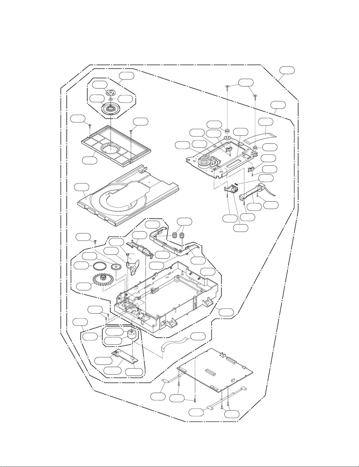
CONTENTS
EXPLODED VIEWS.....................................................................................................................2-2
1. Cabinet and Main Frame Section...........................................................................................2-2
2. Deck Mechanism Section(RL-05)...........................................................................................2-3
Page 13
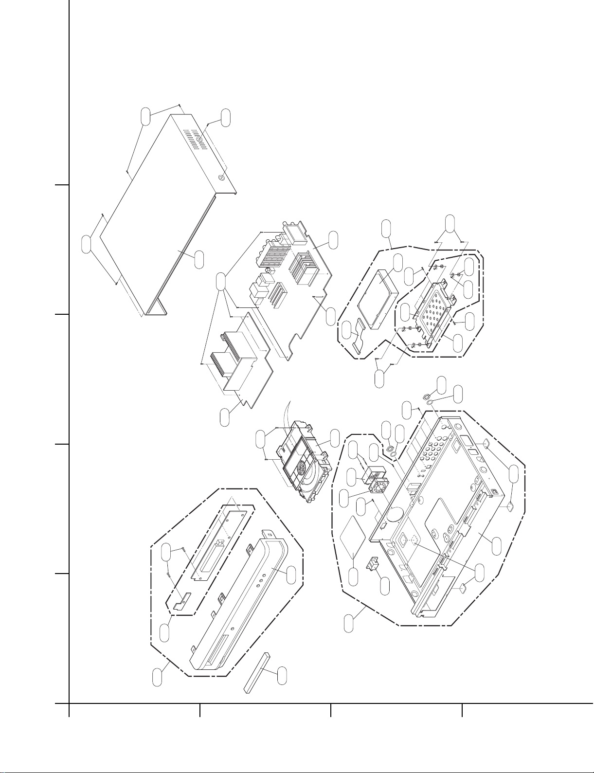
2-2
EXPLODED VIEWS
1. CABINET AND MAIN FRAME SECTION
A
4
3
2
1
BCD
463
463
250
462
463
A47
463
A46
462
A60
205
469
457
473
A26
472
204
471
473
203
474
202
201
474
A26A
472
471
465
263
264
A44
266
457
261
267
452
280
A43
A50
283
261
260
Page 14
2-3
2. DECK MECHANISM SECTION(RL-05)
1434
1026
1435
1015
1003
1005
1016
1001
1013
1014
A001
1002
1434
1012
1019
1011
1009
1038
1024
1432
1029
1019
1025
1027
1020
1433
1437
1029
1432
1033
1021
A60
A000
1030
1025
1027
1432
1032
1432
1017
A004
1436
1018
1018A
1018B
1018C
1018E
1018D
1042
1434
1006
1041
A002
1434
Page 15

3-1
SECTION 3
ELECTRICAL
CONTENTS
ELECTRICAL TROUBLESHOOTING GUIDE ..................................................................................................3-2
1. POWER(SMPS) CIRCUIT ........................................................................................................................3-2
2. SYSTEM PART CIRCUIT .........................................................................................................................3-3
3. VIDEO PART-1..........................................................................................................................................3-5
4. YPBPR VIDEO OUTPUT TROUBLESHOOTING.....................................................................................3-6
5. S-VIDEO VIDEO OUTPUT TROUBLESHOOTING..................................................................................3-7
6. CVBS VIDEO OUTPUT TROUBLESHOOTING.......................................................................................3-8
7. AUDIO TROUBLESHOOTING..................................................................................................................3-9
8. TUNER TROUBLESHOOTING...............................................................................................................3-10
9. ETHERNET TROUBLESHOOTING........................................................................................................3-11
10. MODEM TROUBLESHOOTING...........................................................................................................3-12
11. DVD TROUBLESHOOTING..................................................................................................................3-13
12. IR BLASTER TROUBLESHOOTING ....................................................................................................3-14
13. SERIAL (RS-232) TROUBLESHOOTING.............................................................................................3-15
WAVEFORMS ..................................................................................................................................................3-16
1. SYSTEM PART-1 ....................................................................................................................................3-16
2. SYSTEM PART-2 ....................................................................................................................................3-17
3. VIDEO PART-1........................................................................................................................................3-18
4. VIDEO PART-2........................................................................................................................................3-19
5. VIDEO PART-3........................................................................................................................................3-20
6. VIDEO PART-4........................................................................................................................................3-21
7. AUDIO PART -1........................................................................................................................................3-22
8. AUDIO PART -2........................................................................................................................................3-23
9. AUDIO PART -3........................................................................................................................................3-24
10. ETHERNET PART ............................................................................................................... .................3-25
11. SUPER IO & FRONT INTERFACE PART.............................................................................................3-26
BLOCK DIAGRAMS........................................................................................................................................3-27
1. TOTAL BLOCK DIAGRAM......................................................................................................................3-27
2. WRING BLOCK DIAGRAM.....................................................................................................................3-28
3. POWER BLOCK DIAGRAM ...................................................................................................................3-29
4. SIGNAL PATH BLOCK DIAGRAM..........................................................................................................3-30
5. BLOCK DIAGRAM..................................................................................................................................3-31
CIRCUIT DIAGRAMS......................................................................................................................................3-32
1. POWER(SMPS) CIRCUIT DIAGRAM ....................................................................................................3-32
2. POWER CIRCUIT DIAGRAM.................................................................................................................3-34
3. CPU CIRCUIT DIAGRAM.......................................................................................................................3-36
4. GMCH CIRCUIT DIAGRAM ....................................................................................................................3-38
5. ICH4 CIRCUIT DIAGRAM ......................................................................................................................3-41
6. CLOCK & LPC CIRCUIT DIAGRAM .......................................................................................................3-42
7. MEMORY/IDE CIRCUIT DIAGRAM........................................................................................................3-44
8. LAN/USB/MODEM CIRCUIT DIAGRAM ................................................................................................3-46
9. VIDEO CONVERTER & AC97 CODEC CIRCUIT DIAGRAM ................................................................3-48
10. MPEG-II ENCODER & AV DECODER (CX23418) CIRCUIT DIAGRAM.............................................3-50
11. TUNER & EXTERNALAV INPUT CIRCUIT DIAGRAM........................................................................3-52
12. AUDIO/VIDEO INPUT INTERFACE CIRCUIT DIAGRAM ....................................................................3-54
13. MISCELLANEDUS CIRCUIT DIAGRAM ..............................................................................................3-56
14. EXTERNAL I/F CIRCUIT DIAGRAM ....................................................................................................3-58
PRINTED CIRCUIT DIAGRAMS.....................................................................................................................3-60
1. MAIN PRINTED CIRCUIT DIAGRAMS(TOP VIEW) ..............................................................................3-60
2. MAIN PRINTED CIRCUIT DIAGRAMS(BOTTOM VIEW) ......................................................................3-62
3. KEY PRINTED CIRCUIT DIAGRAM.......................................................................................................3-64
4. TIMER PRINTED CIRCUIT DIAGRAM...................................................................................................3-64
5. POWER PRINTED CIRCUIT DIAGRAM ................................................................................................3-66
Page 16
3-2
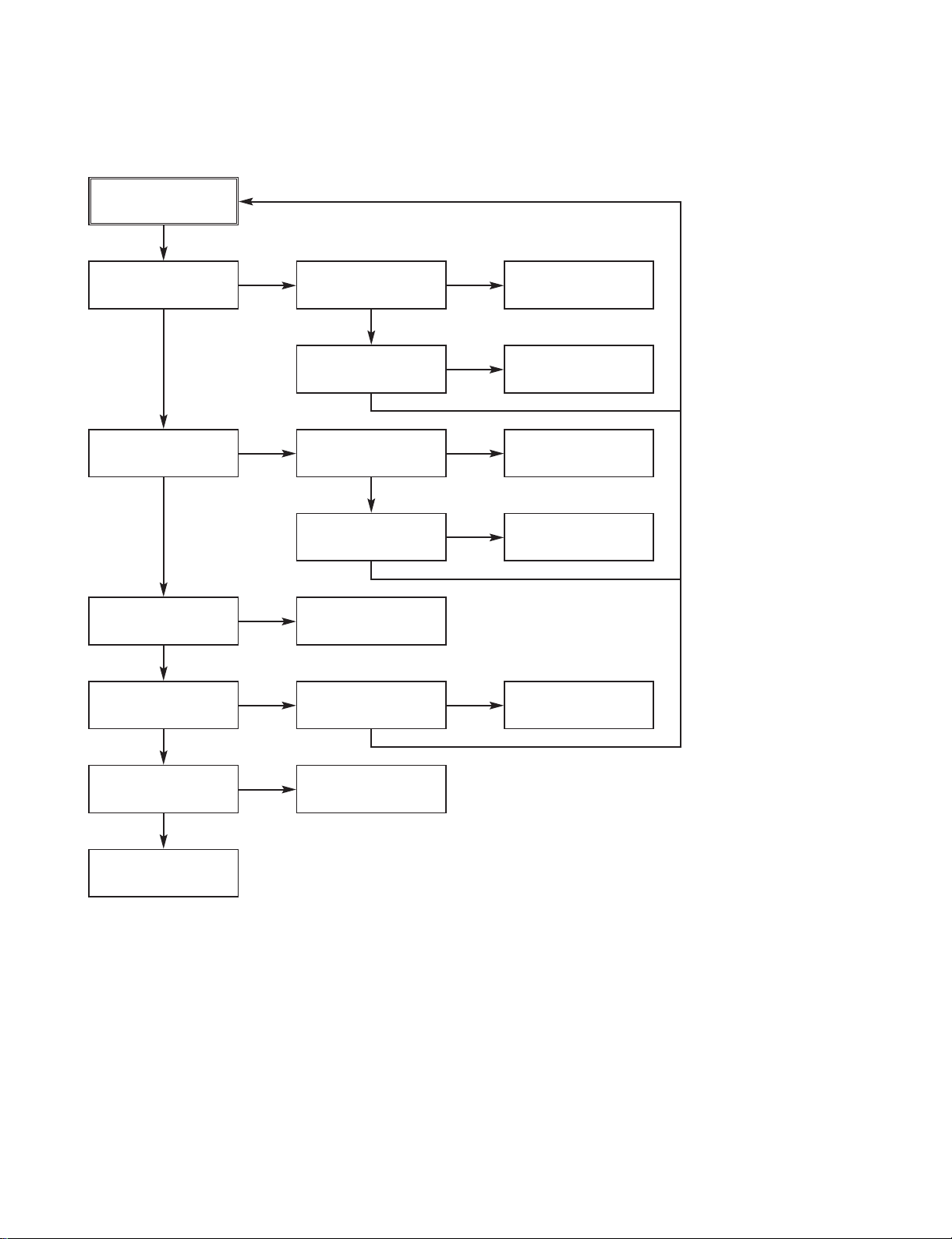
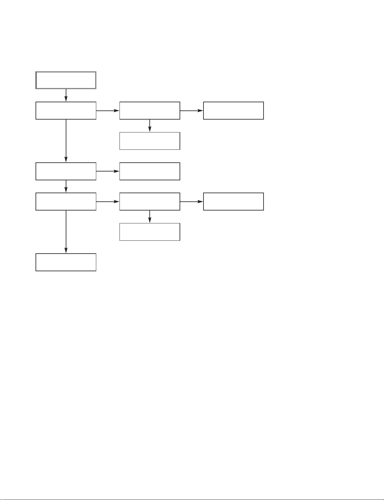
ELECTRICAL TROUBLESHOOTING GUIDE
NO
Proper display port
select
Video Input Cable
connection OK
1. POWER(SMPS) CIRCUIT
Power cable
connection
Front Signal Cable
Connection OK
“HELLO” display
on VFD OK
“LG logo” display
on Monitor OK
NO
Front signal cable
connect
NO
NO
NO
NO
NO
Front Power Cable
Connection OK
NO
Front power cable
connect
Display Cable
Connection OK
NO
Display Cable
Connect
Display Port
Selection (S800) OK
HDD Image
upgrade
Audio Cable
Connection OK
NO
Audio Cable
Connect
YES
YES
YES
YES
YES
YESYES
YES
YES
YES
“CH No. & DATE”
display on VFD OK
Audio OK
Video OK
Normal TV
Function OK
Page 17
3-3
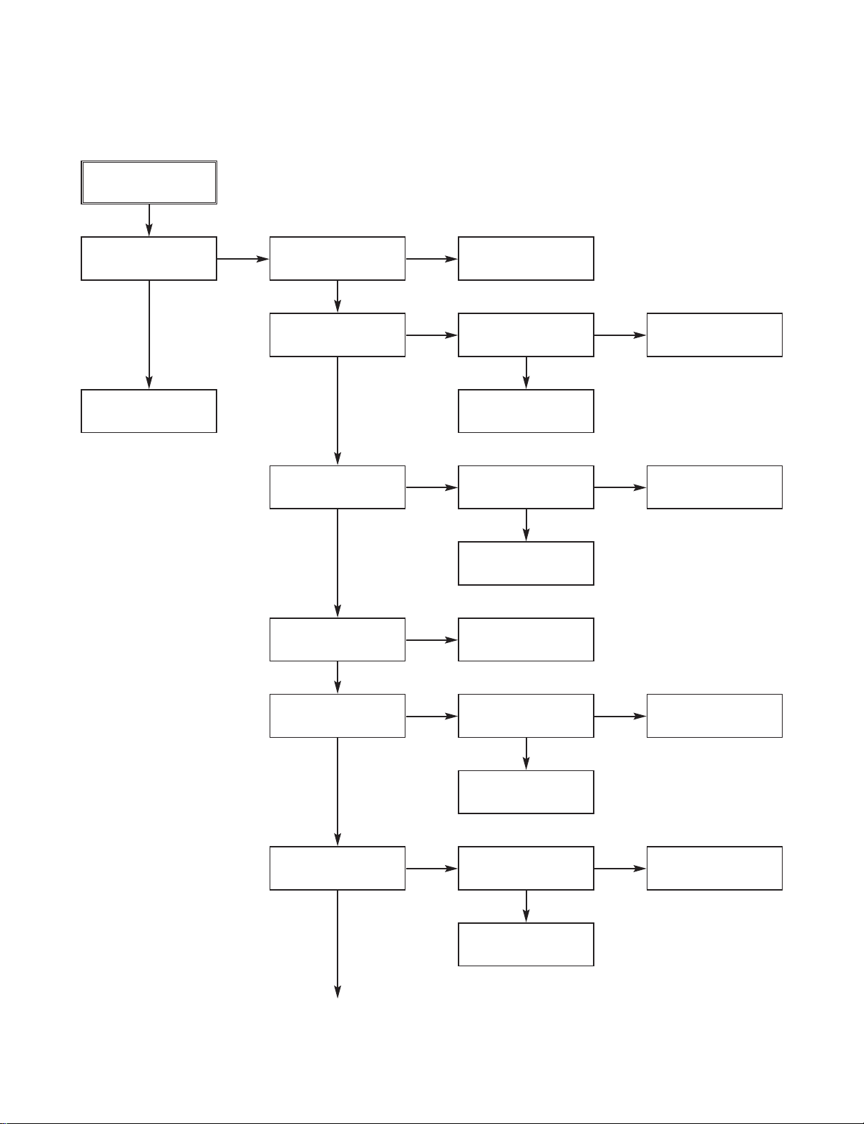
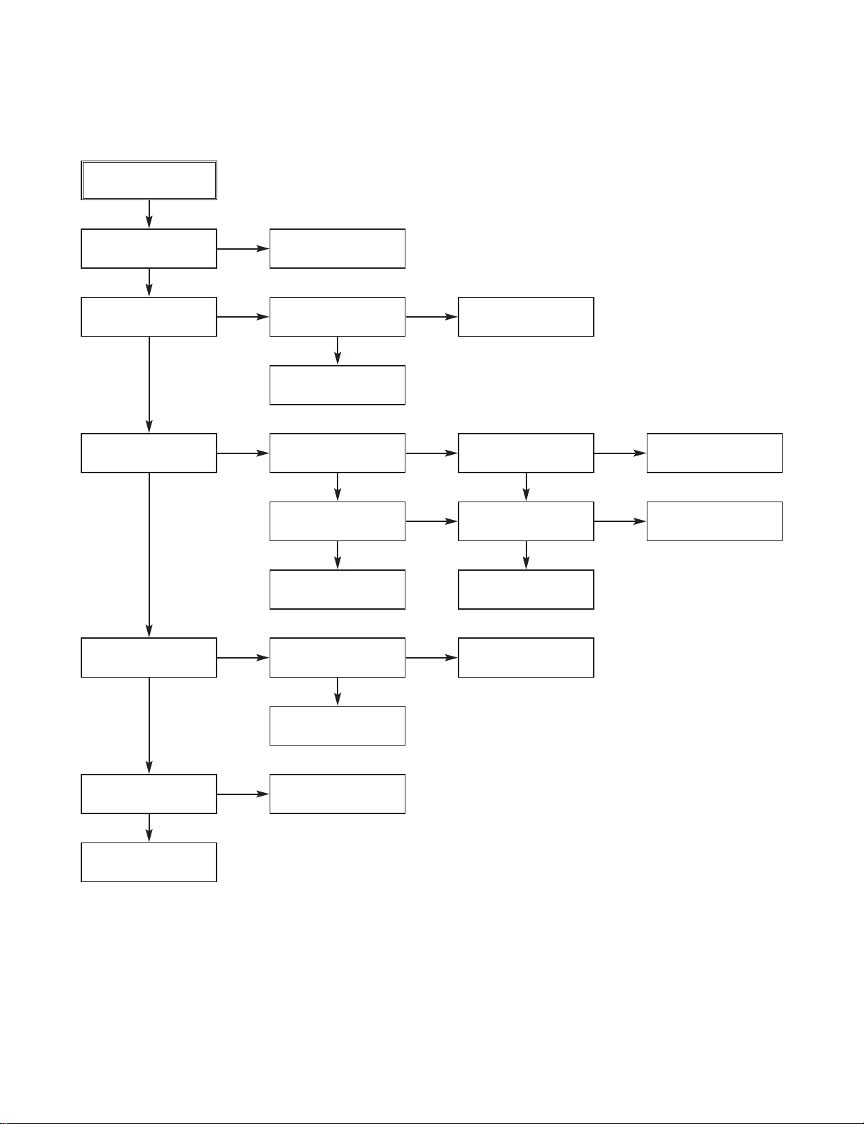
2. SYSTEM PART CIRCUIT
Power Cable
Connection Power on
LED801 “ON” OK
“LG logo” display
on Monitor OK
system function
OK
NO
Check soldering
state of Board
NO
C919 +1.25V OK
IC900 change
NO
IC900 (1-Pin) +12V
OK
NO
NO
Q909 (2-Pin)
Low=0V OK
IC902 change
X100 change
NO
NO
X300 14.318MHz
OK
IC301 change
IC301 (24-Pin)
66MHz OK
IC301 change
NO
J900 Connector
Power Cable Check
NO
IC914 change
YES
YES
YES
YES
YES
C930 +1.15V OK
X100 32.768KHz
OK
IC301(49-pin)
133MHz OK
YES
YES
YES
IC301(10-pin)
33MHz OK
YES
YES
YES
YES
NO
NO
X300 change
R179,C210
Resoldeing
Page 18
3-4
IC302(74-pin)
High=+3.3V OK
IC300(24-pin)
High=+3.3V OK
IC302(63-pin)
High=+3.3V OK
NO
Check IC104
R326 Re-soldering
NO
NO
NO
HDD Cables
Re-connection
R377, J302
Re-soldering
NO
IC302 change
HDD Cables
Connection OK
IC302(64-pin)
High=+3.3V OK
Change HDD
YESYES
YES
YES
YES
YES
Page 19
3-5
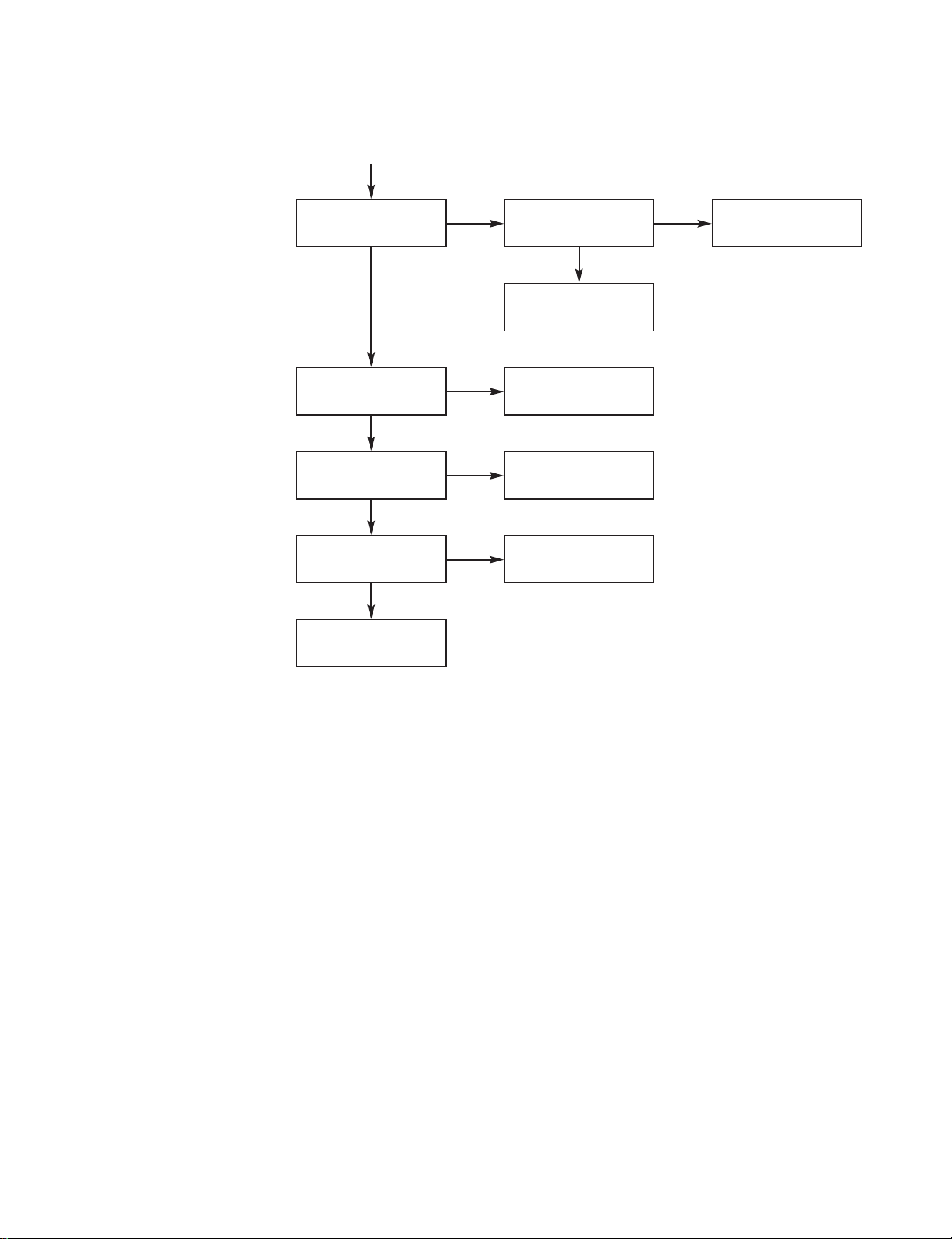
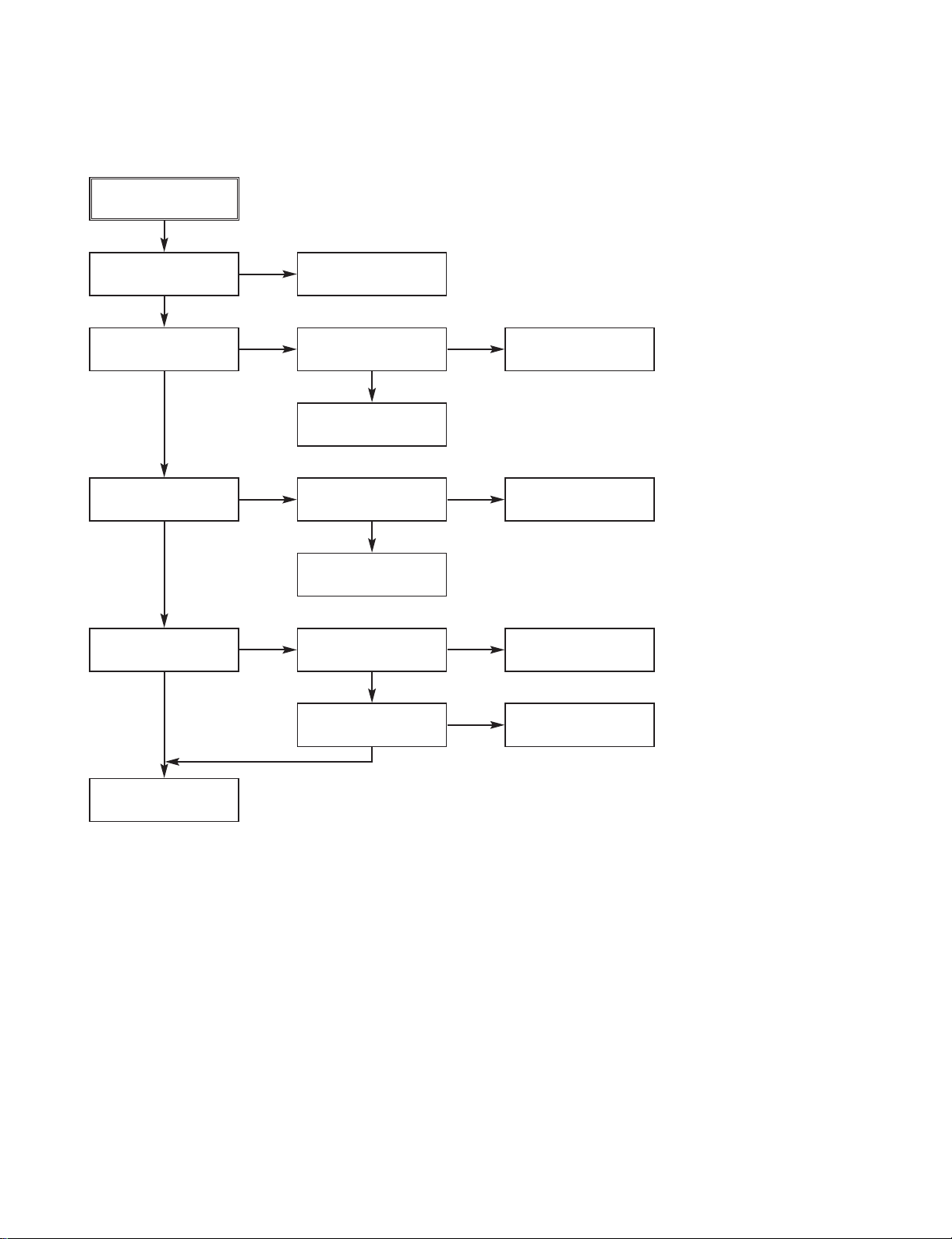
3. VIDEO PART-1
No display
IC302(73-pin)
‘3.3V’=high OK
IC501(53-pin)
‘3.3V’= high OK
IC501(63-pin)
27MHz clock in OK
IC501(51,54-pin)
Clock in OK
NO
NO
NO
IC302 change
NO
OSC500 change
NO
Re-soldering
NO
R373 Re-soldering
YES
YES
YES
YES
YES
YES
YES
YES
OSC500(3-pin)
27MHz clock out OK
YES
YES
R508 Re-soldering
IC103 check
IC501(44,45-pin)
I2C BUS OK
NO
IC501(56-pin)
Clock out OK
NO
Q504,Q505, R532 ~
R535 soldering OK
IC103 check
IC501 change
R521 ~ R524, L500
~ L503 Soldering OK
NO
Re-soldering
C544 ~ C547,C560 ~
C563 Soldering OK
NO
Re-soldering
Video Part OK
YES
Page 20
3-6
4. YPBPR VIDEO OUTPUT TROUBLESHOOTING
No display
Cable connect
Video Cable
connection OK
S800 status OK
IC510(3,5-pin) Video
signal input OK
IC509,510 (8-pin)
+5V OK
NO
NO
NO
NO
S800 setting 480i
or 480p
NO
Video Part-1 check
NO
Q815, R881 ~ 883,
R839 Check
Re-soldering
NO
YES
YES
YES
YES
YES
YES
YES
YES
YES
YES
YES
IC509(3-pin) Video
signal input OK
IC803 (4-pin)
Under +2.5V OK
IC803 Check
IC509,510 (4-pin)
-5V OK
IC509(1-pin) IC510(1,7-pin)
Video signal output OK
R774, R775, FL510,
FL512 Soldering OK
YPbPr
Video Output OK
NO
NONO
NO
J900 (3-pin) check
R740, R742, R745, R746, R762,
R765, R758 ,R759 soldering OK
IC510 Check
R738, R741,R743,
R744 soldering OK
NO
Re-soldering
IC509 Check
Re-soldering
Video Part-1 check
Page 21

3-7
5. S-VIDEO VIDEO OUTPUT TROUBLESHOOTING
No display
Cable connect
Video Cable
connection OK
NO
YES
YES
S800 setting CVBS
S800 status OK
NO
YES
Video Part-1 check
IC508(3,5-pin) Video
signal input OK
NO
YES
IC803 (4-pin)
Under +2.5V OK
IC803 Check
J900 (3-pin) check
R731, R732, R733,
R734 soldering OK
IC508 Check
R735, R736, R737, R739
C652, soldering OK
IC508 Check
Re-soldering
IC508 (8-pin) +5V
OK
IC508 (4-pin) -5V
OK
IC508(1,7-pin) Video
signal output OK
R774, R775, FL510,
FL512 Soldering OK
S-Video Video
Output OK
NO
NO
NO
NO
Q815, R881~883,
R839 Check
Re-soldering
Re-soldering
NO
NO
NO
YES
YES
YES
YES
YES
YES
YES
Page 22
3-8
6. CVBS VIDEO OUTPUT TROUBLESHOOTING
No display
Cable connect
Video Cable
connection OK
NO
YES
YES
S800 setting CVBS
or 480i
S800 status OK
NO
YES
Video Part-1 check
IC509(5-pin) Video
signal input OK
NO
YES
IC803 (4-pin)
Under +2.5V OK
IC803 Check
J900 (3-pin) check
R756, R757, R761,
R764 soldering OK
IC509 Check
Re-soldering
IC509 (8-pin) +5V
OK
IC509 (4-pin) -5V
OK
IC509(7-pin) Video
signal output OK
R780,FL516
Soldering OK
CVBS
Video Output OK
NO
NO
NO
NO
Q815, R881~883,
R839 Check
Re-soldering
NO
NO
YES
YES
YES
YES
YES
YES
YES
Page 23
3-9
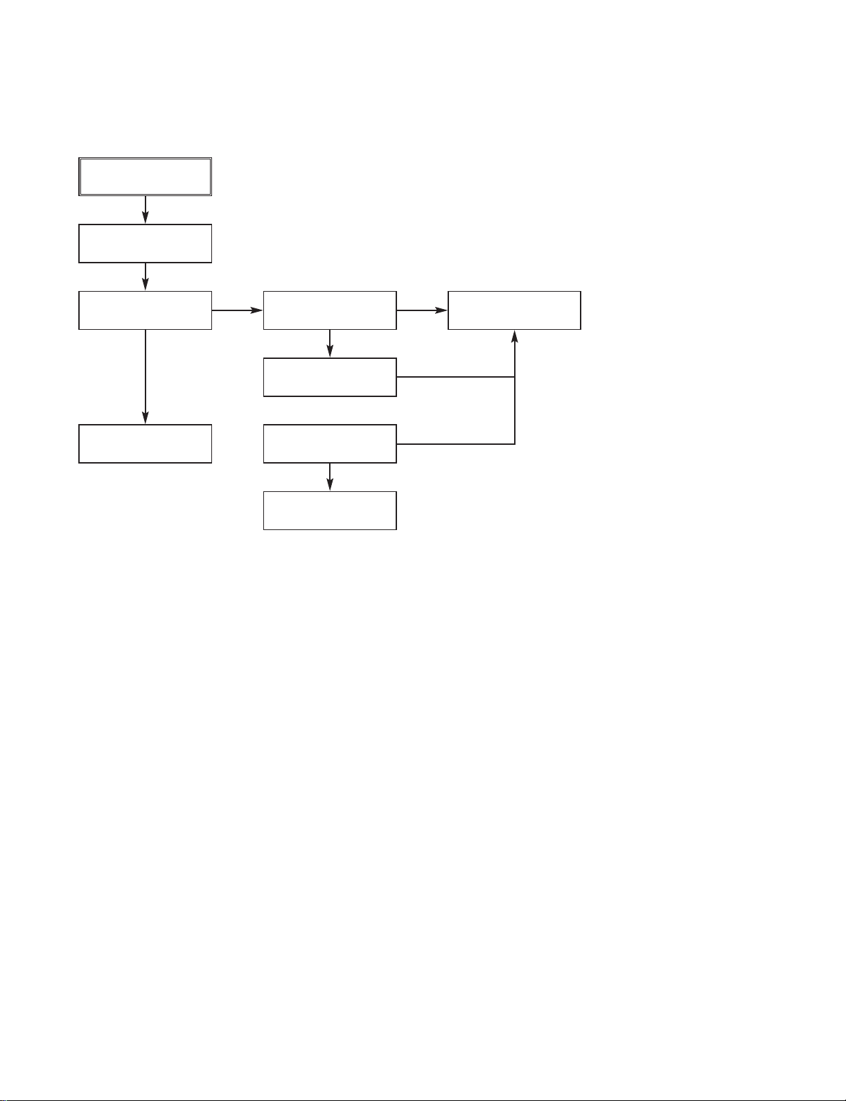
7. AUDIO TROUBLESHOOTING
Audio output
problem
IC104 Soldering
Check
IC500 (11-pin)
High = “1” OK
NO
YES
YES
System part check
IC500 (5, 6, 10-pin) Clock
/ Data / Sync Input Check
NO
YES
YES
IC500 (1, 9-pin)
+3.3V out OK
IC500 (2, 3-pin) 24.576MHz
clock In/Out OK
NO
YES
IC500 (25, 38-pin)
+5.0V out Check
IC500 soldering
Check
IC502 (8-pin) +8.0V
input OK
R528, R529 C554,
C555 Soldering OK
F509, F511, F517,
F518 Soldering OK
Audio Output OK
IC502 (1, 7-pin)
Audio out OK
NO
B504 soldering OK
Re-soldering
NO
J900 Connector
Power Cable Check
NO
B506 Soldering
Check
NO
NO
Re-soldering
NO
YES
YES
J900 Connector
Power Cable Check
YES
YES
YES
YES
Re-soldering
NO
Page 24
3-10
8. TUNER TROUBLESHOOTING
Tuner problem
IC803 (4-pin)
Under +2.5V OK
TU500(2,6-pin)
+5V Input OK
NO
Q815, R881~883,
R839 Check
NO
YES
YES
YES
IC803 Check
J900 (2-pin) Check
TU500(8-pin) +30V
Input OK
NO
YES
R651,652,724,
725 Soldering Ok
IC513 Check
J900 (2-pin) Check
Tuner OK
NO
R651, 652, 724,
725 Re-soldering
NO
YES YES
Page 25
3-11
9. ETHERNET TROUBLESHOOTING
Ethernet problem
Network Cable
Connect
Network Cable
Connection OK
NO
YES
YES
MAC Address
Check OK
Network Setup
Check OK
NO
NO
NO
NO
Forwarding Factory
NO
YES
YES
YES
YES
YES
Network Re-Setup
IC308 (60, 61-pin) 25
MHz Clock In/Out OK
IC905 (2, 4-pin)
+3.3V out OK
IC308 (51, 96-pin)
+2.5V out OK
IC308 soldering
Check
IC310 (8-pin) +3.3V
input OK
IC310 Change
IC310 Re-soldering
Or Change
IC310 (1,2,3,4-pin)
Clock/DataOK
IC310 (67, 68, 71,
72-pin) Output OK
Ethernet OK
IC905 (3-pin)
+5.0V out OK
J900 Connector
Power Cable Check
NO
NO
NO
YES
YES
YES
Q304 soldering OK
J900 Connector
Power Cable Check
YES
YES
YES
J900 Connector
Power Cable Check
NO
Re-soldering
NO
Page 26

3-12
10. MODEM TROUBLESHOOTING
No Dial-up
connection
Connection Phone
line
YES
YES
YES
YES
IC905 Check
IC307 (5,21-pin)
+3.3V input OK
J304(between 3,and
4 Pin) 40~52V OK
NO
Phone Line Check
NO
NO
NO
YES
YES
YES
IC304 (3-pin) Clock
Out 2048KHz OK
DTE Setup & Connection (8-bit, no
parity bit, one stop bit and 19.2kbps)
IC304 (1-pin) Clock
Input 27MHz OK
Re-soldering IC304
Check IC309 Refer
to Fig 7-10 OK
Change IC309
“AT” Response OK
Modem OK
Check OSC500
Re-soldering IC309
NO
NO
YES
YES
~
~
< Fig 7-10. IC309 Typical Voltage >
0V
0V
0V
0V
0.8V
0.7V
2.3V
1.0V
-- QE
-- DCT
-- RX
-- IB
-- C1B
-- C2B
-- VREG
-- RNG1
ON-HOOK
VREG2 --
DCT2 --
IGND --
DCT3 --
QB --
QE2 --
SC --
RNG2 --
0V
0V
0V
0V
0V
0V
~1.0V
1.6V
3.4V
2.5V
0V
0.8V
0.8V
2.3V
1.0V
OFF-HOOK
-- QE
-- DCT
-- RX
-- IB
-- C1B
-- C2B
-- VREG
-- RNG1
DCT2 --
IGND --
DCT3 --
QB --
QE2 --
SC --
VREG2 --
RNG2 --
2.2V
0V
1.6V
2.8V
2.1V
0V
1.8V
0.9V
Page 27
3-13
11. DVD TROUBLESHOOTING
DVD problem
DVD Loader
Power-On OK
YES
YES
YES YES
Front Panel Open/
Close Key Check OK
DVD Tray Open/
Close Check OK
NO
Front Panel Check
NO
J902 Connector
Power Cable Check
NO
J303 Connector
FFC Cable Check
NO
NO
YES
YES
DVD Auto-Loading
OK
DVD Region Code
Check OK
DVD Problem
DVD Video Check
OK
DVD Audio Check
OK
DVD Play Check
OK
DVD OK
DVD Disc Check
Video part Check
NO
NO
Audio part Check
NO
YES
YES
YES
Page 28
3-14
12. IR BLASTER TROUBLESHOOTING
IR Blaster Problem
Setting IR Blaster
Configuration
YES
YES
YES YES YES
J804(2-pin) “FLD_
CLK” Present OK
R859 IR Signal
Present OK
NO
Check IC302 &
Re-soldering
NO
NO
J804(4-pin) “FLD_
RXD” Present OK
IR Blaster
Operation OK
J804(3-pin) “FLD_
TXD” Present OK
Change
Front-Board
NO
YES
Page 29
3-15
13. SERIAL (RS-232) TROUBLESHOOTING
Serial (RS-232)
Problem
Serial Cable
Connection OK
YES
YES
J900 Connector
Power Cable Check
IC805(16-pin) +5V
Input OK
NO
YES
Check IC302 &
Re-soldering
J805(11-pin) “TX
Data” Present OK
NO
YES
YES
Check IC805 &
Re-soldering
B805 Re-soldering
J805(14-pin) “TX
Data” Present OK
NO
J805(13-pin) “RX”
Present OK
YES
J805(12-pin) “RX
Data” Present OK
YES
Serial (RS-232) OK
NO
NO
Serial Cable
Connect
NO
Page 30

3-16
WAVEFORMS
1. SYSTEM PART-1
Page 31

3-17
2. SYSTEM PART-2
Page 32

3-18
3. VIDEO PART-1
Page 33

3-19
4. VIDEO PART-2
Page 34

3-20
5. VIDEO PART-3
Page 35

3-21
6. VIDEO PART-4
Page 36

3-22
AI_DATA
AI_CLK AI_LRCLK
7. AUDIO PART-1
Page 37

3-23
AUD_LINK_BCLK
AUD_LINK_SDIN
AUD_LINK_SYNC
AUD_LINK_RST
8. AUDIO PART-2
Page 38

SPDIF
3-24
AUDIO_L
9. AUDIO PART-3
Page 39

3-25
TXD+
TXD-
RXIN+ RXIN-
25MHZ
10. ETHERNET PART
Page 40

3-26
FLD_RXD
FLD_CLK CLK_LPC_33MHZ
11. SUPER IO & FRONT INTERFACE PART
Page 41

3-27
1. TOTAL BLOCK DIAGRAM
BLOCK DIAGRAMS
SIF
Tuner
RF In
Out
S- Video
A/V Out
Pr
R
Output
Component
Composite
Audio I n
Audio Out
480p
Ir Out
Pb
L
480i
Video
Video
Coaxial
Optical
Serial
RF Out
S- Video
Input
Output
Y
Output
Out
(NTSC)
CVBS
In
AMP
Trans
AMP
Audio ADC
Video
AC97
31
CS53
Converter
CODEC
FS454
ALC650
I2S
AC97 I/F
USB I/F
Clock
Generator
PLL207 -151
DVO
I2C I/F
PCI I/F
CPU
LV733
(GMCH)
82830M
(ICH4)
82801DB
Regulator
Memory I/F
LPC I/F
IDE I/F
IDE I/F
SDR
SDRAM
(8Mx
(8Mx16
(8Mx16Bit)
SDRAM 64MB
Front Pa nel
VFD
HDD REC
HDD REC
HDD RECHDD REC
Key
Pause
Key
Stop
Key
Play
DVD REC
DVD REC
DVD RECDVD REC
Ethernet
USB
Ethernet
MAC+PHY
RTL8139A
DAA
SI3018
MODEM
MODEM
57
H/W
SI24
MODEM
MPEG-II
Encoder &
AV Decoder
?MB
CX23418
DDR
(8Mx16Bit)
DDR
(8Mx16Bit)
Flash
(0.5Mx8Bit)
HDD
(160GB)
Key
Open/Close
PCI Slot
F
I/O
Super
Power
+3.3V,+5V,+12V
L+5.0V, -5V,+30V
Main Board
HDD : +12V,+5V
-21V
VFD : -28V, -25V,
LPCI/
Serial I/F_1
Serial I/F_2
LPC47M172
GPIO
GPIO
DVD R/WDVD R/W
VFD
Power
Driver
MiCOM
Key
Page 42

3-28
2. WRING BLOCK DIAGRAM
MAIN BOARD
GND
FRONT GPIO
FRONT_GPIO
FLD GPIO
START_ON
SIO IRTX2
FLD_RXD
FLD_TXD
FLD_CLK
V_5_P0_ST
Total :10 Line
DATA[0~15] 16
Control 25
GND 9
HDD
CONNECTOR
V
4PIN HDD POWER
FD+
1. Live_+5.0V
11. PWR_ON
FD-
2. +33V
12. +12V
29V
GND
Total :5 Line
3. -5.0V
4. GND
13. +12V
14. +12V
GND
5. GND
6. +5.0V
7. +5.0V
8. GND
9. GND
10. +3,3
16. +5V
17. +5V
15. GND
18. GND
19. +3.3V
20. +3.3V
Line
Total:20
Total 40 Line
HDD I/F
Connector
Total 40 Line
GND
+5.V
Total 4 Line
GND
+12V
Front Po wer
Connector
Front Board
y
GND
LED_CON
DVD Loader
Power On Ke
SMPS BOARD
Power
Page 43

3-29
3. POWER BLOCK DIAGRAM
Page 44

3-30
4. SIGNAL PATH BLOCK DIAGRAM
Y, Pb, Pr
Audio R/L O ut
CVBS-1 Out
P
Filter
& AM
YPbPr/YC
/CVBS
Video
Analog
656_Out
Out
C
2
I
DVO_IN
(Addr : 6A)
DVOA
GMCH-M
[82830M]
DVOB
]
Video
[FS454
Devoder
CPU [LV733]
Host I/F
AC97
Audio R/L Out
CODEC
DVO
Coaxial Out
Filter
& AMP
LC650]
LINE_OUT_L
[A
C
2
C
DVO_I
HUB I/F
S-Video Out
Trans
SPDIF_OUT
LINE_OUT_R
Display I/F RGB I/F
Host I/F
Optical SPDIF
Serial TDM
Out
AC97_OUT
PCI Bus
MODEM
[Si3054/2457]
H/W Modem
AC97 I/F
ICH4 [82801DB]
HUB I/F
Ethernet
Ethernet
PHYceiver
Host I/F
USB-2
USB-1
[RTL8139]
PCI I/F
USB_ICH_P1
USB_ICH_P0
IR OUT
SERIAL Port
Super I/O
LPC I/F
IDE _SD
IDE _PD
Serial Tx/Rx
[LPC47M172]
480p(YPbPr)
480i (YPbPr)
Compos ite
Slide Switch
Driver
RS232C
[MAX232C]
GPIO
Serial1
Tx/Rx
Serial2
Tx/Rx
GPIO
LPC I/F
K/B,
Mouse I/F
K/B, Mouse I/F
Tuner (NTSC)
CVBS
Hub
DVD I/F
HDD I/F
Firmware
PCI I/F
[CX23418]
AV D ecoder
MPEG-II Encoder &
2
SIF
[TAFD-H001P]
VIN1
VIN2
VIN3
VIN4
CVBS
VIN5
Digital
EXT_Y_IN
EXT_C_IN
SIF
Analog
Video I/F
EXT_V_IN
C
I
(Addr : C0)
S-Video IN
Audio R/L IN out
CVBS-1 IN
C
2
I
AICLK
AILR
AIMCLK
AIDATA
Audio I/F
I2S
SCLK
MCLK
SDOUT
[CS5340]
Audio ADC
AIN_R
AIN_L LRCK
VFD
Driver
MiCOM
IR IN
(1Mx8Bit)
Front I/F (Serial)
I2C
Video
Audio
Misc.
Page 45

3-31
5. BLOCK DIAGRAM
Page 46

Page 47

3-32 3-33
CIRCUIT DIAGRAMS
1. POWER(SMPS) CIRCUIT DIAGRAM
4
2
1
1
1
2
3
3
A B C D E F G H I J K L M N O P Q R ST
IMPORTANT SAFETY NOTICE
WHEN SERVICING THIS CHASSIS, UNDER NO CIRCUMSTANCES SHOULD THE ORIGINAL DESIGN BE
MODIFIED OR ALTERED WITHOUT PERMISSION
FROM THE LG ELECTRONICS CORPORATION. ALL
COMPONENTS SHOULD BE REPLACED ONLY WITH
TYPES IDENTICAL TO THOSE IN THE ORIGINAL CIR-
CUIT. SPECIALCOMPONENTS ARE SHADED ON THE
SCHEMATIC FOR EASY IDENTIFICATION.
THIS CIRCUIT DIAGRAM MAY OCCASIONALLY DIFFER FROM THE ACTUAL CIRCUIT USED. THIS WAY,
IMPLEMENTATION OF THE LATEST SAFETY AND
PERFORMANCE IMPROVEMENT CHANGES INTO
THE SET IS NOT DELAYED UNTILTHE NEW SERVICE
LITERATURE IS PRINTED.
NOTE :
1. Shaded( ) parts are critical for safety. Replace only
with specified part number.
2. Voltages are DC-measured with a digital voltmeter
during Play mode.
Page 48

3-34 3-35
2. POWER CIRCUIT DIAGRAM
A B C D E F G H I J K L M N O P Q R ST
Page 49

3-36 3-37
3. CPU CIRCUIT DIAGRAM
A B C D E F G H I J K L M N O P Q R ST
Page 50

3-38 3-39
4. GMCH CIRCUIT DIAGRAM
A B C D E F G H I J K L M N O P Q R ST
Page 51

3-40 3-41
5. ICH4 CIRCUIT DIAGRAM
A B C D E F G H I J K L M N O P Q R ST
Page 52

3-42 3-43
6. CLOCK & LPC CIRCUIT DIAGRAM
A B C D E F G H I J K L M N O P Q R ST
Page 53

3-44 3-45
7. MEMORY/IDE CIRCUIT DIAGRAM
A B C D E F G H I J K L M N O P Q R ST
Page 54

8. LAN/USB/MODEM CIRCUIT DIAGRAM
A B C D E F G H I J K L M N O P Q R ST
3-46 3-47
Page 55

3-48 3-49
9. VIDEO CONVERTER & AC97 CODEC CIRCUIT DIAGRAM
A B C D E F G H I J K L M N O P Q R ST
Page 56

10. MPEG-II ENCODER & AV DECODER (CX23418) CIRCUIT DIAGRAM
A B C D E F G H I J K L M N O P Q R ST
3-50 3-51
Page 57

3-52 3-53
11. TUNER & EXTERNAL AV INPUT CIRCUIT DIAGRAM
A B C D E F G H I J K L M N O P Q R ST
Page 58

3-54 3-55
12. AUDIO/VIDEO INPUT INTERFACE CIRCUIT DIAGRAM
A B C D E F G H I J K L M N O P Q R ST
Page 59

3-56 3-57
13. MISCELLANEDUS CIRCUIT DIAGRAM
A B C D E F G H I J K L M N O P Q R ST
Page 60

3-58 3-59
14. EXTERNAL I/F CIRCUIT DIAGRAM
A B C D E F G H I J K L M N O P Q R ST
Page 61

3-60 3-61
PRINTED CIRCUIT DIAGRAMS
1. MAIN PRINTED CIRCUIT DIAGRAMS(TOP VIEW)
Page 62

3-62 3-63
2. MAIN PRINTED CIRCUIT DIAGRAMS(BOTTOM VIEW)
Page 63

3-64 3-65
3. KEY PRINTED CIRCUIT DIAGRAM
(TOP VIEW) (BOTTOM VIEW)
4. TIMER PRINTED CIRCUIT DIAGRAM
(TOP VIEW)
(BOTTOM VIEW)
Page 64

3-66 3-67
5. POWER PRINTED CIRCUIT DIAGRAM
Page 65

CONTENTS
SECTION 4
RL-05 LOADER PART
ELECTRICAL TROUBLESHOOTING GUIDE ......................................................................................................4-2
WAVEFORMS.................................................................................................................................................................4-16
1. POWER & RESET SIGNAL ......................................................................................................... ..............................4-16
2. MAIN CLOCK1 FOR IC202 (16.9MHZ)......................................................................................................................4-16
3. SDRAM CLOCK .........................................................................................................................................................4-17
4. TRAY OPEN/CLOSE SIGNAL 1.................................................................................................................................4-17
5. TRAY OPEN/CLOSE SIGNAL 2.................................................................................................................................4-18
6. SLED MOVE SIGNAL 1 ........................................................................................................... ..................................4-18
7. SLED MOVE SIGNAL 2 ........................................................................................................... ..................................4-19
8. FOCUS SEARCH SIGNAL .........................................................................................................................................4-19
9. LASER TURN ON SIGNAL........................................................................................................................................4-20
10. DISC TYPE JUDGEMENT WAVEFORM (CD SERIES) ..........................................................................................4-21
11. DISC TYPE JUDGEMENT WAVEFORM (CD&CD-R)..............................................................................................4-21
12. DISC TYPE JUDGEMENT WAVEFORM (CD-RW) ..................................................................................................4-22
13. DISC TYPE JUDGEMENT WAVEFORM (DVD SERIES) ........................................................................................4-22
14. DISC TYPE JUDGEMENT WAVEFORM (DVD_SINGLE&R) ..................................................................................4-23
15. DISC TYPE JUDGEMENT WAVEFORM (DVD _DUAL)..........................................................................................4-23
16. DISC TYPE JUDGEMENT WAVEFORM (DVDRW) ................................................................................................4-24
17. SPINDLE WAVEFORM1 ..........................................................................................................................................4-24
18. SPINDLE WAVEFORM2 ..........................................................................................................................................4-25
19. FOCUS ON SIGNAL(CD) .........................................................................................................................................4-25
20. FOCUS ON SIGNAL(CD))........................................................................................................................................4-26
21. FOCUS ON SIGNAL(DVD) ......................................................................................................................................4-26
22. FOCUS ON SIGNAL (DVD) .....................................................................................................................................4-27
23. TRACK OFF SIGNAL(CD) .......................................................................................................................................4-27
24. TRACK OFF SIGNAL(DVD).....................................................................................................................................4-28
25. TILT DRIVER SIGNAL(DISC READING) .................................................................................................................4-28
26. RF WAVEFORM(DVD)........................................................................................................... ..................................4-29
27. RF WAVEFORM(CD) ...............................................................................................................................................4-29
28. WOBBLE(DVD-R/RW)_READING...........................................................................................................................4-30
29. WOBBLE(DVD+R/RW)_READING&WRITING =>X1 SPEED .................................................................................4-30
30. LD ENABLE(DVD)....................................................................................................................................................4-31
31. LD ENABLE(CD) ......................................................................................................................................................4-31
32. LASER POWER(READING)_DVD+RW ...................................................................................................................4-32
33. LASER POWER(ERASE)_DVD+RW.......................................................................................................................4-32
34. LASER POWER(WRITING)_INITIAL STATE ...........................................................................................................4-33
35. LASER POWER(WRITING)_PROCESSING ...........................................................................................................4-33
THE DIFFERENCE OF DVD-R/RW, DVD+R/RW DISCS AND DVD-ROM..............................................4-34
1. RECORDING LAYER.................................................................................................................................................4-34
2. DISC SPECIFICATION...............................................................................................................................................4-35
3. DISC MATERIALS......................................................................................................................................................4-34
4. ORGANIZATION OF THE INNER DRIVE AREA, OUTER DRIVE AREA,
LEAD-IN ZONE AND LEAD-OUT ZONE....................................................................................................................4-39
5. ALPC(AUTOMATIC LASER POWER CONTROL) CIRCUIT .....................................................................................4-43
HOW TO USE TEST TOOL .......................................................................................................................................4-44
BLOCK DIAGRAMS ...................................................................................................................................................4-51
1. OVERALL BLOCK DIAGRAM........................................................................................................ ............................4-51
2. DSP BLOCK DIAGRAM.............................................................................................................................................4-52
3. µ-COM BLOCK DIAGRAM.........................................................................................................................................4-53
4. RF BLOCK DIAGRAM ................................................................................................................................................4-54
CIRCUIT DIAGRAMS ..................................................................................................................................................4-55
1. RF1 CIRCUIT DIAGRAM ..........................................................................................................................................4-55
2. DSP CIRCUIT DIAGRAM...........................................................................................................................................4-57
3. µ-COM CIRCUIT DIAGRAM.......................................................................................................................................4-59
CIRCUIT VOLTAGE CHART.....................................................................................................................................4-61
PRINTED CIRCUIT DIAGRAMS ..............................................................................................................................4-63
1. MAIN P.C.BOARD .....................................................................................................................................................4-63
2. MAIN P.C.BOARD .....................................................................................................................................................4-65
Page 66

4-2
ELECTRICAL TROUBLESHOOTING GUIDE
Reset or Power Check.
Check it after connecting the power cable
only for NO Reset or Power ON.
Are the pin 4, 1 of LCN202
+12V, +5V respectively after the power
cable connecting?
YES
Does the pin 3
of LIC303 change 0V to 3.3V
at the power supply initial
input mode?
YES
Are the LX301 oscillating?
YES
<Power>
•Is the pin 5 of LIC505 3.3V?
•Is the pin 4 of LIC505 1.5V?
NO
NO
NO
•Check the power(5V,12V)short.
•Check the power cable.
•Repair the power part.
•Check the LIC505(3.3V reg.IC).
•Check the HRST signal of LIC301
•Check the LX301
•Check the oscillation LIC302, LIC303
YES
<Reference>
•1V(IREF):Check pin 112 of LIC301
•1.65V(REFIN):Check pin 134 of LIC301
•2.1V(REFI2):Check pin 12 of LIC201
•2.3V(REF01):Check pin 13 of LIC201
•2.3V(FPDVREF):Check pin 25 of LIC201
•3.3V(REFI):Check pin 38 of LIC201
•1.65V(REF02):Check pin 39 of LIC201
YES
OK
Page 67

4-3
System Check
Load tray without inserting disc.
Does tray operate normally?
YES
Does pick-up move to inside?
YES
Does pick-up lens move
up/down?
YES
Does laser turn on?
YES
After eject tray, Insert CD-ROM Disc
and check rotation
Does disc rotate
continuously and the drive recognize
the disc?
YES
NO
NO
NO
NO
NO
Go to “Tray operating is abnormal”
Go to “Sled operating is abnormal”
Go to “Focus Actuator operating is
abnormal”
Go to “Laser operating is abnormal”
Go to “Recognition fail Case1”
(CD-ROM Disc)
After eject tray, insert DVD Disc
and check rotation.
Does disc rotate
continuously and the drive recognize
the disc?
YES
After eject tray, Insert DVD±R/RW Disc
and check rotation
Does disc rotate
continuously and the drive recognize
the disc?
YES
OK
NO
NO
Go to “Recognition fail Case2”
(DVD Disc)
Go to “Recognition fail Case3”
(DVD±R/RW Disc)
Page 68

4-4
Tray operating is abnormal
Tray open doesn ’t work.
Input voltage 0V at LIC301
Is the
pin 60 when push the
EJECT SW?
YES
Is there tray
control signal input?
(LIC502 pin46)
YES
Is there tray
drive voltage output?
(LIC502 pin 1, 2)
YES
NO
NO
NO
•Check the connection of LIC301 pin 106.
•Replace the EJECT SW.
•Replace the LIC502.
•Check the communication line between
LIC502 and LIC301.
When LCN504 is open,
Is there tray drive signal
output?
YES
•Check the connector (LCN504).
Page 69

4-5
Sled operating is abnormal
Is there sled
control signal output?
(LIC301 pin 126, 127)
YES
Is there
sled drive signal input?
(LIC502 pin 29, 30)
YES
Is there
sled drive voltage output?
(LIC502 pin 37~40)
NO
NO
NO
Replace the LIC301
•Replace the IC102.
•Check the LR532, LR533.
Is DRV-CTRL1
signal “H”?
(LIC502 pin35)
YES
Is there
sled drive voltage output?
(LCN501 pin 1,2,3,4)
NO
Check the connection LCN501.
YES
YES
Replace the LIC502
Replace the sled motor.
Page 70

4-6
Spindle operating is abnormal
spindle control signal input?
Is there
(LIC502 pin 26)
Is there
spindle drive voltage output?
(LIC502 pin 11,13,16)
NO NO
output(LIC301 pin 123)?
Is there
spindle control DSP
YESYES
•Replace the LIC301
Replace the LIC301.
Is there
SFG signal input?
(LIC301 pin 53)
NONO
YES
YES
OK
•Replace the LIC102.Replace the Spindle Motor
Page 71

4-7
Focus Servo is unstable
Is FE signal
output normal in Focusing
Up/Down?
(LIC201 pin 87)
YES
Is FDRV signal
output normal in Focusing
Up/Down?
(LIC301 pin 124)
YES
Go to “Focus Actuator
operating is abnormal”
Focus Actuator operating is abnormal.
NO
NO
Replace the LIC201.
•Check the R534.
•Replace the LIC201.
Is there focus
search control signal input?
(LIC502 pin 5)
YES
Is there focus
search drive voltage output?
(LIC502 pin 51,52)
YES YES
•Check the connection CN102 pin 40,41.
•Check the connector LCN201.
Replace the pick-up. After replacing Perform
5. Optical Power Setting from ‘How to use Test tool’.
NO
NO NO
• Check the connection of LIC301 pin 124.
• Check the communication line between
LIC205 and LIC301.
• Replace the LIC205.
Is DRV-CTRL1
signal “H”?
(LIC502 pin 35)
Replace the LIC502.
• Replace the IC301.
Page 72

4-8
Track Servo is unstable
Is TE signal
output normal in focusing
ON and tracking OFF?
(LIC201 pin 85)
YES
Is TE signal
input normal in focusing
ON and tracking OFF?
(LIC301 pin 133)
YES
NO NO
NO
(E, F, G, H)output normal?
Replace the LIC201.
•Check the pick-up FFC.
•Replace the pick-up.
•After replacing Perform 5. Optical Power Setting
from‘How to use Test tool’.
Is pick-up
(LCN201 pin 5, 8, 9, 12)
YES
Check the connection between
LIC301(pin133)and LIC201 pin 85.
Is there TDRV
signal output in tracking ON?
(LIC301 pin 125)
YES
Check the LIC502 and pick-up referring to
“Focus Actuator operating is abnormal”.
NO
Replace the LIC301.
Page 73

4-9
Recognition Fail Case 1:
CD-ROM Fail
Check pick-up read power
is 0.9~1.3mW?
YES
Does focus servo
operate normally?
YES
Check pick-up
RF signal LIC201(Pin113) is
500~1000mVpp?
YES
NO
NO
NO
Go to “LD CHECK”.
Go to “Focus Servo is unstable”.
•Check the pick-up FFC and LCN201.
•Replace the pick-up unit.
Check RFEQO waveform
(LIC201 Pin 95) is
800~1200mVpp?
YES
Check after replacing LIC301.
Is it OK?
YES
OK
NO
NO
Replace the LIC201
Go to “Tracking Servo is unstable”.
Page 74

4-10
Recognition Fail Case 2:DVD Fail
Check pick-up read power
was 0.9~1.1mW?
YES
Is LIC201
pin 51(CD/DVD) level
was about 0V?
YES
Is there
RF signal at LCN201pin 13,14.
YES
Is there RF signal
at LIC201 pin 95.
YES
Check again after the
replace LIC201. Is it OK?
YES
NO
NO
NO
NO
NO
Go to “LD CHECK”.
Replace the LIC201.
Replace the pick-up.
Replace the LIC201
Replace the LIC301.
OK
Recognition Fail Case 3:
DVD±R/RW Fail
Is there AWOBBLE
(LIC201 pin 81)signal?
Replace the LIC201.
NO
Is there a wobble
(LIC301 pin 135)signal?
Replace the LIC301.
Check the connection between
LIC201 and LIC301.
NO
YES
Page 75

4-11
(Laser operating is abnormal)
Perform 6. Optical Power Setting parameter
check from‘How to use Test tool’.
LD CHECK
Is ALPC parameters
valid?
Perform 4. LD Test check from
‘How to use Test tool’.
OFF level
VRDC level &FPD
VWDC1 level &FPD
VWDC2 level &FPD
Execute “C.Laser Power Setup”of
“How to use Test Tool”
Check reference voltage.
E
F
G
OK
FPD
VRDC
VWDC2
VWDC1
Page 76

4-12
E
CD/DVD ?
CD
Select Mode: CD, Test and perform
Test from 4. LD Test of ‘How to use
Test tool’
Check the input of CD/DVD.
(pin 17 of LCN201 :‘H ’)
Check the input of VRDC.
(pin 34 of LCN201)
DVD
Select Mode: DVD, Test and perform
Test from 4. LD Test of ‘How to use
Test tool’
Check the input of CD/DVD.
(pin 17 of LCN201 :‘H ’)
Check the input of FPD.
(pin 19 of LCN201)
END
Page 77

4-13
F
G
Select Mode: DVD, Test and perform
Test from 4. LD Test of ‘How to use
Test tool’
Check the input of CD/DVD.
(pin 17 of LCN201 : ‘L’)
Check the input of VWDC.
(pin 36 of LCN201)
Select Mode: DVD, Test and perform
Test from 4. LD Test of ‘How to use
Test tool’
Check the input of CD/DVD.
(pin 17 of LCN201 : ‘L’)
Check the input of VWDC.
(pin 36 of LCN201)
Check the input of recording pulse.
(pin 28, 29, 30, 31, 32, 33 of LCN201)
Check the input of FPD.
(pin 19 of LCN201)
END
Check the input of recording pulse.
(pin 28, 29, 30, 31, 32, 33 of ILCN2018)
Check the input of FPD.
(pin 19 of LCN201)
END
Page 78

4-14
In case of writing fail.
Normal Case
Check the media
DVD ±R/RW?
YES
Does the disc
have any dust,scratch,
fingerprint …?
Finalized Disc?
YES
If DVD ±R disc,use new DVD ± R disc.
If DVD ±RW disc,erase the disc.
NO
YES
NO
Check disc label.
Remove the dust,fingerprint and
if the disc has long width scratch,
change it.
Eject disc.
Go to “Writing Part Check”.
Page 79

4-15
Writing Part Check
Load tray with DVD ±R/RW disc.
Press the “REC” key.
Does writing finish
without any error?
YES
Is the written file
read normally?
YES
OK
Check and replace the connection of
LIC301 pin 148.
NO
NO
YES
NO
Eject tray.
Go to “LD CHECK”.
Is the re-written file
read normally?
NO
Is SHAPCRE
input signal pulse?
(LIC01 pin 62)
YES
Check and replace LIC201, LIC301.
Page 80

4-16
WAVEFORMS
1. POWER & RESET Signal
2. Main Clock1 for IC202 (16.9MHz)
POWER IN
12 V(LCN302 PIN4)
5V(LCN302 PIN 1)
/SYSRST(LIC303 PIN2)
LX301(LIC301 PIN 2)
GND LEVEL
/HRST(LIC303 PIN 3)
Page 81

4-17
3. SDRAM Clock
4. TRAY OPEN/CLOSE SIGNAL 1
MCLK(LIC304 PIN 35)
/EJECT-KEY (LR504)
TRAY+(LCN504 PIN 3)
TRAY-(LCN504 PIN 4)
CLOSE
TRAY-CTRL
(LIC502 PIN46)
OPEN
Page 82

4-18
5. TRAY OPEN/CLOSE SIGNAL 2
6. SLED MOVE SIGNAL 1
/EJECT-KEY(LR504)
SDRV2(LIC502 PIN31)
SDRV1(LIC107 PIN29)
ZOOM
A+(LCN501PIN 2)
A-(LCN1501 PIN 1)
TRAY-CTRL(LIC502 PIN46)
/LOAD-SW
(LCN504 PIN 2)
/OPEN-SW(LCN504 PIN 1)
CLOSE
OPEN
Page 83

4-19
7. SLED MOVE SIGNAL 2
8. FOCUS SEARCH SIGNAL
SDRV2(LIC502 PIN31)
FDRV (LIC502 PIN 5)
F+ (LIC502 PIN 52)
F- (LIC502 PIN 51)
SDRV1(LIC107 PIN29)
A+(LCN501PIN 2)
A-(LCN1501 PIN 1)
Page 84

4-20
9. LASER TURN ON SIGNAL
F+ (LIC502 PIN 52)
LDEN-DVD(LCN201 PIN17)
VRDC(LCN201PIN 34)
Page 85

4-21
11. DISC TYPE JUDGEMENT WAVEFORM (CD&CD-R)
10. DISC TYPE JUDGEMENT WAVEFORM (CD SERIES)
FDRV(LIC502 PIN 5)
FE(LIC201 PIN87)
TE(LIC201 PIN85)
RF(LIC201PIN 113)
FDRV(LIC502 PIN 5)
FE(LIC201 PIN87)
TE(LIC201 PIN85)
RF(LIC201PIN 113)
Page 86

4-22
12. DISC TYPE JUDGEMENT WAVEFORM (CD-RW)
13. DISC TYPE JUDGEMENT WAVEFORM (DVD SERIES)
FDRV(LIC502 PIN 5)
FDRV(LIC502 PIN 5)
FE(LIC201 PIN87)
TE(LIC201 PIN85)
RF(LIC201PIN 113)
FE(LIC201 PIN87)
TE(LIC201 PIN85)
RF(LIC201PIN 113)
Page 87

4-23
14. DISC TYPE JUDGEMENT WAVEFORM (DVD_SINGLE&R)
15. DISC TYPE JUDGEMENT WAVEFORM (DVD _DUAL)
FDRV(LIC502 PIN 5)
FE(LIC201 PIN87)
TE(LIC201 PIN85)
RF(LIC201PIN 113)
FDRV(LIC502 PIN 5)
FE(LIC201 PIN87)
TE(LIC201 PIN85)
RF(LIC201PIN 113)
Page 88

4-24
16. DISC TYPE JUDGEMENT WAVEFORM (DVDRW)
17. SPINDLE WAVEFORM1
FDRV(LIC502 PIN 5)
FE(LIC201 PIN87)
TE(LIC201 PIN85)
RF(LIC201PIN 113)
MDRV (LIC502 PIN 26)
REFOUT (LIC502 PIN 42)
SFG((LIC502 PIN43)
Page 89

4-25
18. SPINDLE WAVEFORM2
19. FOCUS ON SIGNAL(CD)
U((LIC502 PIN11)
V((LIC502 PIN13)
W((LIC502 PIN16)
SFG(LIC502 PIN43)
FDRV (LIC301 PIN 124)
FE (LIC201 PIN87)
TDRV (LIC301 PIN 125)
TE (LIC201 PIN85)
Page 90

4-26
20. FOCUS ON SIGNAL(CD)
21. FOCUS ON SIGNAL(DVD)
FDRV (LIC301 PIN 124)
FE (LIC201 PIN87)
TDRV (LIC301 PIN 125)
TE (LIC201 PIN85)
FDRV (LIC301 PIN 124)
FE (LIC201 PIN87)
TDRV (LIC301 PIN 125)
TE (LIC201 PIN85)
Page 91

4-27
22. FOCUS ON SIGNAL (DVD)
23. TRACK OFF SIGNAL(CD)
FDRV (LIC301 PIN 124)
FE (LIC201 PIN87)
TDRV (LIC301 PIN 125)
TE (LIC201 PIN85)
TE (LIC106 PIN85)
TZC(LIC106 PIN74)
MIRRBCA(LIC106 PIN77)
Page 92

4-28
24. TRACK OFF SIGNAL(DVD)
25. Tilt Driver signal(Disc reading)
TE (LIC106 PIN85)
TZC(LIC106 PIN74)
MIRRBCA(LIC106 PIN77)
TILTDRV(LIC502 PIN47)
TILT+(LIC502 PIN50)
TILT-(LIC502 PIN49)
Page 93

4-29
26. RF WAVEFORM(DVD)
27. RF WAVEFORM(CD)
RFP(LIC201 PIN2)
RFO(LIC201PIN 113)
RFI(LIC201 PIN 95)
RFP(LIC201 PIN2)
RFO(LIC201PIN 113)
RFI(LIC201 PIN 95)
Page 94

4-30
28. WOBBLE(DVD-R/RW)_READING
29. WOBBLE(DVD+R/RW)_READING& WRITING => X1 SPEED
AWOBBLE(LIC201 PIN81)
LPP/HEAD(LIC201 PIN 73)
AWOBBLE(LIC201 PIN81)
LPP/HEAD(LIC201PIN 73)
Page 95

4-31
30. LD Enable(DVD)
31. LD Enable(CD)
CD/DVD(LCN201 PIN 17)
LDEN(LCN PIN 38)
CD/DVD(LCN201 PIN 17)
LDEN(LCN102 PIN 38)
Page 96

4-32
32. Laser Power(reading) _ DVD+RW
33. Laser Power(Erase) _ DVD+RW
VRDC(LCN201 PIN 34)
VWDC(LCN201 PIN 36)
VWDC2(LCN201 PIN 35)
OPCTRG(LIC301 PIN 151)
VRDC(LCN201 PIN 34)
VWDC(LCN201 PIN 36)
VWDC2(LCN201 PIN 35)
OPCTRG(LIC301 PIN 151)
Page 97

4-33
34. Laser Power(Writing) _ initial state
35.Laser Power(Writing)_Processing
VRDC(LCN201 PIN 34)
VWDC(LCN201 PIN 36)
VWDC2(LCN102 PIN 35)
OPCTRG(LIC301 PIN 151)
VRDC(LCN201 PIN 34)
VWDC(LCN201 PIN 36)
VWDC2(LCN201 PIN 35)
Page 98

4-34
The difference of DVD-R/RW, DVD+R/RW discs and DVD-ROM
1. Recording Layer
0.74
um
3
T
0.4 um
• DVD-ROM (Read Only Disc)
• DVD+R/RW Disc
Page 99

4-35
2. Disc Specification
3. Disc Materials
1) DVD-ROM
< Single Layer >
< Dual Layer >
Page 100

4-36
The format that records data through the creation of recorded marks by changing the organic dye material with a
laser beam.
[ Recording ]
Recording is done by changing the organic dye layer and the substrate with a laser When a strong laser is applied
to a disc, the temperature of the organic dye material goes up, the dye is decomposed and the substrate changes
at the same time. At this time, a durable bit is created as is the case with a CD-ROM.
[ Playback ]
Signals are read with the differences of the reflection of a laser from pits.
2) Recording format using organic dye material
( DVD-R / DVD+R )
G Disc structure
G Recording principles
 Loading...