LG LQ800 Service Manual
1. LCD CHARACTERISTICS
Type : Color Active Matrix TFT LCD
Size : 18.1inch (45.97cm)
Pixel Pitch : 0.2805mm x 0.2805mm
Pixel Format : 1280 x 1024 pixels
RGB Stripe Arrangement
Color Depth : 8-bit, 16 million colors
Active Video Area : 413mm x 333mm
Surface Treatment : Anti-Glare, Hard Coating (3H)
Backlight Unit : 4 - CCFL (Cold Cathode
Fluorescent Lamp)
2. OPTICAL CHARACTERISTICS
2-1. Viewing Angle by Contrast Ratio
³
10
Left : 70¡ typ., 70¡ min.
Right : 70¡ typ., 70¡ min.
Top : 45¡ typ., 45¡ min.
Bottom : 45¡ typ., 45¡ min.
2-2. Luminance : 160 or 165 cd/m
2
typ.
2-3. Angle at Half Luminance
Left : 70¡ min.
Right : 70¡ min.
Top : 45¡ min.
Bottom : 45¡ min.
2-4. Contrast Ratio : 150¡ typ.
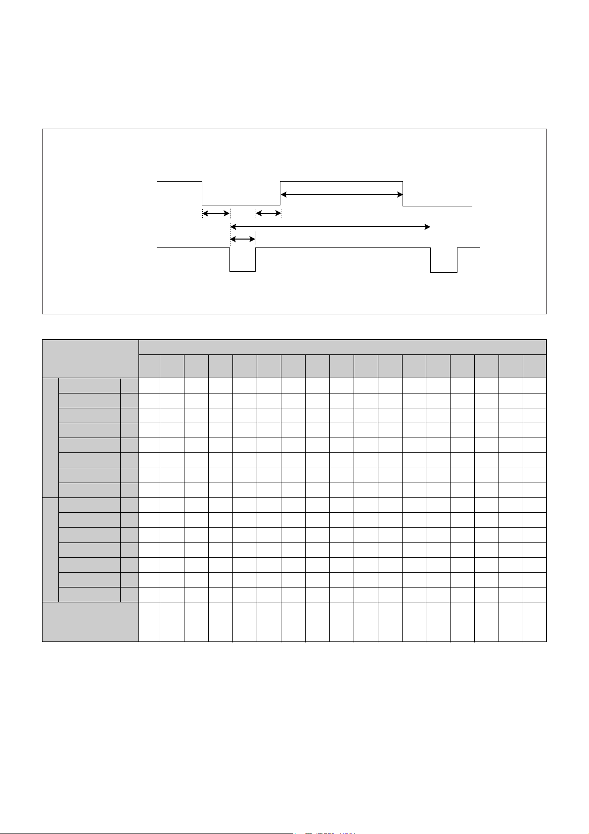
3. SIGNAL (Refer to the Timing Chart)
3-1. Sync Signal
1) Type : Separate Sync. (Horizontal & Vertical)
2) Input Voltage Level : Low=0~0.8V, High=2.1~5.5V
3) Sync Polarity : Positive or Negative
3-2. Video Input Signal
1) Type : R, G, B Analog
2) Voltage Level : 0~0.714 V
a) Color 0, 0 : 0 Vp-p
b) Color 7, 0 : 0.467 Vp-p
c) Color 15, 0 : 0.714 Vp-p
3) Input Impedance : 75 ½
3-3. Operating Frequency
Horizontal : 31 ~ 80kHz
Vertical : 58 ~ 85Hz
4. POWER SUPPLY
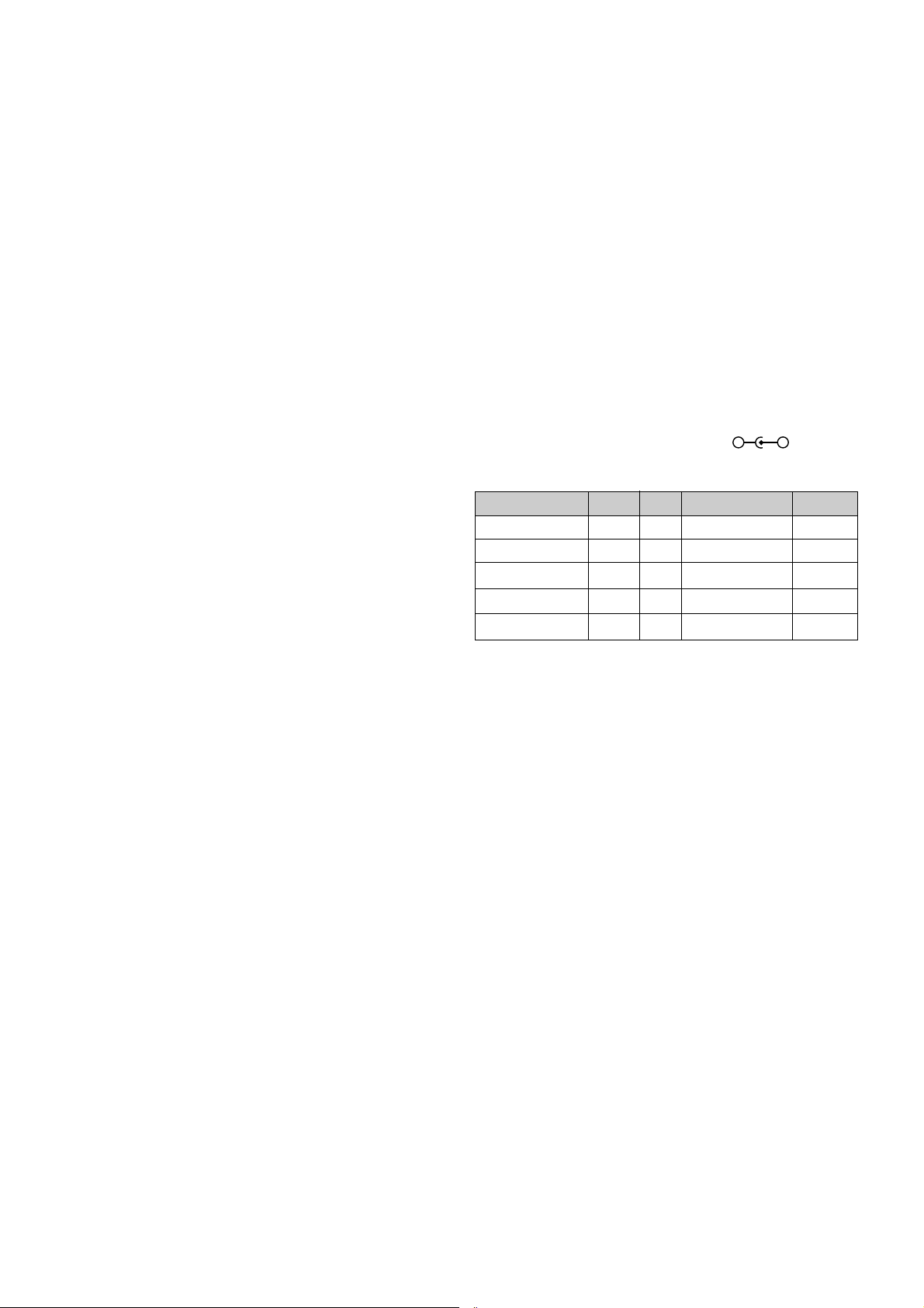
4-1. Power Adaptor
Input : AC 100~240V, 50/60Hz 1.2A
Output : DC 12V 5.0A
4-2. Power Consumption
5. ENVIRONMENT
5-1. Operating Temperature: 10¡C~30¡C (50¡F~95¡F)
(Ambient)
5-2. Relative Humidity : 10%~80%
(Non-condensing)
5-3. Altitude : 0~10,000ft (3,030m)
6. DIMENSIONS (with TILT/SWIVEL)
Width : 432.0mm (17.01'')
Depth : 247.1mm (9.73'')
Height : 446.6mm (17.58'')
7. WEIGHT (with TILT/SWIVEL)
Net Weight : 9.2kg (20.28 lbs)
Gross Weight : 12.9kg (28.44 lbs)
- 2 -
MODE
POWER ON (NORMAL)
STAND-BY
SUSPEND
Sleep Timer Function
Active
POWER OFF
H/V SYNC
ON/ON
OFF/ON
ON/OFF
ON/ON
-
POWER CONSUMPTION
less than 60 W
less than 5 W
less than 5 W
less than 5 W
less than 5 W
LED COLOR
GREEN
ORANGE
ORANGE
Orange Flashing
at 0.5Hz
OFF
VIDEO
ACTIVE
OFF
OFF
ON
-
SPECIFICATIONS
-
+
- 4 -
VIDEO
SYNC
D
F
B
E
A
TIMING CHART
MODE
Resolution
H
O
R
I
Z
O
N
T
A
L
V
E
R
T
I
C
A
L
kHz
Pixels
Pixels
Pixels
Pixels
Pixels
Hz
Lines
Lines
Lines
Lines
Lines
+
25.175
31.469
800
640
16
96
48
-
70.8
449
350
38
2
59
MARK
E
A
B
D
F
E
A
B
D
F
Sync Polarity
Dot Clock
Frequency
Total Period
Video Active Time
Front Porch
Sync Duration
Back Porch
Sync Polarity
Frequency
Total Period
Video Active Time
Front Porch
Sync Duration
Back Porch
FACTORY PRESET MODE
640
X
350
71Hz
-
28.321
31.468
900
720
18
108
54
+
70.8
449
400
12
2
35
720
X
400
71Hz
-
25.175
31.469
800
640
16
96
48
-
59.94
525
480
10
2
33
640
X
480
60Hz
+
56.25
53.674
1048
800
32
64
152
+
85.061
631
600
1
3
27
800
X
600
85Hz
+
94.5
68.677
1376
1024
48
96
208
+
84.997
808
768
1
3
36
1024
X
768
85Hz
+/
-
100.0
68.681
1456
1152
32
128
144
+/
-
75.062
915
870
3
3
39
1152
X
870
75Hz
+/
-
92.978
61.805
1504
1152
18
134
200
+/
-
65.96
937
900
2
4
31
1152
X
900
65Hz
+
108.0
63.981
1688
1280
48
112
248
+
65.02
1066
1024
1
3
38
1280
X
1024
65Hz
+
135.0
79.976
1688
1280
16
144
248
+
75.035
1066
1024
1
3
38
1280
X
1024
75Hz
-
31.5
37.50
840
640
16
64
120
-
75.0
500
480
1
3
16
640
X
480
75Hz
-
36.0
43.269
832
640
56
56
80
-
85.0
509
480
1
3
25
640
X
480
85Hz
+
40.0
37.879
1056
800
40
128
88
+
60.32
628
600
1
4
23
800
X
600
60Hz
+
49.5
46.875
1056
800
16
80
160
+
75.0
625
600
1
3
21
800
X
600
75Hz
+/
-
57.283
49.725
1152
832
32
64
224
+/
-
74.55
667
624
1
3
39
832
X
624
75Hz
-
65.0
48.363
1344
1024
24
136
160
-
60.0
806
768
3
6
29
1024
X
768
60Hz
-
78.75
60.123
1312
1024
16
96
176
-
75.03
800
768
1
3
28
1024
X
768
75Hz
MODE1MODE2MODE3MODE4MODE5MODE6MODE7MODE8MODE9MODE10MODE11MODE12MODE13MODE14MODE15MODE
16
MHz
- 8 -
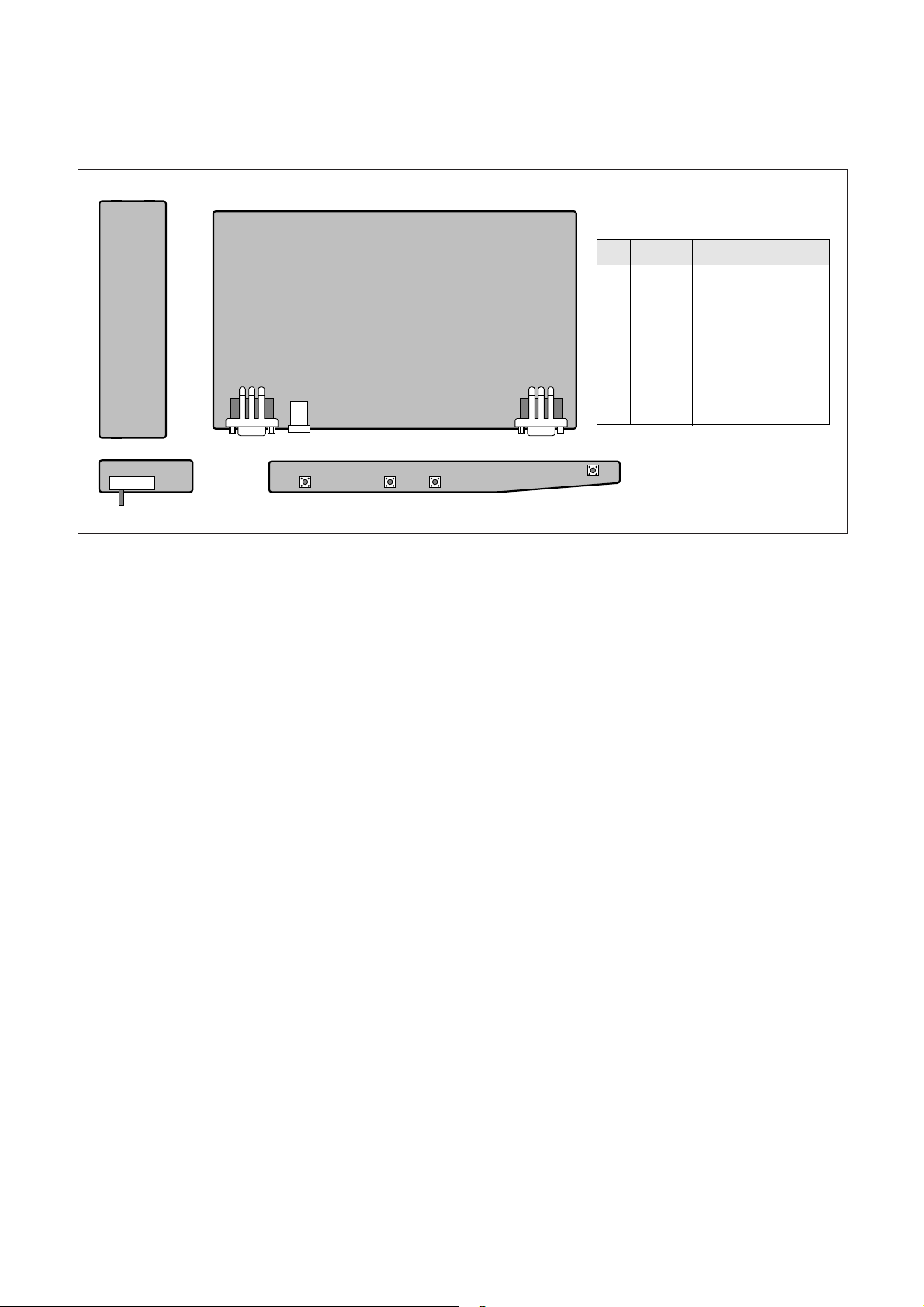
CONTROL LOCATIONS
1234
5
NO.
1
2
3
4
5
Ref. No.
SL-SW
SW01
SW02
SW03
SW04
Control Function
SLIDE SWITCH
MENU BUTTON
-
BUTTON
+ BUTTON
POWER SWITCH
- 8 -
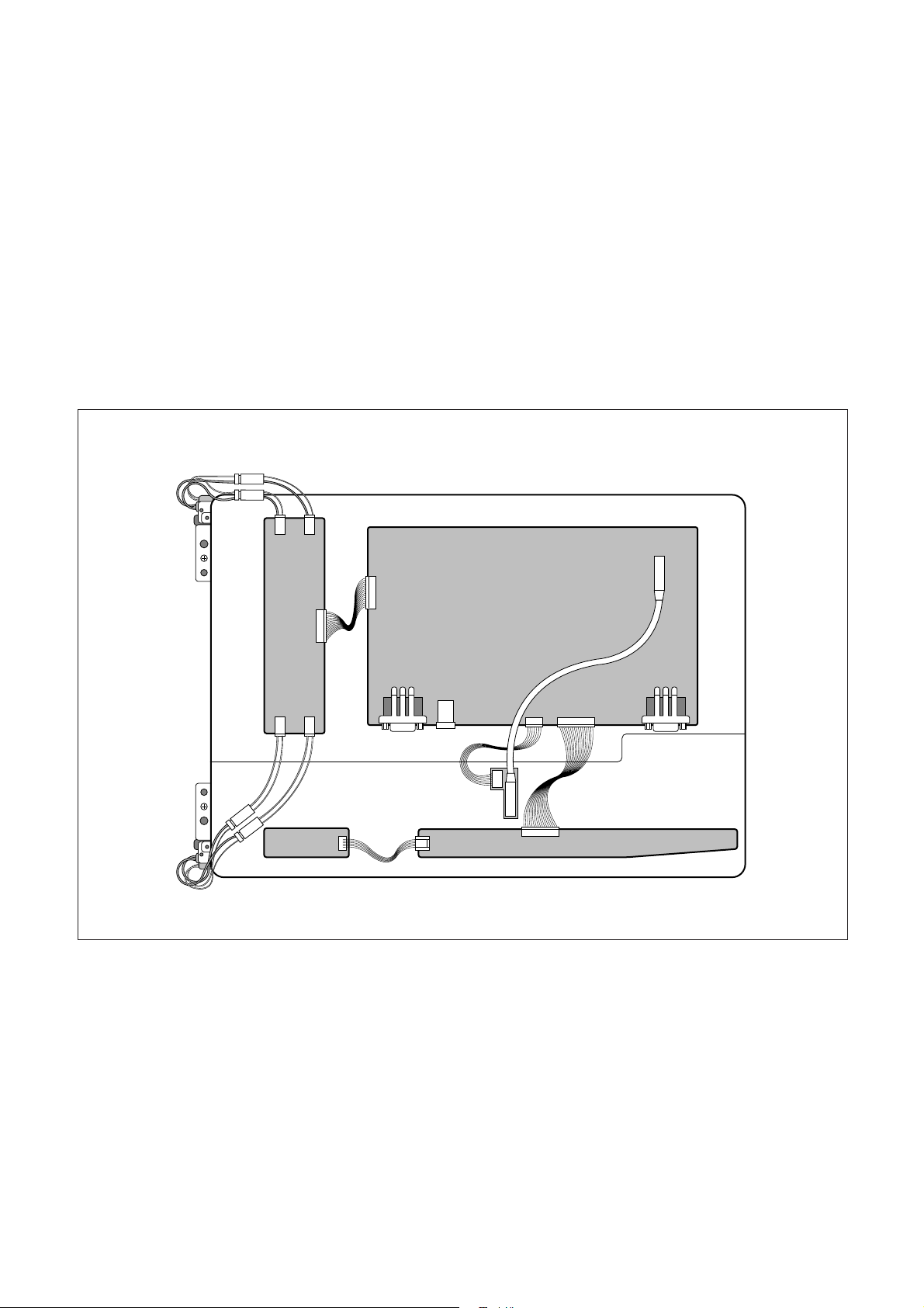
WIRING DIAGRAM
J07
J04
J1J2
J3J4
J5
CN2
J05 J06
P02
P01P02
CN1
DISASSEMBLY
- 9 -
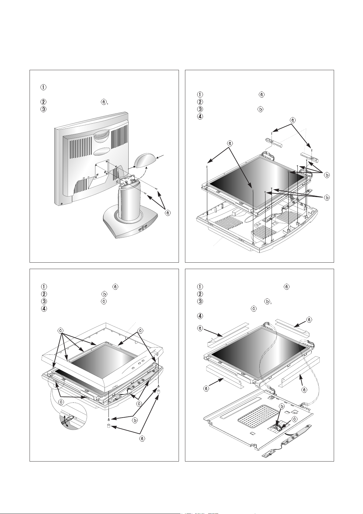
1. TILT/SWIVEL REMOVAL
Remove Hinge Cover (Push the tilt cover
both side).
Remove two screws
Remove the Tilt/swivel.
2. FRONT CABINET REMOVAL
Remove two screws cap .
Remove two screws .
Release ten latches .
Remove the Front Cabinet.
3. INVERTER WIRE SHIELD & BACK COVER
REMOVAL
Remove four screws .
Remove two Inverter Wire Shield.
Remove five screws .
Remove the Back Cover.
4. LCD MODULE REMOVAL
Remove four Aluminum Tapes .
Disconnect J1, J2, J3 and J4.
Disconnect FPC Cable and Module
Power Connector
.
Remove the LCD Module.
Front Cabinet
Inverter
Wire Shield
Back Cover
- 10 -
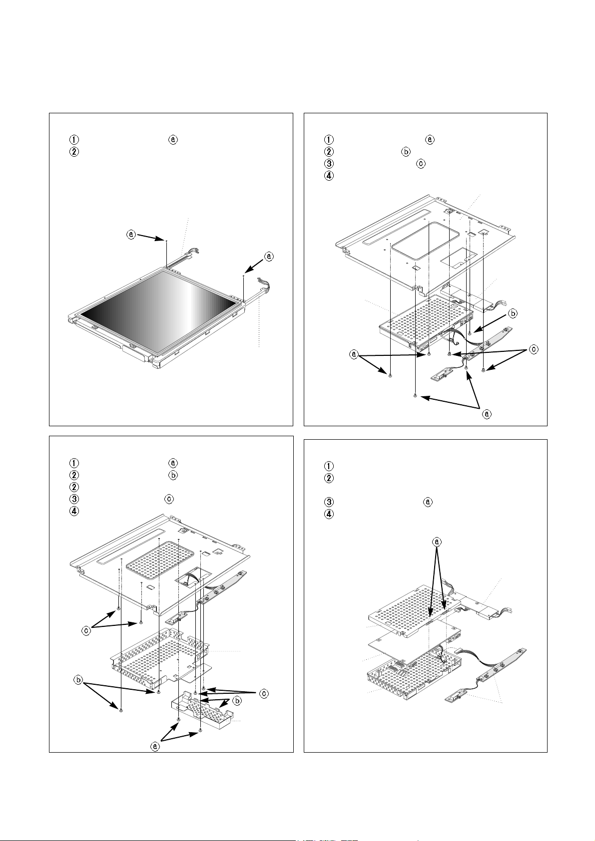
6. INVERTER FRAME & REAR SHIELD REMOVAL
Remove two screws .
Release two latches .
Remove the Inverter Shield.
Remove six screws .
Remove the Rear Shield.
5. BACKLIGHT REMOVAL
Remove two screws .
Remove the Backlight from the LCD Module.
7. MAIN FRAME REMOVAL
Remove four screws .
Remove screw .
Remove two fixers .
Divide the Main PCB AssÕy.
8. MAIN TOTAL ASSÕY REMOVAL
Disconnect J5 and J06.
Remove Inverter AssÕy and Control PCB
from the Main PCB.
Release two latches .
Divide Top Shield, Main PCB, and Bottom Shield.
Bottom (Lower) Backlight AssÕy
Top (Upper) Backlight AssÕy
Rear Frame
Inverter Frame
Main Frame
Inverter PCB
Main PCB
AssÕy
PCB Shield
(Bottom)
Control PCB
Inverter AssÕy
Main PCB
PCB Shield
(Top)
EXPLODED VIEW
2
3
4
5
6
7
8
9
10
11
12
14
a
b
c
c
c
c
c
d
d
e
5-1
5-2
5-3
14-1
13
1
a
15
16
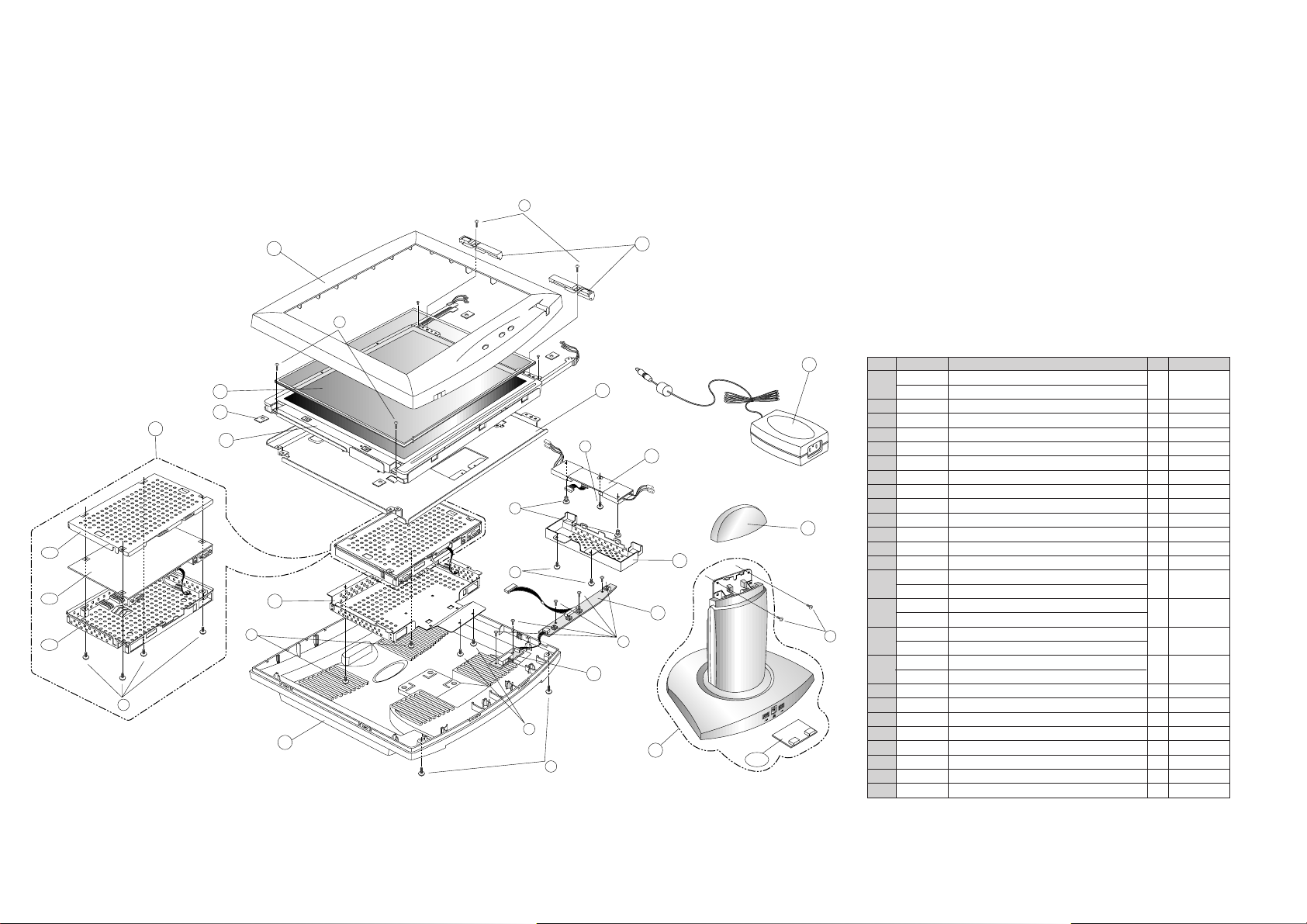
EXPLODED VIEW PARTS LIST
Ref. No.
1
2
3
4
5
5-1
5-2
5-3
6
7
8
9
10
11
12
13
14
14-1
15
16
a
b
c
d
e
Part No.
3091TKL004A
3091TKL004B
6304TLT181A
4814TKK064A
4951TKS034A
3313TL8001A
4950TKK049A
6871TMT077A
4950TKK048D
6633TZA002A
4814TKK067A
4950TKS097A
6871TST084A
6871TST089A
3809TKL004A
3809TKL004B
6634TBZ002A
6634TBZ002B
3550TKK044A
3550TKK044B
3043TKK034A
3043TKK034B
6871TST081A
3550TKK046B
4819TKK082A
332-015E
4930TKK014A
332-110A
332-095C
332-105F
Description
CABINET ASSÕY, OPAL COMPAQ LCD 18.1Ó
CABINET ASSÕY, CARBON BLACK COMPAQ LCD 18.1Ó
LCD MODULE, LGE TFT LCD LM181E1 18.1Ó
INVERTER WIRE SHIELD
METAL, MAIN FRAME
MAIN TOTAL ASSÕY
PCB SHIELD (BOTTOM)
MAIN PCB ASSÕY
PCB SHIELD (TOP)
INVERTER ASSÕY
INVERTER SHIELD
METAL, REAR FRAME
KEY CONTROL PCB ASSÕY
S/W PCB ASSÕY
BACK COVER ASSÕY, OPAL
BACK COVER ASSÕY, CABON BLACK
ADAPTER, AC-DC, 100/240V 12V 5A, OPAL
ADAPTER, AC-DC, 100/240V 12V 5A, CABON BLACK
HINGE COVER, OPAL
HINGE COVER, CABON BLACK
TILT SWIVEL ASSÕY, OPAL
TILT SWIVEL ASSÕY, CABON BLACK
USB PCB ASSÕY
PROTECTIVE PANEL COVER - PROTECTIVE MODEL ONLY
BRACKET, SUPPORT MODULE - NON PROTECTIVE MODEL
SCREW, PVS+3x16 (MSWR/FZMW)
HOLDER, FIXER
SCREW, PZS+3x6 (MSWR/FZMY)
SCREW, PZP+3x12 (MSWR/FZMY)
SCREW, PVS+4x10 (MSWR/FZMW)
Q'ty
1
1
2
1
1
1
1
1
1
1
1
1
1
1
1
1
1
1
1
4
4
2
13
7
2
Material
BLOCK DIAGRAM
- 11 -
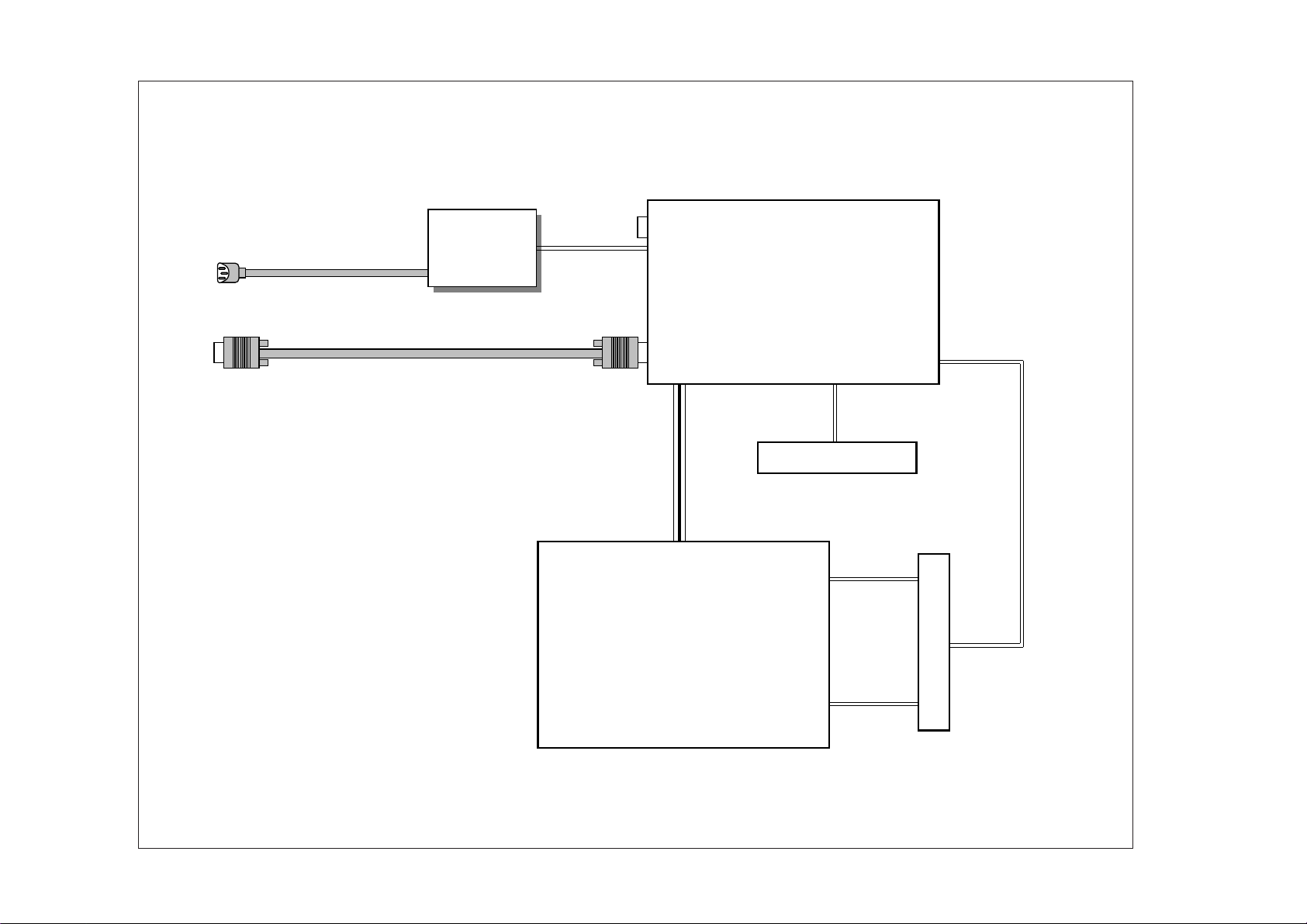
POWER CORD
15-pin D-SUB SIGNAL CABLE
POWER
SUPPLY
CONTROL PCB
INVERTER PCB
MAIN LOGIC
PCB
LCD MODULE
System Block Diagram
BLOCK DIAGRAM
- 12 -
Data
Clock
Memory
Flat panel
Controller
Display
Data
Transmitter
LCD
Module
KM416S102BT
MX88272
BA7657F
TDA4885
LVDS83
LM181E1
MCLK
H
H
H
V
V
V
V
5V
3.3V 5V 3.3V 3.3V
5V
5V
3.3V
8V
12V
5V
Even
Even
DS
H-Sync
H-Sync
CLK
. Contrast
Odd
Odd
CLAMP
SDA/SCL
CS/SDA/SCL
D-F/F
TT'L
Gate
Power
12V
Input Switch
Pre-Amp.
Inverter
Clock
Generator
DC/DC
Converter
AD9483
ICS1522
MAX785
A/D Converter
Micro-
Controller
Input Port "A"
Input Port "B"
. Brightness
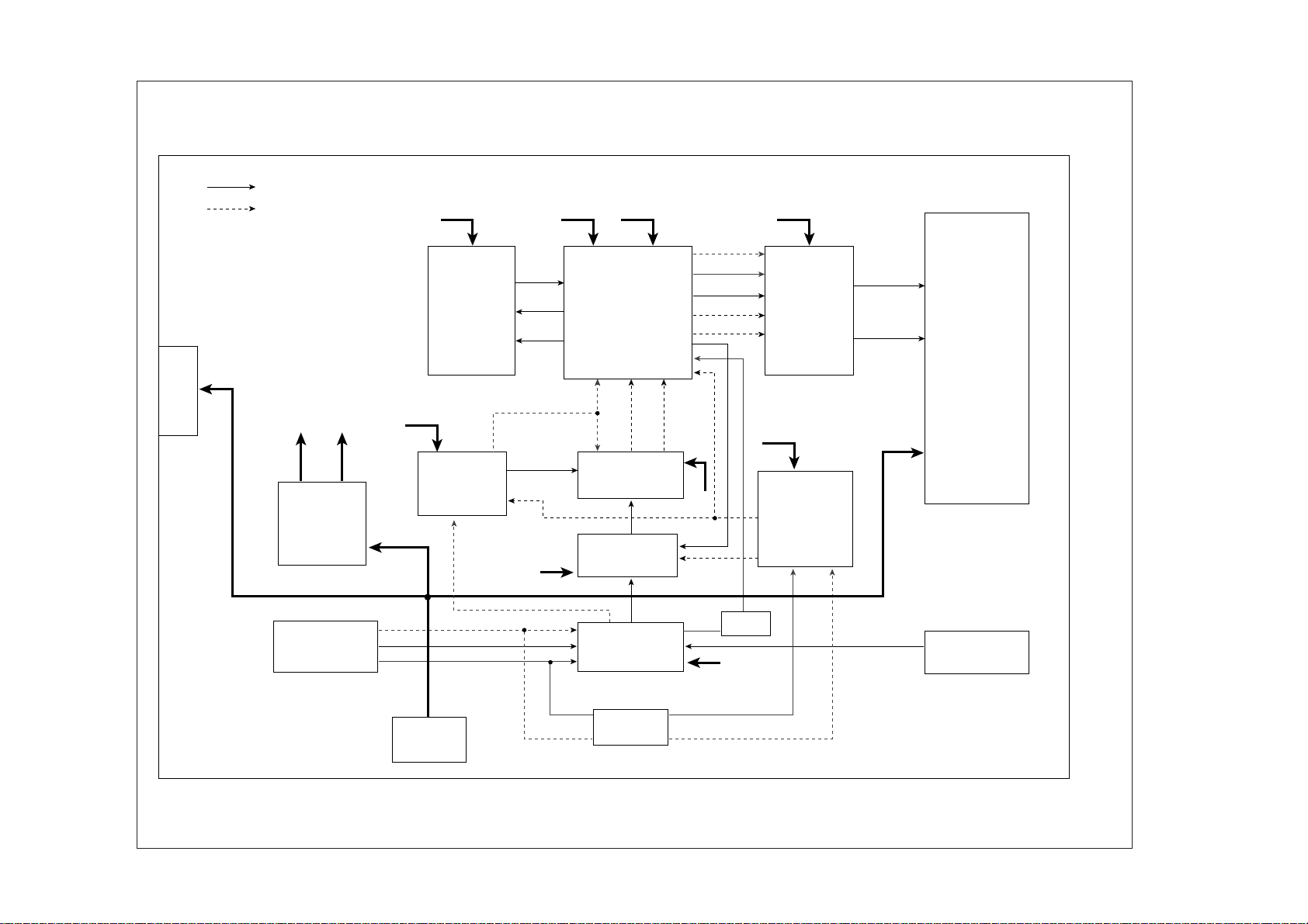
Block Diagram for Main Logic Board

DESCRIPTION OF BLOCK DIAGRAM
1. Video Control Circuit
1) TDA4885 (U101) receives the video signal from PC
and amplifies the levels of video signal (0V~0.7V), and
controls the contrast signal.
2) The biases of A/D inputs control the reference output
voltages of TDA4885 (U101) to proper R, G, B bias
levels through the Diodes (D101, D102, D103).
4) The EX-OR (U604) device outputs the voltage levels to
decide the polarities of HSYNCIN and VSYNCIN that
supply the sync signals to the PLL IC and MICOM.
2. A/D Converter Circuit
1) AD9483 (U201) converts from the analog video signal
to the digital signal. For this function, its DC 2.5V
output is connected to VREF_IN and it samples the
input signal between 2.0V~3.0V. (The reference
voltage of the sampling is 2.5V.)
2) The frequency range of 8-bit digital output is from
12.5MHz to 67.5MHz with respect to modes.
3) The status of power down pin is low for normal state
and high for power down state.
3. Features of ICS1522 PLL IC
1) ICS1522 (U11) generates the pixel clock for each
mode with respect to internal register setting, which is
used to sampling circuitry.
The range of the pixel clock is approximately from
25MHz to 135MHz
4. Video Process Circuit
This circuit consists of MXIC (U501) and frame
memorys (U401, 402, 403) which convert frame date
of input signal to 60Hz frame date. This function is
processed by MX88272. The MX88272 (U501) gets
the video signal converted analog to digital,
interpolates input to 1280x1024 resolution signal and
outputs 8-bit R, G, B, DHS, DVS and DE signals to the
transmitter (U701, U702).
5. LVDS Circuit
LVDS transmitter (U701, U702) delivers digital signal
to the receiver of module by the voltage swing of 1V.
The peripheral circuitry of transmitter gets the DHS,
DVS, DEN, DISPCLK signal, outputs LVDS signal. At
the power down mode, MICOM lets the power down
signal be low and Shuton pin be active low.
6. Input Switching Circuit
This circuit consists of BA7657F (U601), slide switch
and TTL gates. BA7657F (U601) switch analog R, G,
B signal to be entered form 15p D-SUB A(J2) or B(J3).
If the position of slide switch is A; R, G, B signal and
H/V Sync are entered from D-SUB A. If the Position of
slide switch is B; R, G, B signal and H/V sync are
entered from D-SUB B. If the position of slide switch is
Auto; R, G, B signal and H/V sync are automatically
selected A or B by control signal of MICOM. But if A
and B are incidentally connected, system display OSD,
Ò2 Input active... select A or BÓ.
TTL gates (U602, U603, U604) switch H/V sync to be
entered from D-SUB A or B.
7. DC/DC Converter
This curcuit supplies stand-by 5V (5VST) that is made
using IC U801 regulator for MICOM and SYNC
processing.
The 5VDD voltage is converted using MAX785 (U802)
and supply to IC need to it.
The 8VA is converted using 8V regulator (U808) and
supply to video pre-amp.
The 3.3V voltage is converted using 6 Diodes and
supply to IC need to it.
The 5VA is converted using 5V regulator (U809) and
supply to A/D converter and PLL IC.
The state of power down make all voltage except
5VST down using SHDN.
8. System Controller (08XL36) Circuit
This curcuit consists of EEPROM IC (U902) which
stores control data, RESET IC (U904) and LED driver
Q01 and Q02 indicate that power is ON or OFF.
The operating procedures of MICOM and its
associated circuit are as follows:
- 13 -

1) The MICOM distinguishes polarity and frequency of
the horizontal sync and the vertical sync are supplied
from signal cable. The controlled data of each mode is
stored in EEPROM.
2) User can adjust screen condition by each OSD
function. (H-Position, V-Position, Clock, Clock Phase,
... etc.)
9. DDC Circuit
This circuit consists of MICOM (U901) and bidirection
switching IC (U2).
1) Bidirection switching IC switch I
2
C line for DDC
communication by control signal of MICOM (U901).
2) The MICOM has D-SCL, D-SDA line for sending and
receiving data to adjust line through 15-pin D-sub
connector.
3) The data of EDID DDC information is stored in
EEPROM IC (U902).
10. OSD Control Circuit
When the MX88272 outputs the area which is able to
display overlay using OSDBLNK PIN of MX88272.
OSD (On-Screen-Display) device (U502) outputs
display data as the timing of the signal.
11. Power Module Circuit
This block supplies the +12V to the inverter for the
backlight voltage of module and the +5V for data
control of LCD module.
That is, SI4925DY (Q01) is switched by TR Q12 for
module voltage.
- 14 -
 Loading...