

LG LP173WF2-TPA1 Schematics
( ) Preliminary Specification
( ● ) Final Specificatio n
LP173WF2
Liquid Crystal Display
Product Specification
SPECIFICATION
FOR
APPROVAL
Title
BUYER DELL
MODEL
APPROVED BY
/
/
/
SIGNATURE
17.3” Full HD TFT LCD
SUPPLIER LG Display Co., Ltd.
*MODEL LP173WF2
Suffix TPA1
*When you obtain standard approval,
please use the above model name without suffix
APPROVED BY SIGNATURE
J. Y. Lee / Manager
REVIEWED BY
S. W. Park / Engineer
PREPARED BY
H. M. Yoon / Engineer
J. H. Shin / Engineer
Please return 1 copy for your confirmation with
your signature and comments.
Ver. 1.2 May. 4. 2011
Product Engineering Dept.
LG Display Co., Ltd
Product Specification
Contents
LP173WF2
Liquid Crystal Display
No
1
2
3
3-1
3-2
3-3
3-4
3-5
3-6
3-7
COVER
CONTENTS
RECORD OF REVISIONS
GENERAL DESCRIPTION
ABSOLUTE MAXIMUM RATINGS
ELECTRICAL SPECIFICATIONS
ELECTRICAL CHARACTREISTICS
INTERFACE CONNECTIONS
eDP SIGNAL TIMING SPECIFICATION
SIGNAL TIMING SPECIFICATIONS
SIGNAL TIMING WAVEFORMS
COLOR INPUT DATA REFERNECE
POWER SEQUENCE
ITEM
Page
1
2
3
4
5
6-7
8
9-10
11
11
12
13
4
5
6
7
7-1
7-2
7-3
8
8-1
8-2
9
Ver. 1.2 May. 4. 2011
OPTICAL SFECIFICATIONS
MECHANICAL CHARACTERISTICS
RELIABLITY
INTERNATIONAL STANDARDS
SAFETY
EMC
Environment
PACKING
DESIGNATION OF LOT MARK
PACKING FORM
PRECAUTIONS
A APPENDIX. Enhanced Extended Display Identification Data
14-17
18-21
27
28
28
28
29
29
30-31
32-34
2/ 34
Product Specification
RECORD OF REVISIONS
LP173WF2
Liquid Crystal Display
Revision No Revision Date Page Description
0.0 May. 10. 2010 - First Draft (Preliminary Specification) -
0.1 May. 19. 2010 8 Updated Connector pinmap (#50) 10 Updated T iming table
19 Updated Rear view
0.2 Aug. 11.2010
20 Updated Label information
31 Updated ED ID data
0.3 Sep. 10. 2010 6 Updated Power Consumption 13 Updated O ptical Spec.
15 Updated G ray scale
0.4 Sep. 28, 2010 31-33 Updated EDID File (Check sum : A3 DB) 0.4
0.5 Oct. 21, 2010 31~33 Updated EDID File (color coordinates) 0.5
10 Insert the Eye diagram Spec.
1.0 Dec. 17. 2010
1.1 Jan. 7, 2011 20 Updated M echanic diagram
1.2 May. 4. 2011 - Updated Revision (A01 → A02)
EDID
ver
0.3
1.0 32~34 Updated EDID File (Check sum : DB 27 )
Ver. 1.2 May. 4. 2011
3/ 34
LP173WF2
Liquid Crystal Display
Product Specification
1. General Description
The LP173WF2 is a Color Active Matrix Liquid Crystal Display with an integral LED backlight system. The
matrix employs a-Si Thin Film Transistor as the active element. It is a transmissive type display operating in
the normally white mode. This TFT-LCD has 17.3 inches diagonally measured active display area with FHD
resolution (1920 horizontal by 1080 vertical pixel array). Each pixel is divided into Red, Green and Blue subpixels or dots which are arranged in vertical stripes. Gray scale or the brightness of the sub-pixel color is
determined with a 6-bit gray scale signal for each dot, thus, presenting a palette of more than 262,144
colors. The LP173WF2 has been designed to apply the interface method that enables low power, high
speed, low EMI. The LP173WF2 is intended to support applications where thin thickness, high brightness
are critical factors and graphic displays are important. In combination with the vertical arrangement of the
sub-pixels, the LP173WF2 characteristics provide an excellent flat display for office automation products
such as Notebook PC.
VOUT_LED
VLED
LED_EN
PWM
User connector
AUX
eDP
4Lane
LED Driver
Block
eDP Timing Control
(Tcon) Block
FB1~6
FB7~12
LED Backlight Ass’y
1
TFT-LCD Panel
1920
(FHD, Dual Gate COF , TN)
1080
EDID signal & Power
50
Pin
VCC +5V
AVCC
DVCC
TVCC
Power
Block
FLK
DPM
GSC
VGH, VGL, GMA
GSP
GOE
GSC
Mini-LVDS
AVCC, AVDD
Control & Data Power
General Features
Active Screen Size 17.3 inches diagonal
Outline Dimension
Pixel Pitch
Pixel Format 1920 horiz. by 1080 vert. Pixels RGB strip arrangement
Color Depth 6-bit, 262,144 colors
Luminance, White 400 cd/m
Power Consumption Total 60Hz : 16.3W, Total 120Hz + VBI32% : 20 W (Typ.)
Weight 650g (Max.)
Display Operating Mode Transmissive mode, normally white
Surface Treatment Glare treatment of the front Polarizer
RoHS Compliance Yes
BFR / PVC / As Free Yes for all.
Ver. 1.2 May. 4. 2011
381.888(Typ. H) × 214.812(Typ. V) × 6.5(D, Max.) [mm]
0.199 × 0.199 mm
2
(Typ.)
Source Driver
(Bottom Bent)
4/ 34
LP173WF2
Liquid Crystal Display
Product Specification
2. Absolute Maximum Ratings
The following are maximum values which, if exceeded, may cause faulty operation or damage to the unit.
Table 1. ABSOLUTE MAXIMUM RATINGS
Parameter Symbol
Power Input Voltage
Operating Temperature
Storage Temperature
Operating Ambient Humidity
Storage Humidity
VCC -0.3 4.0 Vdc at 25 ± 5°C
TOP 0 50 °C 1
HST -20 60 °C 1
HOP 10 90 %RH 1
HST 10 90 %RH 1
Values
Units Notes
Min Max
Note : 1. Temperature and relative humidity range are shown in the figure below.
Wet bulb temperature should be 39
Wet Bulb
Temperature [℃]
30
20
10
0
°C Max, and no condensation of water.
90% 80%
60
50
40
60%
Humidity[(%)RH]
40%
20%
10%
Storage
Operation
-20
10
20 30 40 50
60 70 80 0
Dry Bulb Temperature [℃]
Ver. 1.2 May. 4. 2011
5/ 34
LP173WF2
Liquid Crystal Display
Product Specification
3. Electrical Specifications
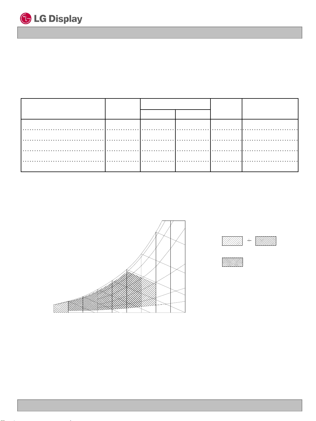
3-1. Electrical Characteristics
The LP173WF2 requires two power inputs. The first logic is employed to power the LCD electronics and to
drive the TFT array and liquid crystal. The second backlight is the input about LED BL with LED Driver.
Table 2. ELECTRICAL CHARACTERISTICS
Parameter Symbol
Min Typ Max
LOGIC :
Values
Unit Notes
Power Supply Input Voltage V
Power Supply Input Current (2D) Mosaic I
CC 4.5 5.0 5.5 V 1
CC - 750 880
mA
Power Supply Input Current (3D) Mosaic I
Power Consumption (2D) Mosaic P
CC - 1300 1500
CC - 3.8 4.4
W
Power Consumption(3D) Mosaic P
Power Supply Inrush Current I
eDP Impedance Z
CC - 6.5 7.5
CC_P - - 2000 mA 4
eDP 90 100 110 Ω 5
BACKLIGHT : ( with LED Driver)
LED Power Input Voltage V
LED Power Input Current I
LED Power Consumption P
LED Power Inrush Current I
LED 7.0 12.0 21.0 V 6
LED - 960 1000 mA 7
LED - 11.5 12 W 7
LED_P - - 1000 mA 8
PWM Duty Ratio 5 - 100 %
PWM Jitter
PWM Impedance Z
PWM Frequency F
PWM High Level Voltage V
PWM Low Level Voltage V
LED_EN Impedance Z
-
PWM 450 500 550 kΩ
PWM
PWM_H
PWM_L
PWM 450 500 550 kΩ
0 - 0.2 % 10
200 - 1000 Hz
3.0 - 3.6 V
0 - 0.3 V
2
9
11
LED_EN High Voltage V
LED_EN Low Voltage V
LED_EN_H 3.0 - 3.6 V
LED_EN_L 0 - 0.3 V
Life Time 12,000 - - Hrs 12
Ver. 1.2 May. 4. 2011
6/ 34
Liquid Crystal Display
Product Specification
Note)
1. The measuring position is the connector of LCM and the test conditions are under 25℃, fv = 60Hz.
2. The specified Icc current and power consumption are under the Vcc = 5V , 25℃, fv = 60Hz or
120Hz+VBI condition.
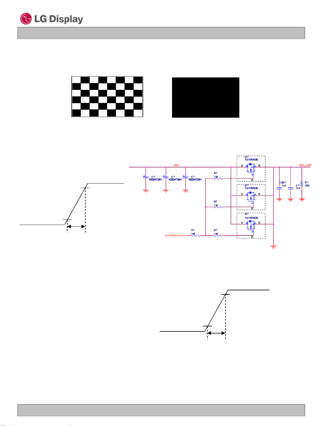
White Pattern Black Pattern
3. This Spec. is the max load condition for the cable impedance designing.
4. The below figures are the measuring Vcc condition and the Vcc control block LGD used.
The Vcc condition is same as the minimum of T1 at Power on sequence.
LP173WF2
Rising time
Vcc
0V
10%
90%
3.3V
0.5ms
5. This impedance value is needed for proper display and measured from eDP Tx to the mating connector.
6. The measuring position is the connector of LCM and the test conditions are under 25℃.
7. The current and power consumption with LED Driver are under the Vled = 12.0V , 25℃, Dimming of
Max luminance and White pattern with the normal frame frequency operated(60Hz).
8. The below figures are the measuring Vled condition
and the Vled control block LGD used.
VLED control block is same with Vcc control block.
Rising time
V
LED
90%
12.0V
0V
10%
0.1ms
9. The operation of LED Driver below minimum dimming ratio may cause flickering or reliability issue.
10. If Jitter of PWM is bigger than maximum, it may induce flickering.
11. This Spec. is not effective at 100% dimming ratio as an exception because it has DC level equivalent
to 0Hz. In spite of acceptable range as defined, the PWM Frequency should be fixed and stable for
more consistent brightness control at any specific level desired.
12. The life time is determined as the time at which brightness of LCD is 50% compare to that of minimum
value specified in table 7. under general user condition.
Ver. 1.2 May. 4. 2011
7/ 34
LP173WF2
Liquid Crystal Display
Product Specification
3-2. Interface Connections
This LCD employs two interface connections, a 50 pin connector used for the module electronics interface and
the other connector used for the integral backlight system.
Table 3. MODULE CONNECTOR PIN CONFIGURATION (CN1)
Pin Symbol Description Notes
1 NC
2 NC Reserved
3 GND Ground
4 Lane3_N Signal Link Lane3
5 Lane3_P Signal Link Lane3
6 GND Ground
7 Lane2_N Signal Link Lane2
8 Lane2_P Signal Link Lane2
9 GND Ground
10 Lane1_N Signal Link Lane1
11 Lane1_P S i gnal Li nk Lane1
12 GND Ground
13 Lane0_N Signal Link Lane0
14 Lane0_P S i gnal Li nk Lane0
15 GND Ground
16 AUX_CH_P Signal Auxiliary Ch.
17 AUX_CH_N Signal Auxiliary Ch.
18 GND Ground
19 Vcc LCD logic input power
20 Vcc LCD logic input power
21 Vcc LCD logic input power
22 Vcc LCD logic input power
23 Vcc LCD logic input power
24 Vcc LCD logic input power
25 Vcc LCD logic input power
26
27 Vcc LCD logic input power
28 Vcc LCD logic input power
29 GND Ground
30 GND Ground
31 GND Ground
32 GND Ground
33 Bist Bist
34 GND Ground
35 HPD Hot plug Detection P i n
36 GND Ground
37 GND Ground
38
39 GND Ground
40
41
42
43
44 GND Ground
45
46
47
48
49 GND Ground
50
Vcc LCD
GND
LED_EN Backlight On/Off Control
PWM PWM for luminance control
NC Reserved
NC Reserved
VLED LED Power Supply 7V-21V
VLED LED Power Supply 7V-21V
VLED LED Power Supply 7V-21V
VLED LED Power Supply 7V-21V
NC
Reserved
logic input power
Ground
Reserved
[Interface Chip]
1. LCD :
MStar, MST7339Y(LCD Controller)
Including eDP Receiver.
2. System : ANX9806 or equivalent
[Connector]
JAE FI-VHP50 or equivalent
[Mating Connector]
JAE FI-VHP50 series or equivalent
(micro-coax type)
[Connector pin arrangement]
50
[LCD Module Rear View]
40
[LCD Module Rear View]
1
1
Ver. 1.2 May. 4. 2011
8/ 34
LP173WF2
Liquid Crystal Display
Product Specification
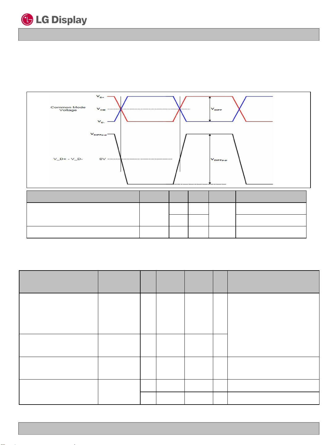
3-3. eDP Signal Timing Specifications
3-3-1. DC Specification
The VESA Display Port related AC specification is compliant with the VESA Display Port Standard v1.1a.
Description Symbol Min Max Unit Notes
Differential peak-to-peak Input voltage
VDIFF p-p
120 -
mV
For high bit rate
40 - For reduced bit rate
Rx DC common mode voltage V
CM
0 2.0 V -
3-3-2. AC Specification
The VESA Display Port related AC specification is compliant with the VESA Display Port Standard v1.1a.
Description Symbol Min Typ Max Unit Notes
Unit Interval for high bit rate
(2.7Gbps/lane)
Unit Interval for high bit rate
(1.62Gbps/lane)
Lane-to-Lane skew
UI_High_Rate - 370 - ps
UI_Low_Rate - 617 - ps
V Rx-SKEWINTER_PAIR
- - 5200 ps -
Range is nominal ±350ppm.
DisplayPort Link Rx does not
require local crystal for link
clock generation
Lane intra-pair skew
Ver. 1.2 May. 4. 2011
V Rx-SKEWINTRA_PAIR
- - 100 ps For high bit rate
- - 300 ps For reduced bit rate
9/ 34
LP173WF2
Liquid Crystal Display
Product Specification
3-3-3. Eye Diagram
The VESA Display Port related Eye Diagram is compliant with the VESA Display Port Standard v1.1a.
2
1
4
3
Main Link Position Spec.
Lane 0
~
Lane 3
Lane 0
~
Lane 3
Point2
~
Point4
Point1
~
Point3
Min 150mV
(2.7Gbps,
min 188.33ps)
Ver. 1.2 May. 4. 2011
10/ 34
LP173WF2
Liquid Crystal Display
Product Specification
3-4. Signal Timing Specifications
This is the signal timing required at the input of the User connector. All of the interface signal timing should be
satisfied with the following specifications and specifications of eDP Tx/Rx for its proper operation.
Table 4. TIMING TABLE
ITEM Symbol Min. Typ. Max. Unit Note
2D
DCLK Frequency
f
CLK
- 37.1 100
MHz
(148.5MHz@60Hz)
3D
(396MHz@120+VBI)
Period
Hsync
Width
Width-Active
Period
Vsync
Width
Width-Active
Horizontal back porch
Data
Enable
Horizontal front porch
Vertical back porch
Vertical front porch
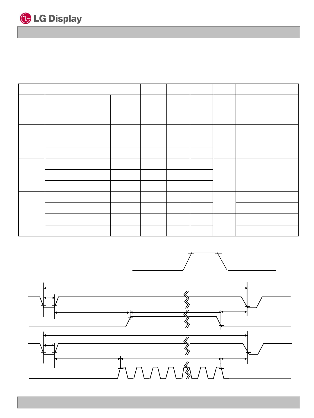
3-5. Signal Timing Waveforms
Data Enable, Hsync, Vsync
Hsync
tWH
t
HP
tWH
tw
HA
tVP
tWV
twVA
t
HBP
t
HFP
t
VBP
t
VFP
520 550 550
5 11 11
480 480 480
1120 1125 1980
5 5 5
1080 1080 1080
30 37 37
5 22 22
32 36 892
3 4 5
High: 0.7VCC
Low: 0.3VCC
t
HP
tCLK
tHP
tCLK
tHP
tWHA
Data Enable
t
WV
Vsync
Data Enable
t
HBP
tVP
t
VBP
Ver. 1.2 May. 4. 2011
tWVA
t
t
HFP
VFP
11/ 34
 Loading...