

Product Specification
SPECIFICATION
LP156WH9
Liquid Crystal Display
FOR
APPROVAL
)
(
(
Preliminary Specification
◆
)
Final Specification
MODEL
www.jxlcd.com
15.6” HD TFT LCDTitle
LGECustomer
*When you obtain standard approval,
www.jxlcd.com
please use the above model name without suffix
LG Display Co., Ltd.SUPPLIER
LP156WH9*MODEL
TLA1Suffix
SIGNATUREAPPROVED BY
/
/
/
Please return 1 copy for your confirmation with
your signature and comments.
Ver. 0.0 Mar. 8, 2011
APPROVED BY
APPROVED BY
J. Y. Lee / S.Manager
REVIEWED BY
REVIEWED BY
S. W. Park / Manager
PREPARED BY
PREPARED BY
H. M. Yoon / Engineer
J. H. Shin / Engineer
Products Engineering Dept.
LG Display Co., Ltd
SIGNATURE
SIGNATURE
1 / 32
Product Specification
Contents
LP156WH9
Liquid Crystal Display
No
COVER
CONTENTS
RECORD OF REVISIONS
1
2
3
3-1
3-2
3-3
3-3
3-4
3-5
3-6
4
GENERAL DESCRIPTION
ABSOLUTE MAXIMUM RATINGS
ELECTRICAL SPECIFICATIONS
ELECTRICAL CHARACTREISTICS
INTERFACE CONNECTIONS
LVDS SIGNAL TIMING SPECIFICATION
SIGNAL TIMING SPECIFICATIONS
SIGNAL TIMING WAVEFORMS
COLOR INPUT DATA REFERNECE
www.jxlcd.com
www.jxlcd.com
POWER SEQUENCE
OPTICAL SFECIFICATIONS-2D
ITEM
Page
1
2
3
4
5
6-7
8
9-10
11
11
12
13
14-16
4-1
5
Ver. 0.0 Mar. 8, 2011
OPTICAL SFECIFICATIONS-3D
MECHANICAL CHARACTERISTICS
APPENDIX. LPL PROPOSAL FOR SYSTEM COVER DESIGN A
RELIABLITY6
INTERNATIONAL STANDARDS7
SAFETY 7-1
EMC 7-2
ENVIRONMENT7-3
PACKING8
DESIGNATION OF LOT MARK 8-1
PACKING FORM 8-2
PRECAUTIONS9
APPENDIX. Enhanced Extended Display Identification Data A
17
18-21
22-24
25
26
26
26
27
27
28-29
30-32
2 / 32
Product Specification
RECORD OF REVISIONS
LP156WH9
Liquid Crystal Display
DescriptionPageRevision DateRevision No
First Draft (Preliminary Specification)-Mar. 8, 20110.0
www.jxlcd.com
www.jxlcd.com
EDID
ver
0.0
Ver. 0.0 Mar. 8, 2011
3 / 32
LP156WH9
Liquid Crystal Display
Product Specification
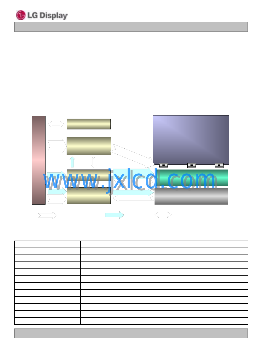
1. General Description
The LP156WH9 is a Color Active Matrix Liquid Crystal Display with an integral LED backlight system. The
matrix employs a-Si Thin Film Transistor as the active element. It is a transmissive type display operating in
the normally white mode. This TFT-LCD has 15.6 inches diagonally measured active display area with HD
resolution (1366 horizontal by 768 vertical pixel array). Each pixel is divided into Red, Green and Blue subpixels or dots which are arranged in vertical stripes. Gray scale or the brightness of the sub-pixel color is
determined with a 6-bit gray scale signal for each dot, thus, presenting a palette of more than 262,144
colors. The LP156WH9 has been designed to apply the interface method that enables low power, high
speed, low EMI. The LP156WH9 is intended to support applications where thin thickness, low power are
critical factors and graphic displays are important. In combination with the vertical arrangement of the subpixels, the LP156WH9 characteristics provide an excellent flat display for office automation products such as
Notebook PC.
User connector 40 Pin
www.jxlcd.com
www.jxlcd.com
General Features
EEPROM Block
for EDID
LVDS
1port
VCC
VLED
LED_EN
PWM
Control & Data Power
Timing Control
Block
DVCC
Power
Block
LED Driver
Block
15.6 inches diagonal Active Screen Size
359.3(H, typ) × 209.5(V, typ) × 5.6(D,max) [mm]Outline Dimension
0.252mm × 0.252 mmPixel Pitch
1366 horiz. By 768 vert. Pixels RGB strip arrangementPixel Format
6-bit, 262,144 colorsColor Depth
220 cd/m2(Typ.5 point @ PWM Duty = 100%)Luminance, White
Total 4.7 W(Typ.) Logic : 1.1W (Typ.@ Mosaic), B/L : 3.6W (Typ.@ VLED 12V )Power Consumption
465g (Max.)Weight
Transmissive mode, normally whiteDisplay Operating Mode
Glare treatment (3H) of the front Polarizer Surface Treatment
YesRoHS Comply
Yes for allBFR / PVC / As Free
CLKs
VGH, VGL, GMA
E
P
I
AVCC, AVDD
GIP CLKs, DSC
VOUT_LED
FB1~4
1
768
1366
TFT-LCD Panel
(FHD, GIP, TN)
Source Driver
(Bottom Bent)
LED Backlight Ass’y
EDID signal & Power
Ver. 0.0 Mar. 8, 2011
4 / 32
LP156WH9
Liquid Crystal Display
Product Specification
2. Absolute Maximum Ratings
The following are maximum values which, if exceeded, may cause faulty operation or damage to the unit.
Table 1. ABSOLUTE MAXIMUM RATINGS
Parameter Notes
Power Input Voltage
Operating Temperature
Storage Temperature
Operating Ambient Humidity
Storage Humidity
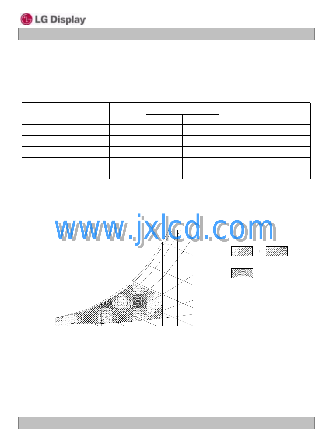
Note : 1. Temperature and relative humidity range are shown in the figure below.
Wet bulb temperature should be 39C Max, and no condensation of water.
Note : 2. Storage Condition is guaranteed under packing condition.
www.jxlcd.com
www.jxlcd.com
Wet Bulb
Temperature [℃]
20
10
0
Symbol
60
50
40
30
Values
MaxMin
90% 80%
60%
40%
20%
10%
Units
Humidity[(%)RH]
Storage
Operation
at 25 5CVdc4.0-0.3VCC
1C500TOP
1C60-20HST
1%RH9010HOP
1%RH9010HST
-20
Ver. 0.0 Mar. 8, 2011
10
20 30 40 50
Dry Bulb Temperature [℃]
60 70 800
5 / 32
LP156WH9
Liquid Crystal Display
Product Specification
3. Electrical Specifications
3-1. Electrical Characteristics
The LP156WH9 requires two power inputs. The first logic is employed to power the LCD electronics and to
drive the TFT array and liquid crystal. The second backlight is the input about LED BL.with LED Driver.
Table 2. ELECTRICAL CHARACTERISTICS
Values
SymbolParameter
MaxTypMin
LOGIC :
NotesUnit
1V3.63.33.0VCC Power Supply Input Voltage
2mA380335-ICC Mosaic Power Supply Input Current
2W1.31.1-PCC Power Consumption
3mA1500--ICC_P Power Supply Inrush Current
BACKLIGHT : ( with LED Driver)
www.jxlcd.com
www.jxlcd.com
PWM Jitter
PWM High Level Voltage
PWM Low Level Voltage
-
PWM_H
PWM_L
4Ω11010090ZLVDS LVDS Impedance
5V21.012.07.0VLED LED Power Input Voltage
6mA325300- ILED LED Power Input Current
6W3.853.6-PLED LED Power Consumption
7mA1500--ILED_P LED Power Inrush Current
8%100-5 PWM Duty Ratio
9%0.2-0
kΩ604020ZPWM PWM Impedance
10Hz1000-200FPWM PWM Frequency
V5.3-3.0V
V0.3-0V
kΩ604020ZPWM LED_EN Impedance
V5.3-3.0VLED_EN_H LED_EN High Voltage
Ver. 0.0 Mar. 8, 2011
V0.3-0VLED_EN_L LED_EN Low Voltage
11Hrs--15,000 Life Time
6 / 32
LP156WH9
Liquid Crystal Display
Product Specification
Note)
1. The measuring position is the connector of LCM and the test conditions are under 25℃, fv = 60Hz,
Black pattern.
2. The specified Icc current and power consumption are under
the Vcc = 3.3V , 25℃, fv = 60Hz condition and Mosaic pattern.
3. This Spec. is the max load condition for the cable impedance designing.
4. The below figures are the measuring Vcc condition and the Vcc control block LGD used.
The Vcc condition is same as the minimum of T1 at Power on sequence.
Rising time
Vcc
0V
www.jxlcd.com
5. This impedance value is needed for proper display and measured form LVDS Tx to the mating connector.
6. The measuring position is the connector of LCM and the test conditions are under 25℃.
7. The current and power consumption with LED Driver are under the Vled = 12.0V , 25℃, Dimming of
Max luminance and White pattern with the normal frame frequency operated(60Hz).
8. The below figures are the measuring Vled condition
and the Vled control block LGD used.
VLED control block is same with Vcc control block.
90%
10%
0.5ms
www.jxlcd.com
3.3V
Rising time
VLED
0V
10%
12.0V
90%
0.5ms
9. The operation of LED Driver below minimum dimming ratio may cause flickering or reliability issue.
10. If Jitter of PWM is bigger than maximum, it may induce flickering.
11. This Spec. is not effective at 100% dimming ratio as an exception because it has DC level equivalent
to 0Hz. In spite of acceptable range as defined, the PWM Frequency should be fixed and stable for
more consistent brightness control at any specific level desired.
12. The life time is determined as the time at which brightness of LCD is 50% compare to that of minimum
value specified in table 7. under general user condition.
Ver. 0.0 Mar. 8, 2011
7 / 32
LP156WH9
Liquid Crystal Display
Product Specification
3-2. Interface Connections
This LCD employs two interface connections, a 40 pin connector used for the module electronics interface and
the other connector used for the integral backlight system.
Table 3. MODULE CONNECTOR PIN CONFIGURATION (CN1)
NotesDescriptionSymbolPin
31
32
33
35
36
37
38
39
40
No Connection. NC1
LCD Logic and driver power (3.3V Typ.)VCC2
LCD Logic and driver power (3.3V Typ.)VCC3
DDC Power (3.3V)V EEDID4
No Connection. NC5
DDC ClockClk EEDID6
DDC DataDATA EEDID7
Negative LVDS differential data inputORX0-8
Positive LVDS differential data inputORX0+9
LCM GroundGND10
Negative LVDS differential data inputORX1-11
Positive LVDS differential data inputORX1+12
LCM GroundGND13
Negative LVDS differential data inputORX2-14
Positive LVDS differential data inputORX2+15
LCM GroundGND16
Negative LVDS differential clock inputORXC-17
www.jxlcd.com
www.jxlcd.com
NC No Connection21
LED_EN
NC
Positive LVDS differential clock inputORXC+18
LCM GroundGND19
No ConnectionNC20
LCM GroundGND19
No ConnectionNC23
No ConnectionNC24
LCM GroundGND19
No ConnectionNC26
No ConnectionNC27
LCM GroundGND19
No ConnectionNC29
No ConnectionNC30
LCM Ground (LED Backlight Ground)GND
LCM Ground (LED Backlight Ground)GND
LCM Ground (LED Backlight Ground)GND
No Connection.NC34
System PWM Signal input for dimmingPWM
LED Backlight On/Off
No Connection
LED Backlight Power (7V-21V)VLED
LED Backlight Power (7V-21V)VLED
LED Backlight Power (7V-21V)VLED
[Interface Chip]
1. LCD :
SiW, SW0617(LCD Controller)
Including LVDS Receiver.
2. System : SiW LVDSRx or equivalent
* Pin to Pin compatible with LVDS
[Connector]
LSC, GT05Q-40S-H10-M
[Mating Connector]
20453-040T, I-Pex or equivalent
[Connector pin arrangement]
40
[LCD Module Rear View]
1
Ver. 0.0 Mar. 8, 2011
8 / 32
Product Specification
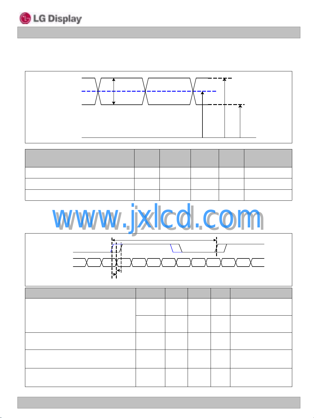
LVDS +
LVDS -
0V
V
CM
# |VID| = |(LVDS +) – (LVDS -)|
# VCM= {(LVDS +) + ( LVDS -)}/2
|VID|
V
IN_MAXVIN_MIN
LVDS Data
t
SKEW
LVDS Clock
T
clk
t
SKEW (Fclk
= 1/T
clk
)
1) 85MHz > Fclk ≥ 65MHz : -400 ~ +400
2) 65MHz > Fclk ≥ 25MHz : -600 ~ +600
3-3. LVDS Signal Timing Specifications
3-3-1. DC Specification
LP156WH9
Liquid Crystal Display
Description
LVDS Common mode Voltage
LVDS Input Voltage Range
3-3-2. AC Specification
www.jxlcd.com
www.jxlcd.com
LVDS Clock to Data Skew Margin
Symbo
l
CM
IN
SKEW
SKEW
NotesUnitMaxMin
-mV600100|VID|LVDS Differential Voltage
-V1.80.6V
-V2.10.3V
NotesUnitMaxMinSymbolDescription
ps+ 400 400-t
600-
ps+ 600t
85MHz > Fclk ≥
65MHz
65MHz > Fclk ≥
25MHz
LVDS Clock to Clock Skew Margin (Even
to Odd)
Maximum deviation
of input clock frequency during SSC
Maximum modulation frequency
of input clock during SSC
Ver. 0.0 Mar. 8, 2011
SKEW_EO
DEV
MOD
- 1/7
+ 1/7t
T
clk
%± 3-F
KHz200-F
-
-
-
9 / 32
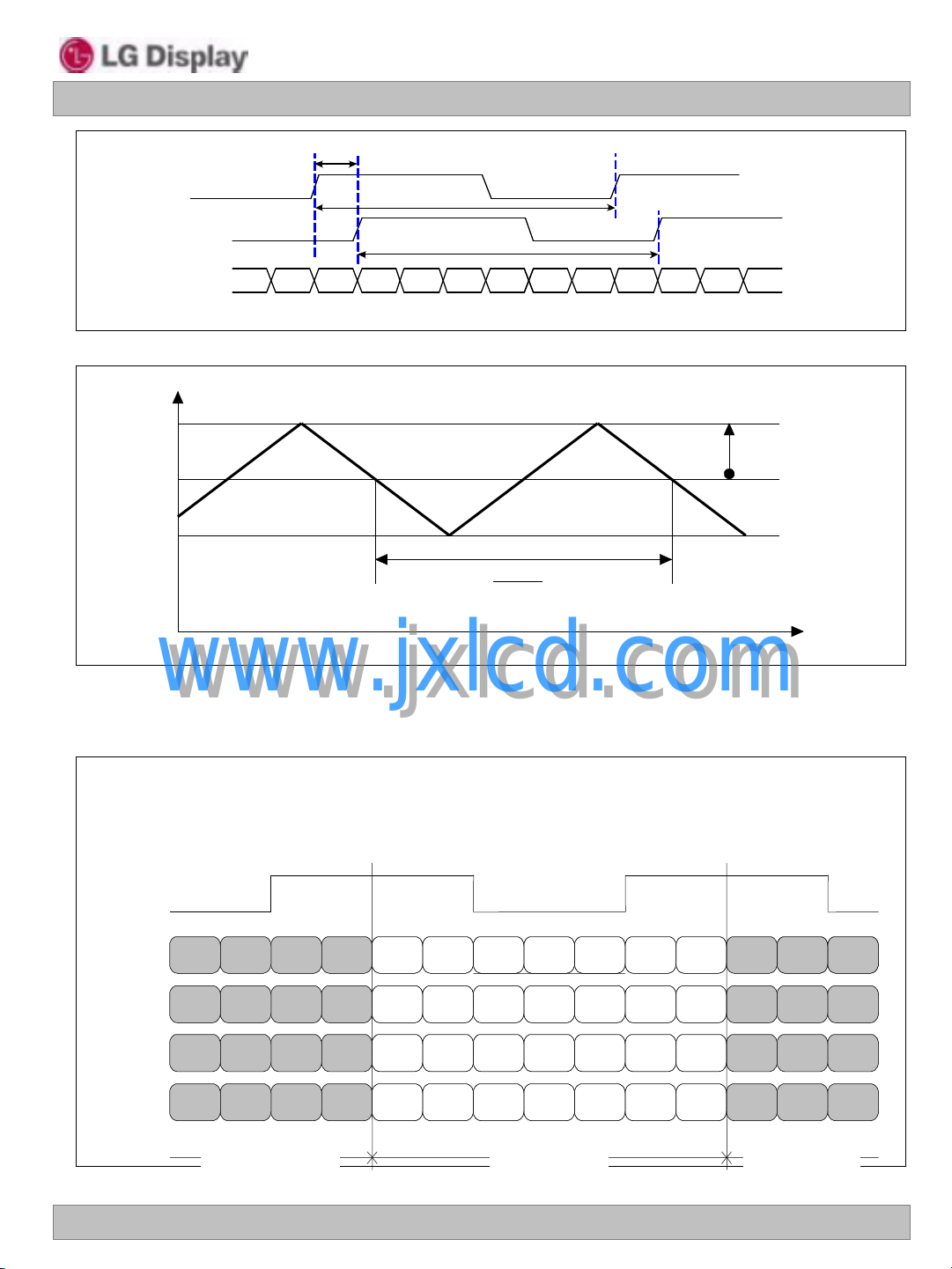
LVDS Even Data
LVDS Odd Clock
LVDS Even Clock
t
SKEW_EO
T
clk
T
clk
Freq.
F
max
F
center
F
min
Product Specification
< Clock skew margin between channel >
LP156WH9
Liquid Crystal Display
F
* F
center
DEV
www.jxlcd.com
www.jxlcd.com
3-3-3. Data Format
1) LVDS 1 Port
RCLK+
RA+/-
RB+/-
RC+/-
R3 R2
G4 G3
B5 B4
R1 R0
G2 G1
B3 B2
1
F
MOD
< Spread Spectrum >
G0 R5 R4 R3 R2 R1 R0
B1 B0 G5 G4 G3 G2 G1
DE VSYNC HSYNC B5 B4 B3 B2
Time
G0
B1
DE
VSYNC HSYNC
R5 R4
B0 G5
Ver. 0.0 Mar. 8, 2011
RD+/-
G7 G6
Previous (N-1)th Cycle Next(N+1)th Cycle
R7 R6
X B7 B6 G7 G6 R7 R6
Current (Nth) Cycle
< LVDS Data Format >
X
B7 B6
10 / 32
 Loading...