

LP156WH2
Liquid Crystal Display
Product Specification
SPECIFICATION
FOR
APPROVAL
)
(
(
Preliminary Specification
)
Final Specification
◆
15.6” HD TFT LCDTitle
DellCustomer
MODEL
*When you obtain standard approval,
www.jxlcd.com
www.jxlcd.com
SIGNATUREAPPROVED BY
/
/
/
please use the above model name without suffix
APPROVED BY
APPROVED BY
H. S. Kim / S.Manager
REVIEWED BY
REVIEWED BY
S. R. Kim / Manager
PREPARED BY
PREPARED BY
J. P. Lee / Engineer
B. I. Park / Engineer
LG Display Co., Ltd.SUPPLIER
LP156WH2*MODEL
TPB1Suffix
SIGNATURE
SIGNATURE
Please return 1 copy for your confirmation with
your signature and comments.
Ver. 1.0 Jan. 26, 2010
Products Engineering Dept.
LG Display Co., Ltd
1 / 32
Product Specification
Contents
LP156WH2
Liquid Crystal Display
ITEMNo
COVER
CONTENTS
RECORD OF REVISIONS
1
2
3
4
GENERAL DESCRIPTION
ABSOLUTE MAXIMUM RATINGS
ELECTRICAL SPECIFICATIONS
ELECTRICAL CHARACTREISTICS
3-1
INTERFACE CONNECTIONS
3-2
eDP SIGNAL TIMING SPECIFICATION
3-3
SIGNAL TIMING SPECIFICATIONS
3-4
SIGNAL TIMING WAVEFORMS
3-5
COLOR INPUT DATA REFERNECE
3-6
www.jxlcd.com
www.jxlcd.com
POWER SEQUENCE
3-7
OPTICAL SFECIFICATIONS
Page
1
2
3
4
5
6
8
9
10
10
11
12
13-15
5
Ver. 1.0 Jan. 26, 2010
MECHANICAL CHARACTERISTICS
RELIABLITY6
INTERNATIONAL STANDARDS7
SAFETY7-1
EMC7-2
Environment7-3
PACKING8
DESIGNATION OF LOT MARK8-1
PACKING FORM8-2
PRECAUTIONS9
APPENDIX. Enhanced Extended Display Identification Data A
16-19
23
24
24
24
25
26~27
28-29
30-32
2 / 32
Product Specification
RECORD OF REVISIONS
LP156WH2
Liquid Crystal Display
DescriptionPageRevision DateRevision No
First Draft (Preliminary Specification)AllJun. 30, 20090.0
Add PPID Label Revision Code19
Update the Electrical Characteristics.6
Update the Timing Table (Dclk 72.3Mhz → 72.0Mhz : WWAN)10
Update the Label Drawing18-19
Update the LCM Drawing21-22
Add the Packing Information26-27
Update the EDID Data (Checksum: 3C→49)30-32
www.jxlcd.com
www.jxlcd.com
EDID
ver
0.0
0.1Updated Rear view (Label)18Aug. 17, 20090.1
0.2Update the EDID Data28-30Nov. 27. 20090.2
1.0Final Specification-Jan. 26. 20101.0
Ver. 1.0 Jan. 26, 2010
3 / 32
LP156WH2
Liquid Crystal Display
Product Specification
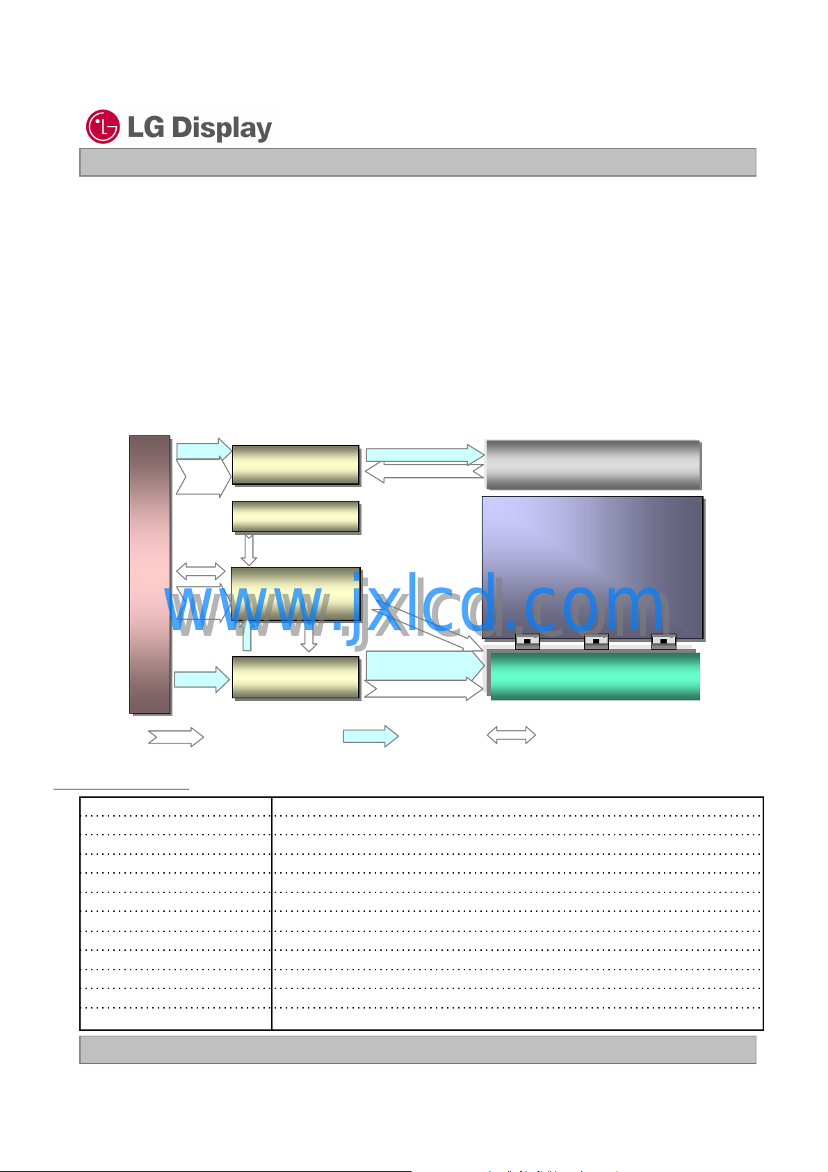
1. General Description
The LP156WH2 is a Color Active Matrix Liquid Crystal Display with an integral LED backlight system. The
matrix employs a-Si Thin Film Transistor as the active element. It is a transmissive type display operating in
the normally white mode. This TFT-LCD has 15.6 inches diagonally measured active display area with HD
resolution (1366 horizontal by 768 vertical pixel array). Each pixel is divided into Red, Green and Blue subpixels or dots which are arranged in vertical stripes. Gray scale or the brightness of the sub-pixel color is
determined with a 6-bit gray scale signal for each dot, thus, presenting a palette of more than 262,144
colors. The LP156WH2 has been designed to apply the interface method that enables low power, high
speed, low EMI. The LP156WH2 is intended to support applications where thin thickness, low power are
critical factors and graphic displays are important. In combination with the vertical arrangement of the subpixels, the LP156WH2 characteristics provide an excellent flat display for office automation products such
as Notebook PC.
User connector
30
Pin
www.jxlcd.com
www.jxlcd.com
General Features
VLED
LED_EN
PWM /
SMBUS
eDP
VCC
Control & Data Power
LED Driver
LED Driver
Block
Block
EEPROM Block
EEPROM Block
for Tcon & EDID
for Tcon & EDID
Timing Control
Timing Control
(Tcon) Block
(Tcon) Block
DVCC
Power
Block
TCLKs
Power
Block
15.6 inches diagonal Active Screen Size
359.3(H, Typ.) × 209.5(V, Typ.) × 5.5(D, Max.) mmOutline Dimension
0.252mm X 0.252mmPixel Pitch
1366 horiz. by 768 vert. Pixels RGB strip arrangementPixel Format
6-bit, 262,144 colorsColor Depth
220 cd/m2(Typ., 5 points)Luminance, White
Total 4.9 W(Typ.) Logic : 1.4 W (Typ.@ Mosaic), B/L : 3.5W (Typ. With LED Driver )Power Consumption
470g (Max.)Weight
Transmissive mode, normally whiteDisplay Operating Mode
Anti-Glare treatment of the front Polarizer Surface Treatment
YesRoHS Compliance
Yes for allBFR / PVC / As Free
VGH, VGL, GMA
VOUT_LED
FB1~4
M
i
n
i
-
L
V
D
S
DVCC, AVDD
GIP CLKs, DSC
1
768
LED Backlight Ass’y
1366
TFT-LCD Panel
(HD, GIP, TN)
Source Driver
(Bottom Bent)
EDID signal & Power
Ver. 1.0 Jan. 26, 2010
4 / 32
LP156WH2
Liquid Crystal Display
Product Specification
2. Absolute Maximum Ratings
The following are maximum values which, if exceeded, may cause faulty operation or damage to the unit.
Table 1. ABSOLUTE MAXIMUM RATINGS
60
Values
90% 80%
MaxMin
60
40
20
10
%
%
%
%
Parameter Notes
Power Input Voltage
Operating Temperature
Storage Temperature
Operating Ambient Humidity
Storage Humidity
Note : 1. Temperature and relative humidity range are shown in the figure below.
Wet bulb temperature should be 39°CMax, and no condensation of water.
www.jxlcd.com
www.jxlcd.com
Wet Bulb
Temperature [℃℃℃℃]
20
10
0
Symbol
OP
ST
OP
ST
50
40
30
Units
Humidity[(%)RH]
Storage
Operation
at 25 ± 5°CVdc4.0-0.3VCC
1°C500T
1°C60-20H
1%RH9010H
1%RH9010H
-20
Ver. 1.0 Jan. 26, 2010
10
20 30 40 50
Dry Bulb Temperature [℃℃℃℃]
60 70 800
5 / 32
LP156WH2
Liquid Crystal Display
Product Specification
3. Electrical Specifications
3-1. Electrical Characteristics
The LP156WH2 requires two power inputs. The first logic is employed to power the LCD electronics and to
drive the TFT array and liquid crystal. The second backlight is the input about LED BL with LED Driver.
Table 2. ELECTRICAL CHARACTERISTICS
Values
NotesUnit
10%0.2-0
11Hz1000-200F
12Hrs--15,000
LOGIC :
Power Supply Input Voltage
MosaicPower Supply Input Current
Power Consumption
Power Supply Inrush Current
LVDS Impedance
BACKLIGHT : ( with LED Driver)
LED Power Input Voltage
LED Power Input Current
LED Power Consumption
LED Power Inrush Current
PWM Jitter
PWM Impedance
PWM Frequency
PWM High Level Voltage
PWM Low Level Voltage
SMBus CLK & Data High Level Voltage
SMBus CLK & Data Low Level Voltage
SMBus CLK Frequency
SMBus Data Setup time
SMBus Data Hold time
SMBus CLK/Data Rising time
SMBus CLK/Data Falling time
Life Time
www.jxlcd.com
www.jxlcd.com
SymbolParameter
LED_P
PWM_H
PWM_L
CC
CC
CC
CC_P
LVDS
LED
LED
LED
-
PWM
PWM
SBL_H
SBL_L
SB_C
SBD_S
SBD_H
SB_R
SB_F
-
MaxTypMin
11010090Z
Ω
kΩ604020Z
V5.3-3.0V
V0.3-0V
V5.3-3.0V
V0.3-0V
kHz605550F
us--250T
us--300T
us3--T
us3--T
1V3.63.33.0V
2mA485420-I
2W1.61.4-P
3mA2000--I
4
5V21.012.07.0V
6mA315290-I
7W3.83.5-P
8mA2000--I
9%100-5-PWM Duty Ratio
Ver. 1.0 Jan. 26, 2010
6 / 32
Liquid Crystal Display
Product Specification
Note)
1. The measuring position is the connector of LCM and the test conditions are under 25℃, fv = 60Hz,
Black pattern.
2. The specified Icc current and power consumption are under
the Vcc = 3.3V , 25℃, fv = 60Hz condition and Mosaic pattern.
3. This Spec. is the max load condition for the cable impedance designing.
4. The below figures are the measuring Vcc condition and the Vcc control block LGD used.
The Vcc condition is same as the minimum of T1 at Power on sequence.
LP156WH2
Rising time
Vcc
0V
www.jxlcd.com
5. This impedance value is needed for proper display and measured form LVDS Tx to the mating connector.
6. The measuring position is the connector of LCM and the test conditions are under 25℃.
7. The current and power consumption with LED Driver are under the Vled = 12.0V , 25℃, Dimming of
Max luminance and White pattern with the normal frame frequency operated(60Hz).
8. The below figures are the measuring Vled condition
and the Vled control block LGD used.
VLED control block is same with Vcc control block.
90%
10%
0.5ms
www.jxlcd.com
3.3V
Rising time
V
LED
0V
10%
12.0V
90%
0.5ms
9. The operation of LED Driver below minimum dimming ratio may cause flickering or reliability issue.
10. If Jitter of PWM is bigger than maximum, it may induce flickering.
11. This Spec. is not effective at 100% dimming ratio as an exception because it has DC level equivalent
to 0Hz. In spite of acceptable range as defined, the PWM Frequency should be fixed and stable for
more consistent brightness control at any specific level desired.
12. The life time is determined as the sum of the continuous operation time at which brightness of LCD at the
typical LED current is 50% compare to that of minimum value specified in table 7 under general user
condition.
Ver. 1.0 Jan. 26, 2010
7 / 32
LP156WH2
Liquid Crystal Display
Product Specification
3-2. Interface Connections
This LCD employs two interface connections, a 30 pin connector is used for the module electronics interface
and the other connector is used for the integral backlight system.
Table 3. MODULE CONNECTOR PIN CONFIGURATION (CN1)
NotesDescriptionSymbolPin
1
2
3
4
5
6
7
8
9
10
11
12
VCC
13
VCC
www.jxlcd.com
14
15
16
17
18
19
20
21
GND LED Backlight Ground
22
LED_EN (NC)
23
PWM
24
25
26
VLED
27
VLED
28
VLED
29
VLED
30
www.jxlcd.com
Dell’s Test Loop to 30pinPAID
High Speed (Main Link) GroundGND
Complement Signal-Lane 1 ( No Connection )Lane1_N
True Signal-Main Lane 1 ( No Connection )Lane1_p
High Speed (Main Link) GroundGND
Complement Signal-Lane 0Lane0_N
True Signal-Main Lane 0Lane0_p
High Speed (Main Link) GroundGND
True Signal-Auxiliary ChannelAUX_P
Complement Signal-Auxiliary ChannelAUX_N
High Speed (Main Link) GroundGND
LCD Logic and driver power (3.3V Typ.)
LCD Logic and driver power (3.3V Typ.)
LCD Panel Self Test EnableBIST
GroundGND
GroundGND
HPD signal pinHPD
LED Backlight GroundGND
LED Backlight GroundGND
LED Backlight GroundGND
NO Connect
System PWM Signal input for dimming
Backlight Control ClkSMBUS_CLK
Backlight Control DataSMBUS_DATA
LED Backlight Power (7.0V-21V)
LED Backlight Power (7.0V-21V)
LED Backlight Power (7.0V-21V)
LED Backlight Power (7.0V-21V)
Dell’s Test Loop to 1pinPAID
[Interface Chip]
1. LCD :
IDT, VPP1420 (LCD Controller
Including eDP Receiver.
2. System : TBD or equivalent
* Pin to Pin compatible with eDP
[Connector]
CABLINE-VS RECE ASS’Y, Hirose
or its compatibles
[Mating Connector]
CABLINE-VS PLUG CABLE ASS’Y or
equivalent.
[Connector pin arrangement]
30
[LCD Module Rear View]
1
Ver. 1.0 Jan. 26, 2010
8 / 32
LP156WH2
Liquid Crystal Display
Product Specification
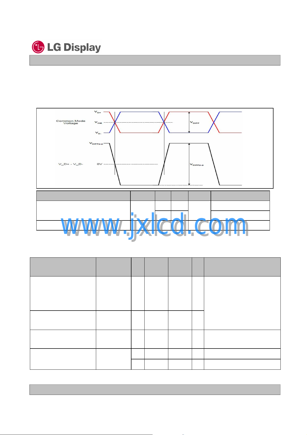
3-3. eDP Signal Timing Specifications
3-3-1. DC Specification
The VESA Display Port related AC specification is compliant with the VESA Display Port Standard v1.1a.
NotesUnitMaxMinSymbolDescription
Differential peak-to-peak Input voltage
Rx DC common mode voltage
www.jxlcd.com
www.jxlcd.com
VDIFF p-p
CM
-120
mV
For high bit rate
For reduced bit rate-40
-V2.00V
3-3-2. AC Specification
The VESA Display Port related AC specification is compliant with the VESA Display Port Standard v1.1a.
Unit Interval for high bit rate
(2.7Gbps/lane)
Unit Interval for high bit rate
(1.62Gbps/lane)
Lane-to-Lane skew
V Rx-SKEWINTER_PAIR
Typ
370
-
617
-
-
Range is nominal ±350ppm.
ps-UI_High_Rate
DisplayPort Link Rx does not
require local crystal for link
clock generation
ps-UI_Low_Rate
-
ps5200-
NotesUnitMaxMinSymbolDescription
Lane intra-pair skew
Ver. 1.0 Jan. 26, 2010
V Rx-SKEWINTRA_PAIR
-
For high bit rate
ps100-
For reduced bit rateps300--
9 / 32

LP156WH2
Liquid Crystal Display
Product Specification
3-4. Signal Timing Specifications
This is the signal timing required at the input of the User connector. All of the interface signal timing should be
satisfied with the following specifications and specifications of eDP Tx/Rx for its proper operation.
Table 4. TIMING TABLE
NoteUnitMaxTypMinSymbolITEM
FrequencyDCLK
Period
Hsync
Vsync
Data
Enable
3-5. Signal Timing Waveforms
Width
Width-Active
Period
Width
Width-Active
Horizontal back porch
Horizontal front porch
Vertical back porch
Vertical front porch
www.jxlcd.com
www.jxlcd.com
Data Enable, Hsync, Vsync
t
DCLK
CLK
0.5 Vcc
CLK
t
HP
WH
WHA
VP
WV
WVA
HBP
HFP
VBP
t
VFP
High: 0.7VCC
Low: 0.3VCC
MHz-72.0-f
158615201470
403223t
136613661366t
801790779t
852t
768768768t
1247472t
48488t
20148t
531
tCLK
tHP
tCLK
tHP
Condition : VCC =3.3V
t
Hsync
t
WH
t
HBP
HP
t
WHA
Data Enable
t
VP
t
WV
Vsync
t
VBP
t
WVA
Data Enable
Ver. 1.0 Jan. 26, 2010
t
HFP
t
VFP
10 / 32
 Loading...