

LG LP156WF6-SPB1 Datasheet

The information contained in this document has been carefully researched and is, to the best
of our knowledge, accurate. However, we assume no liability for any product failures or
damages, immediate or consequential, resulting from the use of the information provided
herein. Our products are not intended for use in systems in which failures of product could
result in personal injury. All trademarks mentioned herein are property of their respective
owners. All specifications are subject to change without notice.
Datasheet
LG Display
LP156WF6-SPB1
HD-10-101
(◆) Preliminary Specification
( ) Final Specification
Title 15.6” FHD TFT LCD
LP156WF6
Liquid Crystal Display
Product Specification
SPECIFICATION
FOR
APPROVAL
Customer General
MODEL
SIGNATUREAPPROVED BY
/
/
/
SUPPLIER LG Display Co., Ltd.
*MODEL LP156WF6
Suffix SPB1
*When you obtain standard approval,
please use the above model name without suffix
APPROVED BY
APPROVED BY
D. Y. Kim / S.Manager
REVIEWED BY
REVIEWED BY
C. J. Park / Manager
PREPARED BY
PREPARED BY
J. T. Kim / Engineer
C. K. Uh / Engineer
SIGNATURE
SIGNATURE
Please return 1 copy for your confirmation with
your signature and comments.
Ver. 0.1 May. 26, 2014
Products Engineering Dept.
LG Display Co., Ltd
1 / 40

LP156WF6
Liquid Crystal Display
Product Specification
Contents
RECORD OF REVISIONS…………………………………………………………………… 3
1. GENERAL DESCRIPTION……………………………………………………………… 4
2. ABSOLUTE MAXIMUM RATINGS……………………………………………………... 5
3. ELECTRICAL SPECIFICATIONS………………………………………….…………… 6
3-1. LCD ELECTRICAL CHARACTREISTICS…..…………………………………………..... 6
3-2. LED BACKLIGHT ELECTRICAL CHARACTREISTICS………………………………..... 7
3-3. INTERFACE CONNECTIONS……………………………………………………………… 8
3-4. eDP SIGNAL TIMING SPECIFICATION………………………………………………… 9
3-5. SIGNAL TIMING SPECIFICATIONS………………………………………………………. 13
3-6. SIGNAL TIMING WAVEFORMS…………………………………………………………… 13
3-7. COLOR INPUT DATA REFERENCE……………………………………………………… 14
3-8. POWER SEQUENCE……………………………………………………………………….. 15
4. OPTICAL SPECIFICATIONS…………………………………………………………… 16
5. MECHANICAL CHARACTERISTICS…………………………………………………. 19
6. RELIABLITY……………………………………………………………………………… 23
7. INTERNATIONAL STANDARDS………………………………………………………. 24
7-1. SAFETY…………………………………………………………………..………………...… 24
7-2. ENVIRONMENT……………………………………………………………..…………...…. 24
8. PACKING………………………………………………………………………...……….. 25
8-1. DESIGNATION OF LOT MARK………………………………………………….………… 25
8-2. PACKING FORM…………………………………………………………………..………… 25
9. PRECAUTIONS…………………………………………………………………………… 26
APPENDIX A. LGD PROPOSAL FOR SYSTEM COVER DESIGN………………...……………..……. 28
PPENDIX B. LGD PROPOSAL FOR eDP INTERFACE DESIGN GUIDE…………….………………. 34
APPENDIX C. ENHANCED EXTENDED DISPLAY IDENTIFICAION DATA….…………………….….. 38
Ver. 0.1 May. 26, 2014
2 / 40
Product Specification
Record of Revisions
LP156WF6
Liquid Crystal Display
Revision No Revision Date Page Description
0.0 Mar. 27, 2014 - Preliminary Specification -
4,6,7 Update Power Consumption
0.1 May. 26. 2014
38-40 Update EDID
EDID
version
0.1
Ver. 0.1 May. 26, 2014
3 / 40
LP156WF6
Liquid Crystal Display
Product Specification
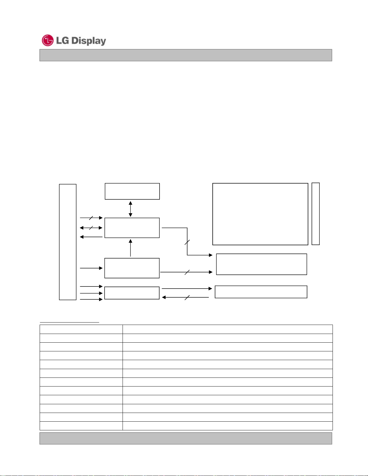
1. General Description
The LP156WF6 is a Color Active Matrix Liquid Crystal Display with an integral LED backlight system. The
matrix employs a-Si Thin Film Transistor as the active element. It is a transmissive type display operating in
the normally white mode. This TFT-LCD has 15.6 inches diagonally measured active display area with FHD
resolution (1920 horizontal by 1080 vertical pixel array). Each pixel is divided into Red, Green and Blue subpixels or dots which are arranged in vertical stripes. Gray scale or the brightness of the sub-pixel color is
determined with a 6-bit gray scale signal for each dot, thus, presenting a palette of more than 262,144
colors. The LP156WF6 has been designed to apply the interface method that enables low power, high
speed, low EMI. The LP156WF6 is intended to support applications where thin thickness, low power are
critical factors and graphic displays are important. In combination with the vertical arrangement of the subpixels, the LP156WF6 characteristics provide an excellent flat display for office automation products such as
Notebook PC.
EEPROM
1
for EDID & T-Con
TFT-LCD Panel
User connector
Main Link
AUX
HPD
I2C
Timing
Controller
Data Signal,
Gate Signal
TFT-LCD Panel
(1920 x RGB x 1080)
(1920 x RGB x 1080)
1080
DVCC
30
Pin
VCC
VLED
LED_EN
PWM
Power Block
LED Driver
DVCC, AVDD,
Vcom, Gamma
VOUT_LED
LED Cathode
Source Driver
LED Backlight
General Features
Active Screen Size 15.6 inches diagonal
Outline Dimension
Pixel Pitch 0.17925 mm X 0.17925 mm
Pixel Format 1920 horiz. By 1080 vert. Pixels RGB strip arrangement
Color Depth 6-bit, 262,144 colors
Luminance, White 300 cd/m2(Typ.)
Power Consumption Total 5.4W (Typ.) Logic : 1.1W (Typ. @ Mosaic), B/L : 4.3W (Typ.)
Weight 350g (Max.) / 340g(Typ.)
Display Operating Mode Normally Black
Surface Treatment Anti-glare treatment of the front Polarizer
RoHS Compliance Yes
BFR / PVC / As Free Yes for all
359.5(H, Typ.) × 223.80(V, Typ.) × 3.2(D, Max.) [mm](with Bracket & PCB Board)
19201
Gate Driver
Ver. 0.1 May. 26, 2014
4 / 40
LP156WF6
Liquid Crystal Display
Product Specification
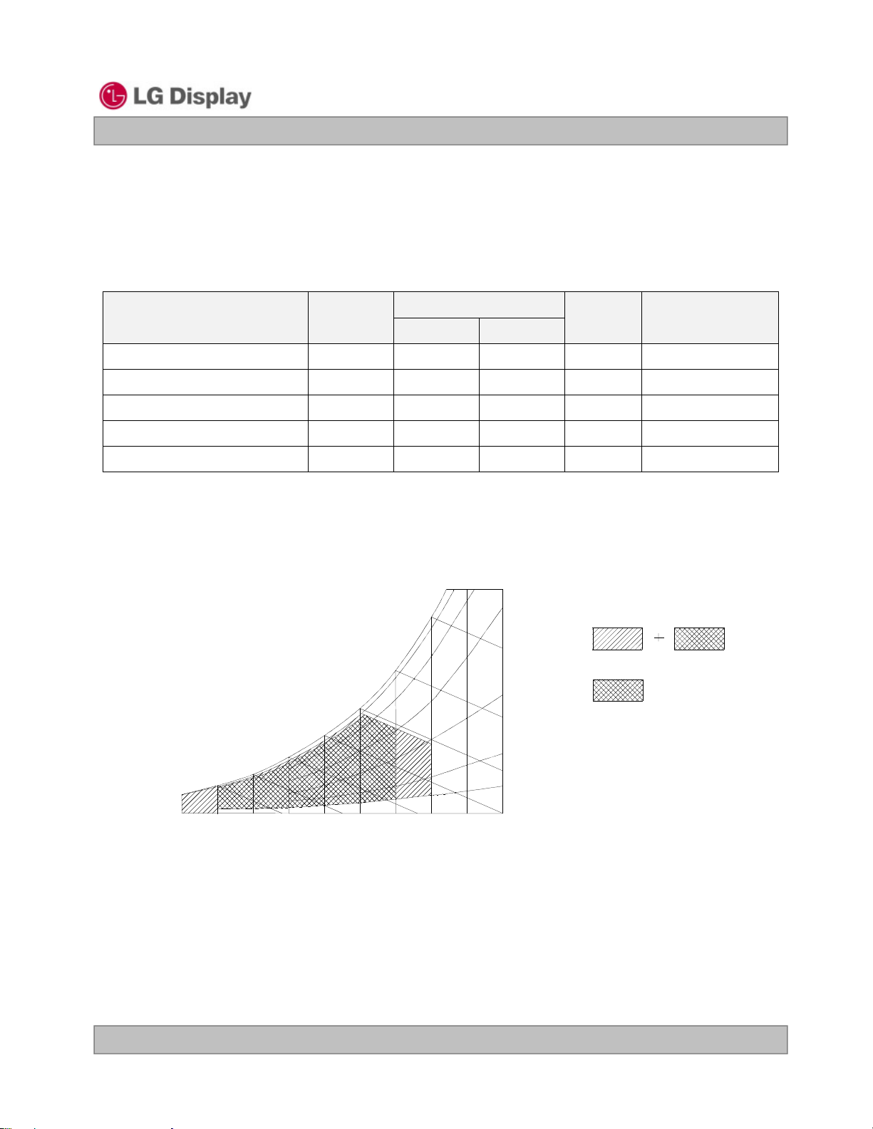
2. Absolute Maximum Ratings
The following are maximum values which, if exceeded, may cause faulty operation or damage to the unit.
Table 1. ABSOLUTE MAXIMUM RATINGS
Parameter Symbol
Units Notes
Min Max
Values
Power Input Voltage
Operating Temperature
Storage Temperature
Operating Ambient Humidity
Storage Humidity
VCC -0.3 4.0 V
TOP 0 50 ° C 1
HST -20 60 ° C 1
HOP 10 90 %RH 1
HST 10 90 %RH 1
Note : 1. Temperature and relative humidity range are shown in the figure below.
Wet bulb temperature should be 39°C Max, and no condensation of water.
Note : 2. Storage Condition is guaranteed under packing condition.
90% 80%
60%
Humidity[(%)RH]
Storage
40%
Operation
20%
10%
Wet Bulb
Temperature [℃℃℃℃]
20
10
0
60
50
40
30
DC
at 25 ± 2°C
-20
10
20 30 40 50
60 70 800
Dry Bulb Temperature [℃℃℃℃]
Ver. 0.1 May. 26, 2014
5 / 40
3. Electrical Specifications
3-1. LCD Electrical Characteristics
Table 2. LCD ELECTRICAL CHARACTERISTICS
LP156WF6
Liquid Crystal Display
Product Specification
Parameter Symbol
Unit Notes
Min Typ Max
Power Supply Input Voltage VCC 3.0 3.3 3.6 V 1
Values
Permissive Power Supply Input Ripple
Power Supply
Input Current
Mosaic ICC
Red (Max. Rating) I
VCCrp
CC_MAX
Power Consumption PCC
- - 100 mV
- 348 402
- 423 486
-
1.1 1.3
mA
mA
p-p
W
Power Supply Inrush Current ICC_P - - 1.5 A 3
Differential Impedance ZLVDS 90 100 110 Ω
Note)
1. The measuring position is the connector of LCM and the test conditions are under 25℃, fv = 60Hz
2. The specified ICCcurrent and power consumption are under the VCC= 3.3V , 25℃, fv = 60Hz condition
and Mosaic pattern.
2
3. The VCCrising time is same as the minimum of T1 at Power on sequence.
Rising time
V
CC
0V
10%
90%
3.3V
0.5ms
Ver. 0.1 May. 26, 2014
6 / 40
Product Specification
3-2. LED Backlight Electrical Characteristics
Table 3. LED B/L ELECTRICAL CHARACTERISTICS
LP156WF6
Liquid Crystal Display
Parameter Symbol
Unit Notes
Min Typ Max
LED Power Input Voltage VLED 5.5 12.0 21.0 V 1
Values
LED Power Input Current ILED -
LED Power Consumption PLED -
359 371
4.3 4.4
mA
W
LED Power Inrush Current ILED_P - - 1.5 A 3
PWM Duty Ratio 5 - 100 % 4
PWM Jitter 0 - 0.2 % 5
PWM Frequency FPWM 200 - 1000 Hz 6
PWM
High Level Voltage V
Low Level Voltage V
PWM_H
PWM_L
3.0 - 5.3 V
0 - 0.3 V
High Voltage VLED_EN_H 3.0 - 5.3 V
LED_EN
Low Voltage VLED_EN_L 0 - 0.3 V
Life Time 12,000 - - Hrs 7
Note)
1. The measuring position is the connector of LCM and the test conditions are under 25℃.
2. The current and power consumption with LED Driver are under the V
= 12.0V , 25℃, PWM Duty 100%
LED
and White pattern with the normal frame frequency operated(60Hz).
3. The V
rising time is same as the minimum of T13 at Power on sequence.
LED
12.0V
Rising time
90%
VLED
2
0V
10%
0.5ms
4. The operation of LED Driver below minimum dimming ratio may cause flickering or reliability issue.
5. If Jitter of PWM is bigger than maximum, it may induce flickering.
6. This Spec. is not effective at 100% dimming ratio as an exception because it has DC level equivalent to 0Hz.
In spite of acceptable range as defined, the PWM Frequency should be fixed and stable for more consistent
brightness control at any specific level desired.
7. The life time is determined as the time at which brightness of LCD is 50% compare to that of minimum
value specified in table 7. under general user condition.
Ver. 0.1 May. 26, 2014
7 / 40
Liquid Crystal Display
Product Specification
3-3. Interface Connections
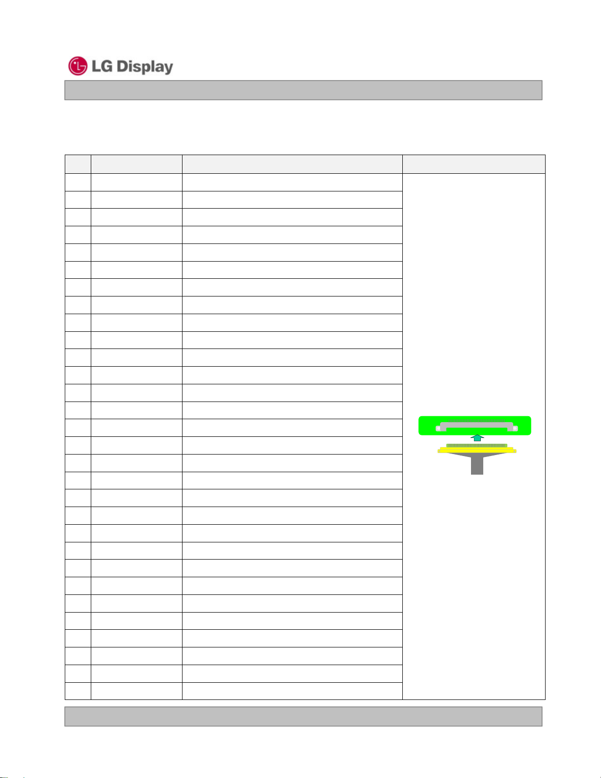
Table 4. MODULE CONNECTOR PIN CONFIGURATION (CN1)
Pin Symbol Description Notes
1 NC Reserved Reserved for LCD manufacturer’s use
2 GND High Speed Ground
3 Lane1_N Complement Signal Link Lane 1
4 Lane1_P True Signal Link Lane 1
5 GND High Speed Ground
6 Lane0_N Complement Signal Link Lane 0
7 Lane0_P True Signal Link Lane 0
8 GND High Speed Ground
LP156WF6
9 AUX_CH_P True Signal Auxiliary Channel
10 AUX_CH_N Complement Signal Auxiliary Channel
11 GND High Speed Ground
12 VCC LCD logic and driver power
13 VCC LCD logic and driver power
14 LCD Self Test or NC LCD Panel Self Test Enable (Optional)
15 GND LCD logic and driver ground
16 GND LCD logic and driver ground
17 HPD HPD signal pin
18 BL_GND LED Backlight ground
19 BL_GND LED Backlight ground
20 BL_GND LED Backlight ground
21 BL_GND LED Backlight ground
22 BL ENABLE LED Backlight control on/off control
23 BL PWM System PWM signal input for dimming
24 NC Reserved Reserved for LCD manufacture’s use
25 NC Reserved Reserved for LCD manufacture’s use
[Connector]
HRS KN38B-30S-0.5H
or JAE, equivalent
[Connector pin arrangement]
Pin 30 Pin 1
[LGD P-Vcom using information]
1. Pin for P-Vcom : #24, #25
2. P-Vcom Address : 0101000x
26 VLED LED Backlight power (12V Typical)
27 VLED LED Backlight power (12V Typical)
28 VLED LED Backlight power (12V Typical)
29 VLED LED Backlight power (12V Typical)
30 NC Reserved Reserved for LCD manufacture’s use
Ver. 0.1 May. 26, 2014
8 / 40
Product Specification
3-3. eDP Signal Timing Specifications
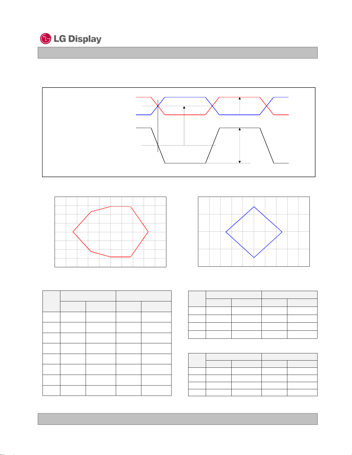
3-3-1. Definition of Differential Voltage
V
V
V
DIFF
0 V
D+
V
CM
D-
Common Mode Voltage
VCM= (VD++ VD-) / 2
V
= VD+- V
DIFF
V
= (2* max | VD+- VD-|)
DIFFp-p
D-
[ Definition of Differential Voltage ]
3-3-2. Main Link EYE Diagram
LP156WF6
Liquid Crystal Display
V
DIFF
V
CM
V
DIFFp-p
2
3 4
Volts
1
5
8
67
0.0 0.1 0.2 0.3 0.4 0.5 0.6 0.7 0.8 0.9 1.0
UI
[ EYE Mask at Source Connector Pins ] [ EYE Mask at Sink Connector Pins ]
Point
1 0.127 0.000 0.210 0.000
2 0.291 0.160 0.355 0.140
3 0.500 0.200 0.500 0.175
4 0.709 0.200 0.645 0.175
5 0.873 0.000 0.790 0.000
6 0.709 -0.200 0.645 -0.175
7 0.500 -0.200 0.500 -0.175
8 0.291 -0.160 0.355 -0.140
Reduced Bit Rate High Bit Rate
Time(UI) Voltage(V) Time(UI) Voltage(V)
[ EYE Mask Vertices at Source Connector Pins ]
2
Volts
1
3
4
0.0 0.1 0.2 0.3 0.4 0.5 0.6 0.7 0.8 0.9 1.0
UI
Point
Reduced Bit Rate High Bit Rate
Time(UI) Voltage(V) Time(UI) Voltage(V)
1 0.375 0.000 0.246 0.000
2 0.500 0.023 0.500 0.075
3 0.625 0.000 0.755 0.000
4 0.500 -0.023 0.500 -0.075
[ EYE Mask Vertices at Sink Connector Pins ]
Point
1 0.270 0.000 0.246 0.000
2 0.500 0.068 0.500 0.075
3 0.731 0.000 0.755 0.000
4 0.500 -0.068 0.500 -0.075
Reduced Bit Rate High Bit Rate
Time(UI) Voltage(V) Time(UI) Voltage(V)
[ EYE Mask Vertices at embedded DP Sink Connector Pins ]
Ver. 0.1 May. 26, 2014
9 / 40
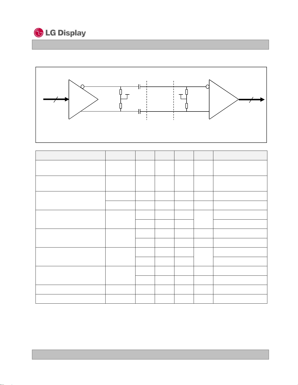
3-3-3. eDP Main Link Signal
8
T
X
Product Specification
Vbias
50Ω
50Ω
Tx
C_ML
C_ML
ML_N
ML_P
Vbias
Rx
50Ω
50Ω
LP156WF6
Liquid Crystal Display
8
R
X
Parameter Symbol Min Typ Max Unit Notes
Unit Interval for high bit rate
(2.7Gbps / lane)
Unit Interval for reduced bit rate
(1.62Gbps / lane)
Link Clock Down Spreading
Differential peak-to-peak voltage
at Source side connector
EYE width
at Source side connector
Differential peak-to-peak voltage
at Sink side connector
Source
Connector
Sink
Connector
[ Main Link Differential Pair ]
UI_HBR - 370 - ps
UI_RBR - 617 - ps
Amplitude 0 - 0.5 %
Frequency 30 33 kHz
V
TX-DIFFp-p
T
TX-EYE-CONN
V
RX-DIFFp-p
350 - -
mV
400 - - For RBR(1.62Gbps)
0.58 - - UI For HBR(2.7Gbps)
0.75 - - UI For RBR(1.62Gbps)
150 - -
mV
136 - - For RBR(1.62Gbps)
For HBR(2.7Gbps)
For HBR(2.7Gbps)
EYE width
at Sink side connector
T
RX-EYE-CONN
Rx DC common mode voltage V
AC Coupling Capacitor C
SOURCE_ML
RX CM
0.51 - - UI For HBR(2.7Gbps)
0.46 - - UI For RBR(1.62Gbps)
0 - 1.0 V
75 200 nF Source side
Note)
1. Termination resistor is typically integrated into the transmitter and receiver implementations.
2. AC Coupling Capacitor is not placed at the sink side.
3. In cabled embedded system, it is recommended the system designer ensure that EYE width and voltage are met
at the sink side connector pins.
Ver. 0.1 May. 26, 2014
10 / 40
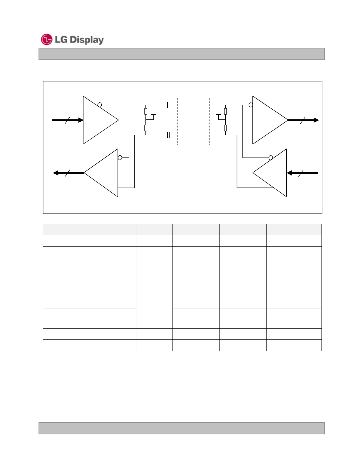
3-3-4. eDP AUX Channel Signal
8 8
50Ω
AUX Ch.
T
X
50Ω
Product Specification
Aux_Ch_N
Vbias
C_Aux
Tx
C_Aux
Aux_Ch_P
Vbias
Rx
50Ω
50Ω
Liquid Crystal Display
AUX Ch.
R
X
LP156WF6
Source
Connector
8 8
AUX Ch.
R
X
Sink
Connector
AUX Ch.
T
X
[ Recommended eDP AUX Channel Differential Pair ]
Parameter Symbol Min Typ Max Unit Notes
AUX Unit Interval UI 0.4 - 0.6 us
AUX Jitter at Tx IC Package Pins
T
AUX Jitter at Rx IC Package Pins - - 0.05 UI Equal to 30ns
jitter
AUX Peak-to-peak voltage
at Connector Pins of Receiving
AUX Peak-to-peak voltage
at Connector Pins of Transmitting
V
AUX-DIFFp-p
AUX EYE width
at Connector Pins of Tx and Rx
- - 0.04 UI Equal to 24ns
0.39 - 1.38 V
0.36 - 1.36 V
0.98 - - UI
AUX DC common mode voltage V
AUX AC Coupling Capacitor C
Note)
1. Termination resistor is typically integrated into the transmitter and receiver implementations.
2. AC Coupling Capacitor is not placed at the sink side.
3. V
AUX-DIFFp-p
Ver. 0.1 May. 26, 2014
= 2*|V
AUXP-VAUXN
|
AUX-CM
SOURCE-AUX
0 - 1.0 V
75 200 nF Source side
11 / 40
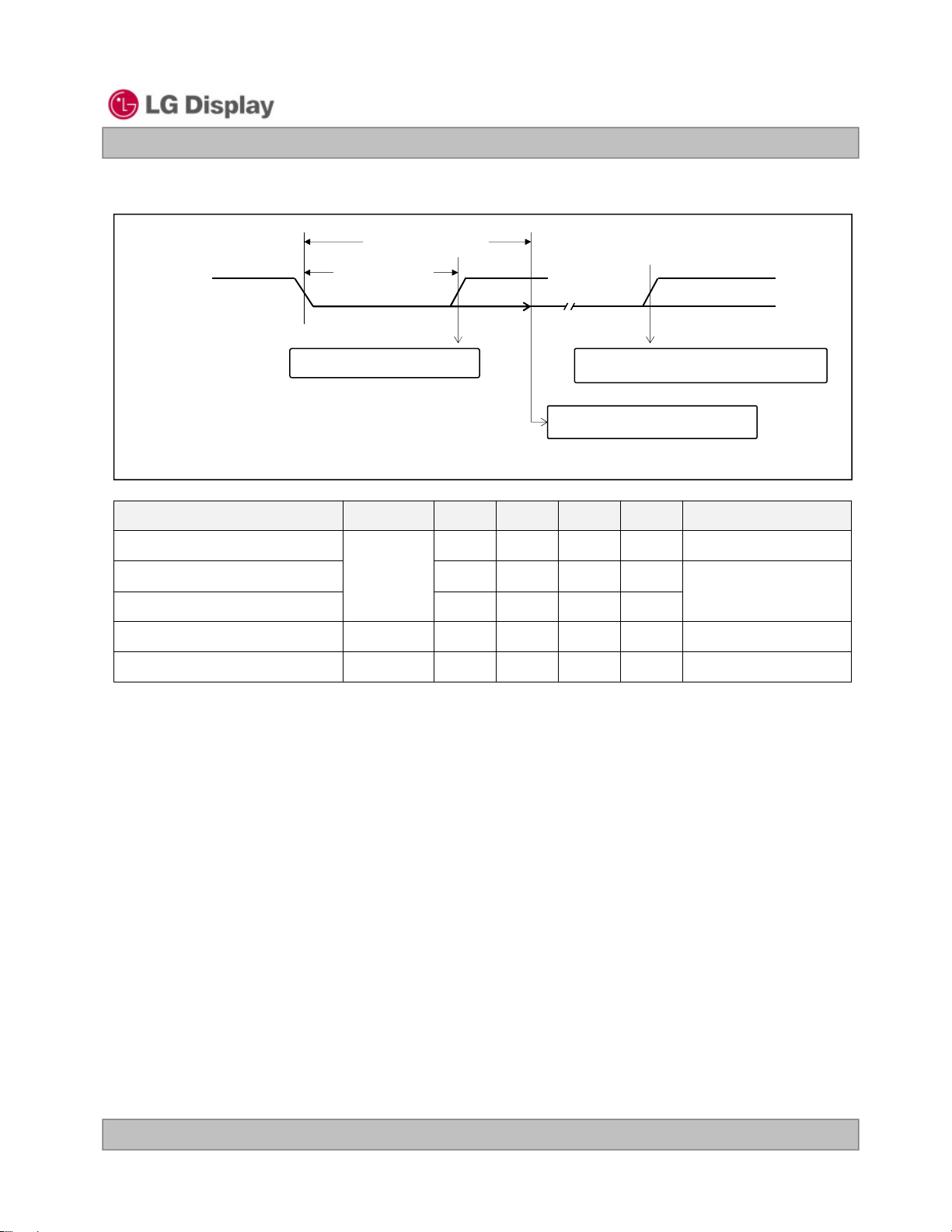
3-3-5. eDP HPD Signal
HPD
LP156WF6
Liquid Crystal Display
Product Specification
HPD_TimeOut (2ms)
HPD_IRQ Pulse
(0.5 ~ 1.0ms)
Case1 : HPD IRQ Event
Case3 : Hot Plug / Re-plug Event
Case2 : Hot Unplug Event
[ HPD Events ]
Parameter Symbol Min Typ Max Unit Notes
HPD Voltage
Hot Plug Detection Threshold 2.0 - - V
HPD
2.25 - 3.6 V Sink side Driving
Source side Detecting
Hot Unplug Detection Threshold - - 0.8 V
HPD_IRQ Pulse Width HPD_IRQ 0.5 - 1.0 ms
HPD_TimeOut 2.0 - - ms HPD Unplug Event
Note)
1. HPD IRQ : Sink device wants to notify the Source device that Sink’s status has changed so it toggles HPD line,
forcing the Source device to read its Link / Sink Receiver DPCD field via the AUX-CH
2. HPD Unplug : The Sink device is no longer attached to the Source device and the Source device may then disable its
Main Link as a power saving mode
3. Plug / Re-plug : The Sink device is now attached to the Source device, forcing the Source device to read its Receiver
capabilities and Link / Sink status Receiver DPCD fields via the AUX-CH
Ver. 0.1 May. 26, 2014
12 / 40
 Loading...