

Product Specification
SPECIFICATION
LP154WP2
Liquid Crystal Display
FOR
APPROVAL
)
(
(
Preliminary Specification
)
Final Specification●
www.jxlcd.com
www.jxlcd.com
15.4” WXGA+ TFT LCDTitle
DELLBUYER
-MODEL
*When you obtain standard approval,
please use the above model name without suffix
LG.Philips LCD Co., Ltd.SUPPLIER
LP154WP2*MODEL
TLC1Suffix
DATESIGNATURE
/
/
/
Please return 1 copy for your confirmation with
your signature and comments.
Ver. 1.0 10, MAY, 2008
APPROVED BY DATE
J. L. Ma / G. Manager
REVIEWED BY
W. Y. Park / Manager
PREPARED BY
S. S. Han / Engineer
K. M. Lee / Engineer
Product Engineering Dept.
LG. Philips LCD Co., Ltd
1 / 33
Product Specification
Contents
LP154WP2
Liquid Crystal Display
ITEMNo
COVER
CONTENTS
RECORD OF REVISIONS
GENERAL DESCRIPTION1
ABSOLUTE MAXIMUM RATINGS2
ELECTRICAL SPECIFICATIONS3
ELECTRICAL CHARACTREISTICS 3-1
INTERFACE CONNECTIONS 3-2
LVDS SIGNAL TIMING SPECIFICATIONS 3-3
SIGNAL TIMING SPECIFICATIONS 3-4
SIGNAL TIMING WAVEFORMS 3-5
www.jxlcd.com
www.jxlcd.com
COLOR INPUT DATA REFERNECE 3-6
POWER SEQUENCE 3-7
OPTICAL SFECIFICATIONS4
Page
1
2
3
4
5
6
7
9
12
12
13
14
15
MECHANICAL CHARACTERISTICS5
RELIABLITY6
INTERNATIONAL STANDARDS7
SAFETY 7-1
EMC 7-2
PACKING8
DESIGNATION OF LOT MARK 8-1
PACKING FORM 8-2
PRECAUTIONS9
APPENDIX A. Enhanced Extended Display Identification DataA
Ver. 1.0 10, MAY, 2008
22
26
27
27
28
28
29
31
2 / 33
Product Specification
RECORD OF REVISIONS
LP154WP2
Liquid Crystal Display
DescriptionPageRevision DateRevision No
First Draft-14. Nov. 2007.0.0
Add Mechanical drawing, update label information17~1926. Feb. 2008.0.1
Change label information & Size18~193. Mar. 2008.0.2
Update the Power Consumption4, 68. May. 2008.0.3
Add the LVDS signal timing spec.9~11
12, 14
www.jxlcd.com
www.jxlcd.com
Update the signal timing spec. and Power sequence
Update the optical spec. and gamma scale spec.15, 16
Add the appendix – LPL proposal for system cover design19~21
Add the EDID Data (Check sum : 95)31~33
Update Mechanical drawing (Change the S/Cover drawing)2410. May. 2008.1.0
EDID ver
-
-
-
1.0
1.0
1.0
1.0
1.0
1.0
1.0
Ver. 1.0 10, MAY, 2008
3 / 33
LP154WP2
Liquid Crystal Display
Product Specification
1. General Description
The LP154WP2 is a Color Active Matrix Liquid Crystal Display with an integral LED backlight system. The
matrix employs a-Si Thin Film Transistor as the active element. It is a transmissive type display operating in
the normally white mode. This TFT-LCD has 15.4 inches diagonally measured active display area with
WXGA resolution(1440 horizontal by 900 vertical pixel array). Each pixel is divided into Red, Green and Blue
sub-pixels or dots which are arranged in vertical stripes. Gray scale or the brightness of the sub-pixel color is
determined with a 6-bit gray scale signal for each dot, thus, presenting a palette of more than 262,144
colors.
The LP154WP2 has been designed to apply the interface method that enables low power, high speed, low
EMI.
The LP154WP2 is intended to support applications where thin thickness, low power are critical factors and
graphic displays are important. In combination with the vertical arrangement of the sub-pixels, the
LP154WP2 characteristics provide an excellent flat display for office automation products such as Notebook
PC.
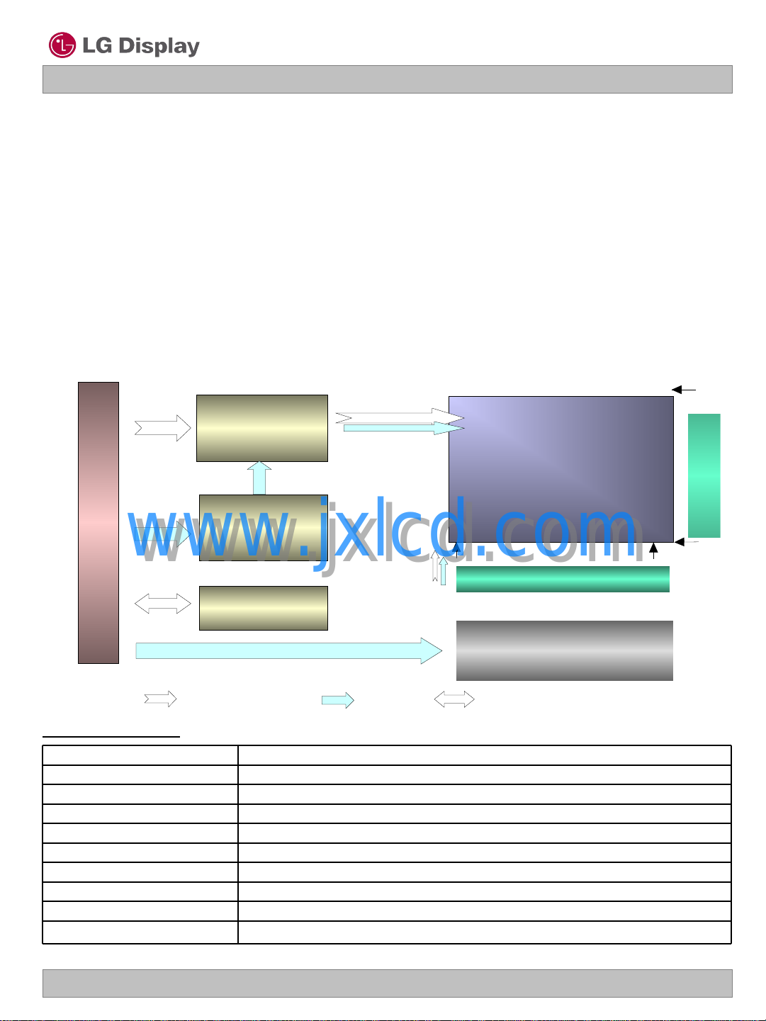
CN1 User connector 50 Pin
www.jxlcd.com
www.jxlcd.com
General Features
LVDS &
Timing
Control
Block
POWE
R
BLOCK
EDID
BLOCK
Control & Data Power EDID signal & Power
15.4 inches diagonal Active Screen Size
344.0 (H, typ.) × 222.0 (V, typ.) × 6.1(D, max.) mmOutline Dimension
0.2301 mm × 0.2301 mm Pixel Pitch
1440 horiz. by 900 vert. Pixels RGB strip arrangementPixel Format
6-bit, 262,144 colorsColor Depth
300 cd/m2(Typ.) , 5 pointLuminance, White
Total 4.6 Watt(Typ.) @ LCM circuit 1.0Watt(Typ.), B/L 3.6Watt(Typ.)Power Consumption
460g (Max.)Weight
Transmissive mode, normally whiteDisplay Operating Mode
Hard coating(3H) Anti-Glare treatment of the front PolarizerSurface Treatment
TFT-LCD Panel
(1440 x 900)
Source Driver Circuit
LED Backlight Ass’y
10LEDs X 6 strings
(LOG_B type)
1440
1
Gate Driver
9001
Ver. 1.0 10, MAY, 2008
4 / 33
LP154WP2
Liquid Crystal Display
Product Specification
2. Absolute Maximum Ratings
The following are maximum values which, if exceeded, may cause faulty operation or damage to the unit.
Table 1. ABSOLUTE MAXIMUM RATINGS
Parameter Notes
Power Input Voltage
Operating Temperature
Storage Temperature
Operating Ambient Humidity
Storage Humidity
Note : 1. Temperature and relative humidity range are shown in the figure below.
Wet bulb temperature should be 39C Max, and no condensation of water.
www.jxlcd.com
www.jxlcd.com
Wet Bulb
Temperature [℃]
20
10
0
Symbol
60
50
40
30
Values
MaxMin
90% 80%
60%
40%
20%
10%
Units
Humidity[(%)RH]
Storage
Operation
at 25 5CVdc4.0-0.3VCC
1C500TOP
1C60-20HST
1%RH9010HOP
1%RH9010HST
-20
Ver. 1.0 10, MAY, 2008
10
20 30 40 50
Dry Bulb Temperature [℃]
60 70 800
5 / 33
LP154WP2
Liquid Crystal Display
Product Specification
3. Electrical Specifications
3-1. Electrical Characteristics
The LP154WP2 requires two power inputs. One is employed to power the LCD electronics and to drive the
TFT array and liquid crystal. The second input which powers the LED BL, is typically generated by an
LED array.
Table 2. ELECTRICAL CHARACTERISTICS
Parameter Symbol
MODULE :
Power Supply Input Current
LED BL:
Operating Current per String
Power Consumption
I
LED
CC
LED
Values
MaxTypMin
3.63.33.0VCC Power Supply Input Voltage
NotesUnit
DC
3V
1mA345300255
1Watt1.140.99-Pc Power Consumption
2Ohm11010090Zm Differential Impedance
4mA20.019.05.0I
5Watt3.903.60-P
6Hrs--10,000 Life Time
Note)
1. The specified current and power consumption are under the Vcc = 3.3V , 25℃, fv = 60Hz condition
whereas Mosaic pattern is displayed and fv is the frame frequency.
2. This impedance value is needed to proper display and measured form LVDS Tx to the mating connector.
3. The variance of the voltage is ± 10%.
4. The typical operating current is for the typical surface luminance (LWH) in optical characteristics.
I
LED
5. The LED power consumption shown above does not include power of external LED driver circuit
for typical current condition.
6. The life time is determined as the time at which brightness of LED is 50% compare to that of minimum
value specified in table 7.
www.jxlcd.com
www.jxlcd.com
is the current of each LEDs’ string, LED backlight has 6 strings on it.
Ver. 1.0 10, MAY, 2008
6 / 33
LP154WP2
Odd_Rin0- - LVDS differential data input (R0-R5, G0)
Odd_Rin0+ + LVDS differential data input (R0-R5, G0)
VSS1 Ground – Shield LVDS Ch1
Odd_Rin1- - LVDS differential data input (G1-G5, B0-B1) (odd pixels)
Odd_Rin1+ + LVDS differential data input (G1-G5, B0-B1) (odd pixels)
VSS2 Ground – Shield LVDS Ch2
Odd_Rin2- - LVDS differential data input (B2-B5, HS, VS, DE) (odd pixels)
Odd_Rin2+ + LVDS differential data input (B2-B5, HS, VS, DE) (odd pixels)
VSS3 Ground – Shield LVDS Ch3
Odd_ClkIN- - LVDS differential clock input (odd pixels)
Odd_ClkIN+ + LVDS differential clock input (odd pixels)
VSS4 Ground – Shield LVDS Ch4
Even_Rin0- - LVDS differential data input (R0-R5, G0) (even pixels)
Even_Rin0+ + LVDS differential data input (R0-R5, G0) (even pixels)
VSS5 Ground – Shield LVDS Ch5
Even_Rin1- - LVDS differential data input (G1-G5, B0-B1) (even pixels)
Even_Rin1+ + LVDS differential data input (G1-G5, B0-B1) (even pixels)
VSS6 Ground – Shield LVDS Ch6
Even_Rin2- - LVDS differential data input (B2-B5, HS, VS, DE) (even pixels)
Even_Rin2+ + LVDS differential data input (B2-B5, HS, VS, DE) (even pixels)
VSS7 Ground – Shield LVDS Ch7
Even_ClkIN- - LVDS differential clock input (even pixels)
Even_ClkIN+ + LVDS differential clock input (even pixels)
Test Loop Test Loop (only to pin 1)
Liquid Crystal Display
Product Specification
3-2. Interface Connections
This LCD employs two interface connections, a 50 pin connector is used for the module electronics interface
and the other connector is used for the integral backlight system.
The electronics interface connector is a model FI-VHP50S-A-HF11manufactured by JAE.
Table 3. MODULE CONNECTOR PIN CONFIGURATION (CN1)
www.jxlcd.com
www.jxlcd.com
Ver. 1.0 10, MAY, 2008
7 / 33
Pin No. 31~50
Pin Signal Description
31 CONNTEST connector test (this pin is connected to pin 20 only) See note 1.
32 VDD Logic Power 3.3V (Panal logic, BL logic)
33 VDD Logic Power 3.3V (Panal logic, BL logic)
34
TEST
(BIST_EN)
Panel Self Test
35 +5V_ALW SMBUS 5V power
36 VSS Ground (Panal logic, BL logic)
37 VSS Ground (Panal logic, BL logic)
38 PWM_BL PWM brightness control
39 VBL_ Ground (LED logic)
40 VBL_ Ground (LED logic)
41 VBL_ Ground (LED logic)
42 VBL_ Ground (LED logic)
43 NC no connect
44 VBL+ 7V ~ 20V LED power
45 VBL+ 7V ~ 20V LED power
46 VBL+ 7V ~ 20V LED power
47 VBL+ 7V ~ 20V LED power
48 SMB_DATA SMBus Data
49 SMB_CLK SMBus Clock
50 CONNTEST connector test (this pin is connected to pin 1 only) See note 1.
LP154WP2
Liquid Crystal Display
Product Specification
www.jxlcd.com
www.jxlcd.com
Connector Typ
JAE, FI-VHP50S-A-HF11 (50pin)
Ver. 1.0 10, MAY, 2008
8 / 33
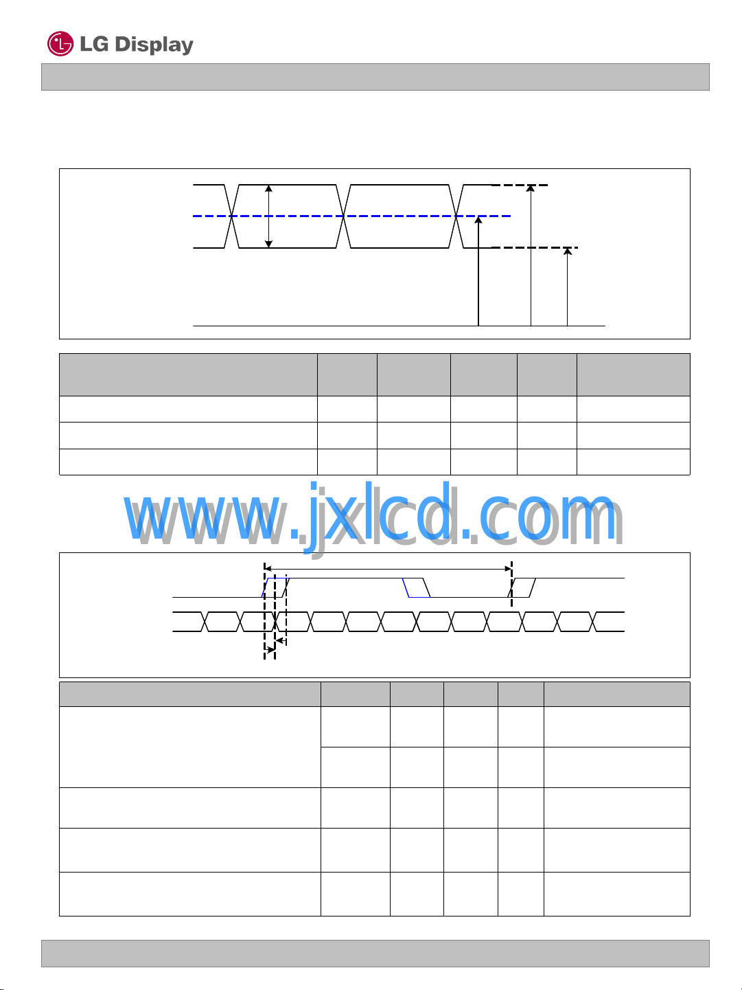
Product Specification
LVDS +
LVDS -
0V
V
CM
# |VID| = |(LVDS +) – (LVDS -)|
# VCM= {(LVDS +) + ( LVDS -)}/2
|VID|
V
IN_MAXVIN_MIN
LVDS Data
t
SKEW
LVDS Clock
T
clk
t
SKEW (Fclk
= 1/T
clk
)
1) 85MHz > Fclk ≥ 65MHz : -400 ~ +400
2) 65MHz > Fclk ≥ 25MHz : -600 ~ +600
3-3. LVDS Signal Timing Specifications
3-3-1. DC Specification
LP154WP2
Liquid Crystal Display
Description
LVDS Common mode Voltage
LVDS Input Voltage Range
3-3-2. AC Specification
www.jxlcd.com
www.jxlcd.com
LVDS Clock to Data Skew Margin
Symbo
l
CM
IN
SKEW
SKEW
NotesUnitMaxMin
-mV600100|VID|LVDS Differential Voltage
-V1.80.6V
-V2.10.3V
NotesUnitMaxMinSymbolDescription
ps+ 400 400-t
600-
ps+ 600t
85MHz > Fclk ≥
65MHz
65MHz > Fclk ≥
25MHz
LVDS Clock to Clock Skew Margin (Even
to Odd)
Maximum deviation
of input clock frequency during SSC
Maximum modulation frequency
of input clock during SSC
Ver. 1.0 10, MAY, 2008
SKEW_EO
DEV
MOD
- 1/7
+ 1/7t
T
clk
%± 3-F
KHz200-F
-
-
-
9 / 33
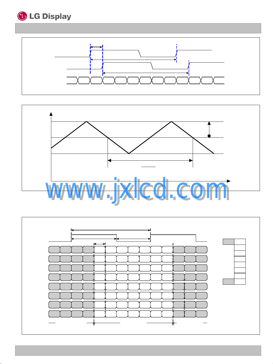
LVDS Even Data
LVDS Odd Clock
LVDS Even Clock
t
SKEW_EO
T
clk
T
clk
OG0 OR5 OR4 OR3 OR2 OR1 OR0
OB1 OB0 OG5 OG4 OG3 OG2 OG1
DE VSYNC HSYNC OB5 OB4 OB3 OB2
X OB7 OB6 OG7 OG6 OR7 OR6
Current(Nth) CyclePrevious(N-1)th Cycle Next(N+1)th Cycle
RCLK +
RXinO0 +/-
Tclk * 4/7 Tclk * 3/7
Tclk
Tclk * 1/7
MSB R7
R6
R5
R4
R3
R2
R1
R0LSB
EG0 ER5 ER4 ER3 ER2 ER1 ER0
EB1 EB0 EG5 EG4 EG3 EG2 EG1
DE
VSYNC HSYNC
EB5 EB4 EB3 EB2
X EB7 EB6 EG7 EG6 ER7 ER6
* ODD = 1st Pixel
EVEN = 2nd Pixel
RXinO1 +/-
RXinO2 +/-
RXinO3 +/-
RXinE0 +/-
RXinE1 +/-
RXinE2 +/-
RXinE3 +/-
OR3 OR2 OR1 OR0
OG4 OG3 OG2 OG1
OB5 OB4 OB3 OB2
OG7 OG6 OR7 OR6
ER3 ER2 ER1 ER0
EG4 EG3 EG2 EG1
EB5 EB4 EB3 EB2
EG7 EG6 ER7 ER6
OG0 OR5 OR4
OB1 OB0 OG5
DE VSYNC HSYNC
X OB7 OB6
EG0 ER5 ER4
EB1 EB0 EG5
DE
VSYNC HSYNC
X EB7 EB6
Freq.
F
max
F
center
F
min
Product Specification
< Clock skew margin between channel >
LP154WP2
Liquid Crystal Display
F
* F
center
DEV
3-3-3. Data Format
1) LVDS 2 Port
Ver. 1.0 10, MAY, 2008
www.jxlcd.com
www.jxlcd.com
< Spread Spectrum >
< LVDS Data Format >
1
F
MOD
Time
10 / 33
 Loading...