

LG LP-154WE2-TLA4 Service manual
Product Specification
SPECIFICATION
LP154WE2
Liquid Crystal Display
FOR
APPROVAL
)
(
(
Preliminary Specification
)
Final Specification
◆
MODEL
www.jxlcd.com
15.4” WSXGA+ TFT LCDTitle
GeneralCustomer
*When you obtain standard approval,
www.jxlcd.com
please use the above model name without suffix
LG.Philips LCD Co., Ltd.SUPPLIER
LP154WE2*MODEL
TLA4Suffix
SIGNATUREAPPROVED BY
/
/
/
Please return 1 copy for your confirmation with
your signature and comments.
Ver. 1.0
Feb.20, 2008
APPROVED BY
S.C. Yoon S.Manager
REVIEWED BY
Y. S. Ha Manager
PREPARED BY
S. H. Jang Engineer
Products Engineering Dept.
LG. Philips LCD Co., Ltd
SIGNATURE
1 / 31
Product Specification
Contents
LP154WE2
Liquid Crystal Display
ITEMNo
COVER
CONTENTS
RECORD OF REVISIONS
GENERAL DESCRIPTION1
ABSOLUTE MAXIMUM RATINGS2
ELECTRICAL SPECIFICATIONS3
ELECTRICAL CHARACTREISTICS 3-1
INTERFACE CONNECTIONS 3-2
LVDS SIGNAL TIMING SPECIFICATIONS 3-3
SIGNAL TIMING SPECCIFICATIONS 3-4
SIGNAL TIMING WAVEFORMS 3-5
www.jxlcd.com
www.jxlcd.com
COLOR INPUT DATA REFERNECE 3-6
POWER SEQUENCE 3-7
OPTICAL SFECIFICATIONS4
Page
1
2
3
4
5
6
8
9
11
11
12
13
14
Ver. 1.0
MECHANICAL CHARACTERISTICS5
RELIABLITY6
INTERNATIONAL STANDARDS7
SAFETY 7-1
EMC 7-2
PACKING8
DESIGNATION OF LOT MARK 8-1
PACKING FORM 8-2
PRECAUTIONS9
APPENDIX. Enhanced Extended Display Identification Data A
Feb.20, 2008
17
24
25
25
26
26
27
29
2 / 31
Product Specification
RECORD OF REVISIONS
LP154WE2
Liquid Crystal Display
DescriptionPageRevision DateRevision No
First Draft (Preliminary Specification)-Feb.20. 20080.0
www.jxlcd.com
www.jxlcd.com
EDID
ver
0.0
0.1
Ver. 1.0
Feb.20, 2008
3 / 31
LP154WE2
Liquid Crystal Display
Product Specification
1. General Description
The LP154WE2 is a Color Active Matrix Liquid Crystal Display with an integral Cold Cathode Fluorescent
Lamp (CCFL) backlight system. The matrix employs a-Si Thin Film Transistor as the active element. It is a
transmissive type display operating in the normally white mode. This TFT-LCD has 15.4 inches diagonally
measured active display area with WSXGA+ resolution(1680 vertical by 1050 horizontal pixel array). Each
pixel is divided into Red, Green and Blue sub-pixels or dots which are arranged in vertical stripes. Gray scale
or the brightness of the sub-pixel color is determined with a 6-bit gray scale signal for each dot, thus,
presenting a palette of more than 262,144 colors.
The LP154WE2 has been designed to apply the interface method that enables low power, high speed, low
EMI. Flat Link must be used as a LVDS(Low Voltage Differential Signaling) chip.
The LP154WE2 is intended to support applications where thin thickness, low power are critical factors and
graphic displays are important. In combination with the vertical arrangement of the sub-pixels, the
LP154WE2 characteristics provide an excellent flat display for office automation products such as Notebook
PC.
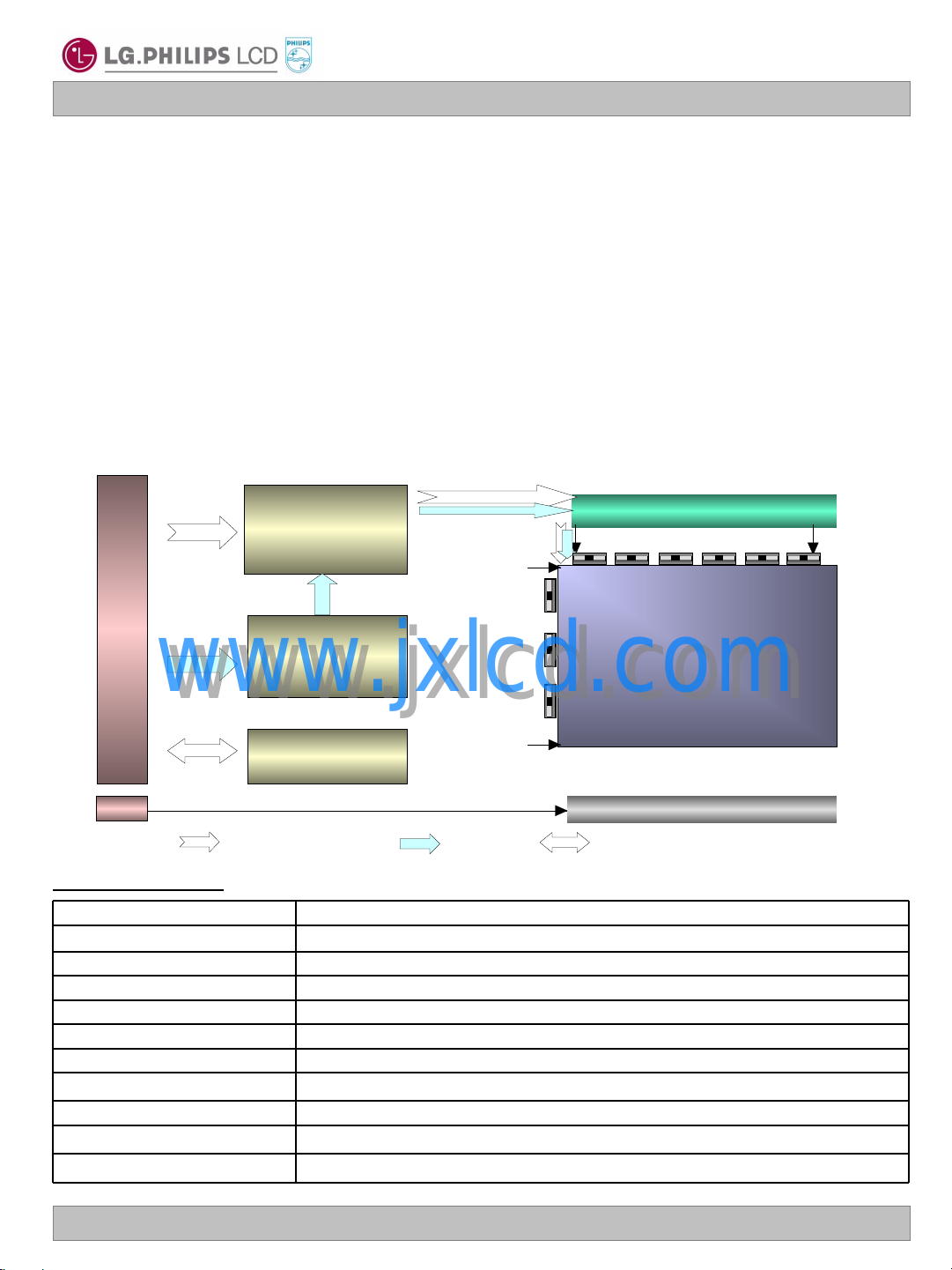
CN1 User connector 30 Pin
www.jxlcd.com
www.jxlcd.com
CN
General Features
Outline Dimension
LVDS &
Timing
Control
Block
POWER
BLOCK
EDID
BLOCK
Control & Data Power EDID signal & Power
15.4 inches diagonal Active Screen Size
344.0(H, typ) × 222.0(V, typ) × 6.5(D) mm[Max.]
0.19725 mm x 0.19725mmPixel Pitch
1680 horiz. By 1050 vert. Pixels RGB stripes arrangementPixel Format
6-bit, 262,144 colorsColor Depth
200 cd/m2(Typ.5 point)Luminance, White
5.66 (Typ.) (Mosaic Pattern@ LCM circuit 1.52.W(Typ.) ,B/L input 4.14 W (Typ.)Power Consumption
590g(Max.)Weight
Transmissive mode, normally whiteDisplay Operating Mode
Anti-glare treatment of the front polarizer (HAZE 44%)Surface Treatment
YesRoHS Comply
(LOG_B type)
1050
1
Source Driver Circuit
1
TFT-LCD Panel
(1680 x 1050)
Backlight Ass’y
1680
Ver. 1.0
Feb.20, 2008
4 / 31
LP154WE2
Liquid Crystal Display
Product Specification
2. Absolute Maximum Ratings
The following are maximum values which, if exceeded, may cause faulty operation or damage to the unit.
Table 1. ABSOLUTE MAXIMUM RATINGS
Parameter Notes
Power Input Voltage
Operating Temperature
Storage Temperature
Operating Ambient Humidity
Storage Humidity
Note : 1. Temperature and relative humidity range are shown in the figure below.
Wet bulb temperature should be 39C Max, and no condensation of water.
www.jxlcd.com
www.jxlcd.com
Wet Bulb
Temperature [℃]
20
10
0
Symbol
60
50
40
30
Values
MaxMin
90% 80%
60%
40%
20%
10%
Units
Humidity[(%)RH]
Storage
Operation
at 25 5CVdc4.0-0.3VCC
1C500TOP
1C60-20HST
1%RH9010HOP
1%RH9010HST
Ver. 1.0
-20
10
20 30 40 50
Dry Bulb Temperature [℃]
Feb.20, 2008
60 70 800
5 / 31
LP154WE2
Liquid Crystal Display
Product Specification
3. Electrical Specifications
3-1. Electrical Characteristics
The LP154WE2 requires two power inputs. One is employed to power the LCD electronics and to drive the
TFT array and liquid crystal. The second input which powers the CCFL, is typically generated by an
inverter. The inverter is an external unit to the LCD.
Table 2. ELECTRICAL CHARACTERISTICS
Parameter Symbol
MODULE :
Power Supply Input Current
LAMP :
Operating Voltage
Operating Current
Power Consumption
Operating Frequency
www.jxlcd.com
www.jxlcd.com
I
CC
Mosaic
Black
Window XP
Bliss Pattern
BL
BL
BL
BL
Values
DC
RMS
RMS
NotesUnit
1mA530460390
1Watt1.761.52-Pc Power Consumption
2Ohm11010090Zm Differential Impedance
3mA
4Min3--Ts Discharge Stabilization Time
5Hrs--12,000 Life Time
MaxTypMin
3.63.33.0VCC Power Supply Input Voltage
820690660V
7.06.03.0I
4.624.14-P
V
mA640550460
mA540470400
V
kHz806045f
Established Starting Voltage
at 25℃
at 0 ℃
Note)
1. The specified current and power consumption are under the Vcc = 3.3V , 25℃, fv = 60Hz condition
whereas Mosaic pattern is displayed and fv is the frame frequency.
2. This impedance value is needed to proper display and measured form LVDS Tx to the mating connector.
3. The typical operating current is for the typical surface luminance (LWH) in optical characteristics.
4. Define the brightness of the lamp after being lighted for 5 minutes as 100%, Ts is the time required for
the brightness of the center of the lamp to be not less than 95%.
5. The life time is determined as the time at which brightness of lamp is 50% compare to that of initial value
at the typical lamp current.
Ver. 1.0
Vs
Feb.20, 2008
1200
1380
V
RMS
V
RMS
6 / 31
LP154WE2
Liquid Crystal Display
Product Specification
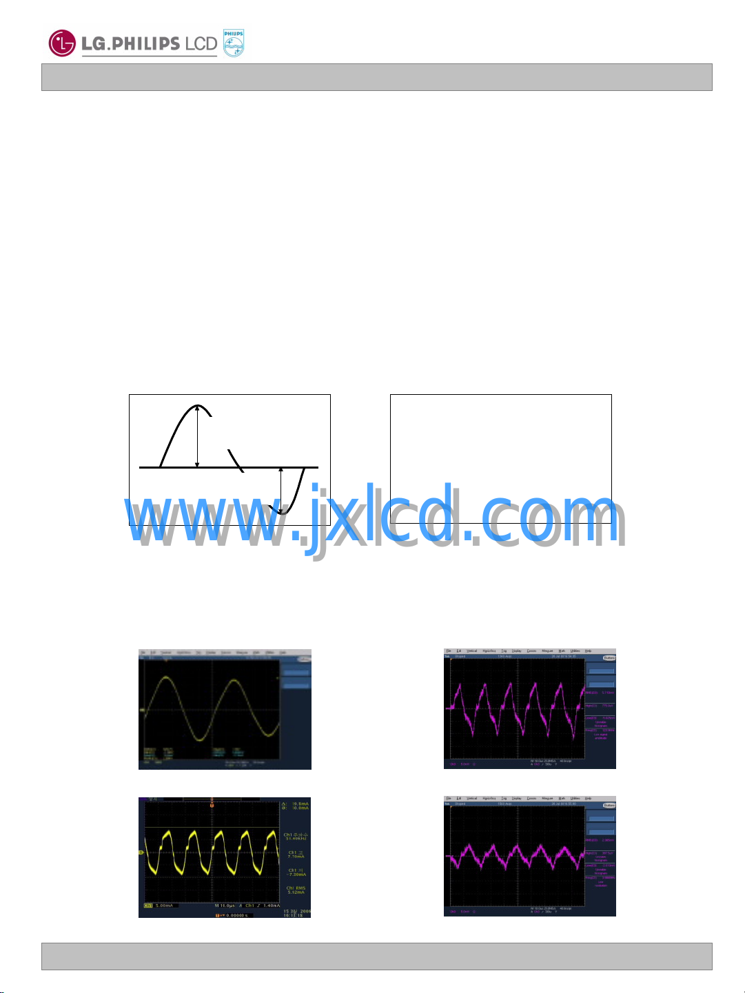
Note)
6. The output of the inverter must have symmetrical(negative and positive) voltage waveform and
symmetrical current waveform.(Asymmetrical ratio is less than 10%) Please do not use the inverter
which has asymmetrical voltage and asymmetrical current and spike wave.
Lamp frequency may produce interface with horizontal synchronous frequency and as a result this may
cause beat on the display. Therefore lamp frequency shall be as away possible from the
horizontal synchronous frequency and from its harmonics in order to prevent interference.
7. It is defined the brightness of the lamp after being lighted for 5 minutes as 100%.
TS is the time required for the brightness of the center of the lamp to be not less than 95%.
8. The lamp power consumption shown above does not include loss of external inverter.
The applied lamp current is a typical one.
9. Requirements for a system inverter design, which is intended to have a better display performance, a
better power efficiency and a more reliable lamp, are following.
It shall help increase the lamp lifetime and reduce leakage current.
a. The asymmetry rate of the inverter waveform should be less than 10%.
b. The distortion rate of the waveform should be within √2 ±10%.
* Inverter output waveform had better be more similar to ideal sine wave.
* Asymmetry rate:
I p
| I p – I –p | / I
* 100%
rms
10. Inverter open voltage must be more than lamp voltage for more than 1 second for start-up.
Otherwise, the lamps may not be turned on.
※ Do not attach a conducting tape to lamp connecting wire.
If the lamp wire attach to a conducting tape, TFT-LCD Module has a low luminance and the inverter
has abnormal action. Because leakage current is occurred between lamp wire and conducting tape.
Ex of current wave)
www.jxlcd.com
www.jxlcd.com
Normal current wave - Standard
I -p
* Distortion rate
I p (or I –p) / I
Abnormal current wave - Bad
rms
Ver. 1.0
Abnormal current wave - Bad
Feb.20, 2008
Abnormal current wave - Bad
7 / 31
LP154WE2
Liquid Crystal Display
Product Specification
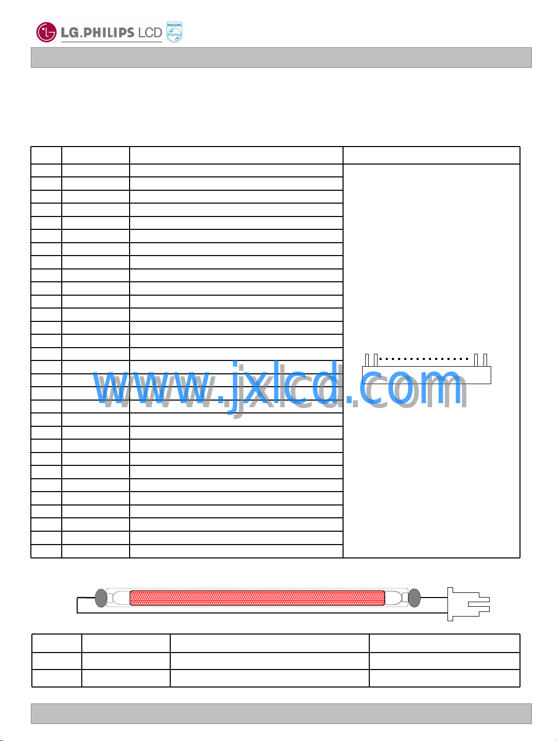
3-2. Interface Connections
This LCD employs two interface connections, a 30 pin connector is used for the module electronics interface
and the other connector is used for the integral backlight system.
The electronics interface connector is a model GT101-30S-HR11 manufactured by LSC.
Table 3. MODULE CONNECTOR PIN CONFIGURATION (CN1)
NotesDescriptionSymbolPin
GroundGND1
Power Supply, 3.3V Typ.VCC2
Power Supply, 3.3V Typ.VCC3
DDC 3.3V powerV EEDID4
Reserved for supplier test pointNC5
DDC ClockClk EEDID6
DDC DataDATA EEDID7
Negative LVDS differential data inputODD_R
0-8
IN
Positive LVDS differential data inputODD_RIN0+9
GroundGND10
Negative LVDS differential data inputODD_RIN 1- 11
Positive LVDS differential data inputODD_RIN 1+12
GroundGND13
Negative LVDS differential data inputODD_RIN 2-14
Positive LVDS differential data inputODD_RIN 2+15
GroundGND16
Negative LVDS differential clock inputODD_CLKIN-17
www.jxlcd.com
www.jxlcd.com
EVEN_RIN0+ Positive LVDS differential data input21
Positive LVDS differential clock inputODD_CLKIN+18
GroundGND19
Negative LVDS differential data inputEVEN_R
0-20
IN
GroundGND22
Negative LVDS differential data inputEVEN_RIN 1- 23
Positive LVDS differential data inputEVEN_RIN 1+24
GroundGND25
Negative LVDS differential data inputEVEN_RIN 2-26
Positive LVDS differential data inputEVEN_RIN 2+27
GroundGND28
Negative LVDS differential clock inputEVEN_CLKIN-29
Positive LVDS differential clock inputEVEN_CLKIN+30
The backlight interface connector is a model BHSR-02VS-1, manufactured by JST or Compatible.
The mating connector part number is AMP1674817-2 or equivalent.
1, Interface chips
1.1 LCD : SW0610_M (LCD Controller)
including LVDS Receiver
1.2 System : THC63LVD823 or equivalent
* Pin to Pin compatible with LVDS
2. Connector
2.1 LCD :IS100-C30R-C15 ,UJU Elec.
GT101-30S-HR11,LS Cable
its compatibles
2.2 Mating : FI-X30M or equivalent.
2.3 Connector pin arrangement
30
[LCD Module Rear View]
1
PIN1
PIN2PIN2
Table 4. BACKLIGHT CONNECTOR PIN CONFIGURATION (J3)
NotesDescriptionSymbolPin
1Power supply for lamp (High voltage side)HV1
1Power supply for lamp (Low voltage side)LV2
Notes : 1. The high voltage side terminal is colored Blue and the low voltage side terminal is Black.
Ver. 1.0
Feb.20, 2008
8 / 31
Product Specification
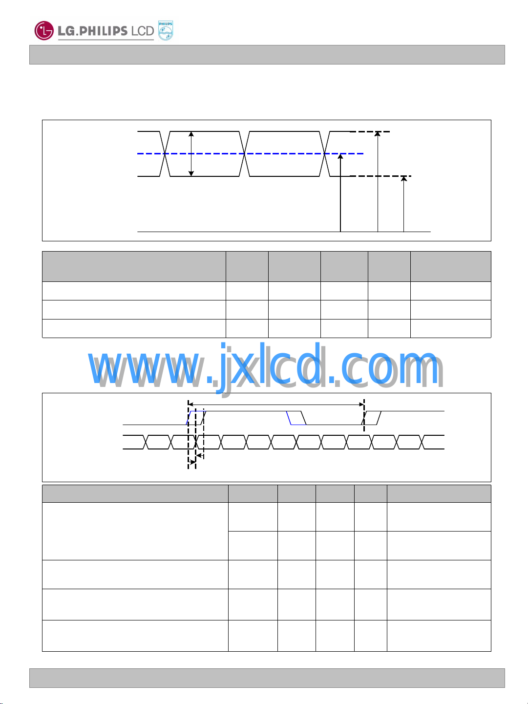
LVDS +
LVDS -
0V
V
CM
# |VID| = |(LVDS +) – (LVDS -)|
# VCM= {(LVDS +) + ( LVDS -)}/2
|VID|
V
IN_MAXVIN_MIN
LVDS Data
t
SKEW
LVDS Clock
T
clk
t
SKEW (Fclk
= 1/T
clk
)
1) 85MHz > Fclk ≥ 65MHz : -400 ~ +400
2) 65MHz > Fclk ≥ 25MHz : -600 ~ +600
3-3. LVDS Signal Timing Specifications
3-3-1. DC Specification
LP154WE2
Liquid Crystal Display
Description
LVDS Common mode Voltage
LVDS Input Voltage Range
3-3-2. AC Specification
www.jxlcd.com
www.jxlcd.com
LVDS Clock to Data Skew Margin
Symbo
l
CM
IN
SKEW
SKEW
NotesUnitMaxMin
-mV600100|VID|LVDS Differential Voltage
-V1.80.6V
-V2.10.3V
NotesUnitMaxMinSymbolDescription
ps+ 400 400-t
600-
ps+ 600t
85MHz > Fclk ≥
65MHz
65MHz > Fclk ≥
25MHz
LVDS Clock to Clock Skew Margin (Even
to Odd)
Maximum deviation
of input clock frequency during SSC
Maximum modulation frequency
of input clock during SSC
Ver. 1.0
SKEW_EO
DEV
MOD
Feb.20, 2008
- 1/7
+ 1/7t
T
clk
%± 3-F
KHz200-F
-
-
-
9 / 31
LP154WE2
Liquid Crystal Display
Product Specification
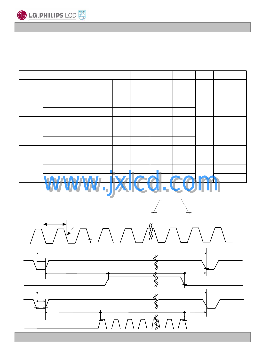
3-4. Signal Timing Specifications
This is the signal timing required at the input of the User connector. All of the interface signal timing should be
satisfied with the following specifications and specifications of LVDS Tx/Rx for its proper operation.
Table 6. TIMING TABLE
NoteUnitMaxTypMinSymbolITEM
FrequencyDCLK
Vsync
Data
Enable
3-5. Signal Timing Waveforms
Horizontal back porch
Horizontal front porch
Vertical back porch
Vertical front porch
www.jxlcd.com
www.jxlcd.com
Data Enable, Hsync, Vsync
DCLK
tCLK
0.5 Vcc
f
CLK
ThpPeriodHsync
tWH Width
t
Width-Active
WHA
tVP Period
tWV Width
t
Width-Active
WVA
t
HBP
t
HFP
t
VBP
t
VFP
High: 0.7VCC
Low: 0.3VCC
-61.0-
MHz
1288952864
-328
tCLK
840840840
108210661057
-31
tHP
105010501050
-648
-168
tCLK
-125
-11
tHP
Condition : VCC =3.3V
Hsync
t
WH
Data Enable
t
WV
Vsync
Data Enable
Ver. 1.0
t
VBP
t
HBP
t
HP
t
VP
Feb.20, 2008
tWHA
tWVA
t
t
HFP
VFP
10 / 31
 Loading...