

LG LP-154W02-TL10 Service manual
Product Specification
SPECIFICATION
LP154W02
Liquid Crystal Display
(◆ ) Preliminary Specification
( ) Final Specification
Title
BUYER
MODEL
www.jxlcd.com
www.jxlcd.com
FOR
APPROVAL
15.4” WSXGA+ TFT LCD
SUPPLIER
*When you obtain standard approval,
please use the above model name without suffix
*MODEL
SUFFIX
LG.Philips LCD CO., Ltd.
LP154W02
TL10
SIGNATURE DATE
/
/
/
Please return 1 copy for your confirmation with
your signature and comments.
Ver. 0.1 April. 27, 2007
APPROVED BY DATE
S.C. YOON S.Manager
REVIEWED BY
Y.S. HA Manager
PREPARED BY
S.H. Jang Engineer
/
/
/
Product Engineering Dept.
LG. Philips LCD Co., Ltd
1 / 32
LP154W02
Liquid Crystal Display
Product Specification
NO. ITEM Page
-
-
-
COVER
CONTENTS
RECORD OF REVISIONS
1
2
3
1
2
3
3-1
3-2
4
5
6
7
8
9
GENERAL DESCRIPTION
ABSOLUTE MAXIMUM RATINGS
ELECTRICAL SPECIFICATIONS
ELECTRICAL CHARACTREISTICS
INTERFACE CONNECTIONS
3-3
SIGNAL TIMING SPECIFICATIONS
3-4
SIGNAL TIMING WAVEFORMS
COLOR INPUT DATA REFERNECE
3-5
POWER SEQUENCE
3-6
www.jxlcd.com
www.jxlcd.com
OPTICAL SPECIFICATIONS
MECHANICAL CHARACTERISTICS
RELIABILITY
INTERNATIONAL STANDARDS
7-1
SAFETY
EMC
7-2
PACKING
DESIGNATION OF LOT MARK
8-1
8-2
PAKING FORM
8-3
LABEL INFORMATION
PRECAUTIONS
4
5
6
8
10
11
12
13
14
18
23
24
24
24
25
25
25
26
27
Ver. 0.1 April. 27, 2007
2 / 32
Product Specification
RECORDS OF REVISIONS
LP154W02
Liquid Crystal Display
DescriptionPageRevision DateRevision No
FirstApril..27.20070.1
www.jxlcd.com
www.jxlcd.com
EDID
ver
0.0
Ver. 0.1 April. 27, 2007
3 / 32
LP154W02
Liquid Crystal Display
Product Specification
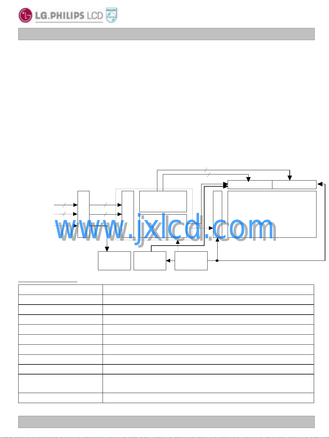
1. General Description
The LP154W02 is a Color Active Matrix Liquid Crystal Display with an integral Cold Cathode Fluorescent
Lamp(CCFL) backlight system. The matrix employs a-Si Thin Film Transistor as the active element.
It is a transmissive type display operating in the normally white mode. This TFT-LCD has 15.4 inches
diagonally measured active display area with WSXGA+ resolution(1680 vertical by 1050 horizontal pixel array)
Each pixel is divided into Red, Green and Blue sub-pixels or dots which are arranged in vertical stripes.
Gray scale or the brightness of the sub-pixel color is determined with a 6-bit gray scale signal for each dot,
thus, presenting a palette of more than 262,144 colors.
The LP154W02 has been designed to apply the interface method that enables low power, high speed,
low EMI. Flat Link must be used as a LVDS(Low Voltage Differential Signaling) chip.
The LP154W02 is intended to support applications where thin thickness, low power are critical factors
and graphic display are important. In combination with the vertical arrangement of the sub-pixels, the
LP154W02 characteristics provide an excellent flat display for office automation products such as
Notebook PC.
LVDS signal(Even)
LVDS signal(Odd)
E-EDID signal
www.jxlcd.com
www.jxlcd.com
General Features
Active screen size
Outline Dimension
Pixel Pitch
Pixel format
Color depth
Luminance, white
Power Consumption
Weight
Display operating mode
Surface treatments
RoHS Comply panel Yes
Mini-Lvds signal(R) Mini-Lvds signal(L)
Mini-lvds
Output
Block
CN1
FlatLink Interface
E-EDID
Block
15.4 inches diagonal
344.0(H)[typ.] x 222.0(V)[typ.] x 6.5(D) mm[Max.]
0.19725 mm x 0.19725mm
1680 horiz. By 1050 vert. Pixels RGB stripes arrangement
6-bit, 262,144 colors
200nit(Center 1point)
5.92W (Typ.) @ LCM circuit 1.75 Watt(Typ.), B/L input 4.17 Watt(Typ.)
550g (Typ), 565(Max)
Transmissive mode, normally white
Hard coating 2H,Anti-glare,Anti-reflection,Anti-electrostatic treatment
of the front polarizer (Nitto Denko AG ARC 150T)
Gamma
Block
Timing
Control
Block
Power
Block
Col. Driver #1~4
Row Driver
Col. Driver #5~8
TFT-LCD
(1680 x 1050)
Ver. 0.1 April. 27, 2007
4 / 32
Liquid Crystal Display
Product Specification
2. Absolute Maximum Ratings
The following are maximum values which, if exceeded, may cause operation or damage to the unit.
Table 1. ABSOLUTE MAXIMUM RATINGS
LP154W02
Parameter symbol
Power Input Voltage
Operating Temperature
Storage Temperature
Operating Ambient Humidity
Storage Humidity
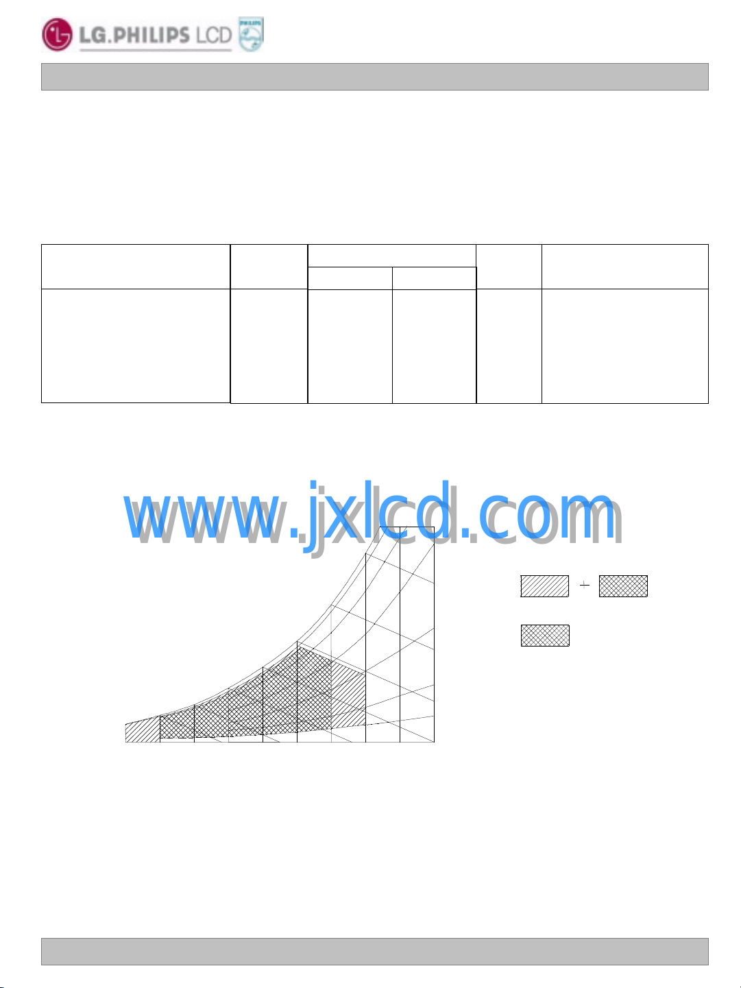
Note : 1. Temperature and relative humidity range are shown in the figure below.
Wet bulb temperature should be 39 °C Max, and no condensation of water.
www.jxlcd.com
www.jxlcd.com
Wet Bulb
Temperature [℃]
10
0
20
V
CC
T
OP
T
ST
H
OP
H
ST
50
40
30
Values
Min. Max.
-0.3
0
-20
10
10
90% 80%
60
4.0
50
60
90
90
Units Notes
Vdc
°C
°C
%RH
%RH
60%
Humidity[(%)RH]
Storage
40%
Operation
20%
10%
At 25 5°C
1
1
1
1
-20
Ver. 0.1 April. 27, 2007
10
20 30 40 50
Dry Bulb Temperature [℃]
60 70 800
5 / 32
LP154W02
Liquid Crystal Display
Product Specification
3. Electrical Specifications
3-1. Electrical Characteristics
The LP154W02 requires two power inputs. One is employed to power the LCD electronics and to
drive the TFT array and liquid crystal. The second input which powers the CCFL, is typically generated
by an inverter. The inverter is an external unit to the LCD.
Table 2. ELECTRICAL CHARACTERISTICS
Parameter Symbol
MODULE
Power Supply Input Voltage
Power Supply Input Current
Differential Impedance
Power Consumption
LAMP
Operating Voltage
Operating Current
Established Starting Voltage
at 25 °C
at 0 °C
Operating Frequency
Discharge Stabilization Time
Power Consumption
Life Time
Note : The design of the inverter must have specification for the lamp in LCD Assembly.
The performance of the Lamp in LCM, for example life time or brightness, is extremely influenced by the
characteristics of the DC-AC inverter. So all the parameters of an inverter should be carefully designed
so as not to produce too much leakage current from high-voltage output of the inverter.
When you design or order the inverter, please make sure unwanted lighting caused by the mismatch of
the lamp and the inverter(no lighting, flicker, etc) never occurs. When you confirm it, the LCD Assembly
should be operated in the same condition as installed in you instrument.
1. The specified typical current and power consumption are under the VCC=3.3V, 25°C,fV=60Hz condition
whereas window XP Bliss pattern is displayed and fV is the frame frequency.
2. This impedance value is needed to proper display and measured from LVDS TX to the mating connector.
3. The variance of the voltage is 10%.
4. The voltage above VS should be applied to the lamps for more than 1 second for start-up.
Otherwise, the lamps may not be turned on.
www.jxlcd.com
www.jxlcd.com
V
I
CC
Zm
P
V
I
V
f
T
P
CC
C
BL
BL
S
BL
S
BL
Min. Max.
3.0
-
90
680
3.0
-
-
40
-
12,000
Values
Typ.
3.3
530
100
1.75
695
6.0
-
-
60
4.17
-
3.6
610
110
2.01
835
6.5
1170
1400
80
3
4.42
-
Units
Vdc
mA
ohm
Watts
V
RMS
mA
V
RMS
V
RMS
kHz
Minutes
Watts
Hrs
Notes
1
2
1
3
4
5
6
7
8
Ver. 0.1 April. 27, 2007
6 / 32
LP154W02
Liquid Crystal Display
Product Specification
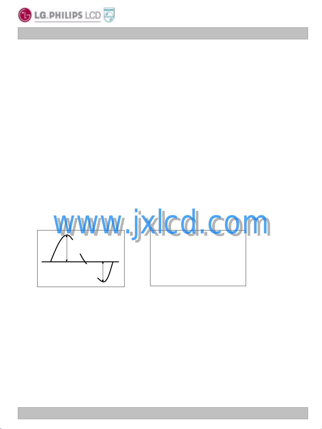
5. The output of the inverter must have symmetrical(negative and positive) voltage waveform and
symmetrical current waveform.(Asymmetrical ratio is less than 10%) Please do not use the inverter
which has asymmetrical voltage and asymmetrical current and spike wave.
Lamp frequency may produce interface with horizontal synchronous frequency and as a result this may
cause beat on the display. Therefore lamp frequency shall be as away possible from the
horizontal synchronous frequency and from its harmonics in order to prevent interference.
6. It is defined the brightness of the lamp after being lighted for 5 minutes as 100%.
TS is the time required for the brightness of the center of the lamp to be not less than 95%.
7. The lamp power consumption shown above does not include loss of external inverter.
The used lamp current is the lamp typical current.
8. The life is determined as the time at which brightness of the lamp is 50% compared to that of initial
value at the typical lamp current on condition of continuous operating at 25 2°C.
9. Do not attach a conducting tape to lamp connecting wire.
If the lamp wire attach to a conducting tape, TFT-LCD Module has a low luminance and the inverter
has abnormal action. Because leakage current is occurred between lamp wire and conducting tape.
10. Requirements for a system inverter design, which is intended to have a better display performance, a
better power efficiency and a more reliable lamp, are following.
It shall help increase the lamp lifetime and reduce leakage current.
a. The asymmetry rate of the inverter waveform should be less than 10%.
b. The distortion rate of the waveform should be within √2 ±10%.
* Inverter output waveform had better be more similar to ideal sine wave.
www.jxlcd.com
www.jxlcd.com
I p
I -p
* Asymmetry rate:
| I p – I –p | / I
* Distortion rate
I p (or I –p) / I
rms
rms
* 100%
Ver. 0.1 April. 27, 2007
7 / 32
LP154W02
Liquid Crystal Display
Product Specification
3-2. Interface Connections
Interface chip must be used FlatLink, part No. THC63LVDF823A(Transmitter made by Thine Inc or
equivalence.)
This LCD employs two interface connections, a 30-pin-connector is used for the module electronics and the
other connector is used for the integral backlight system.
The electronics interface connector is a model FI-XB30SR-HF11 manufactured by JAE.
The pin configuration for the connector is shown in the table below.
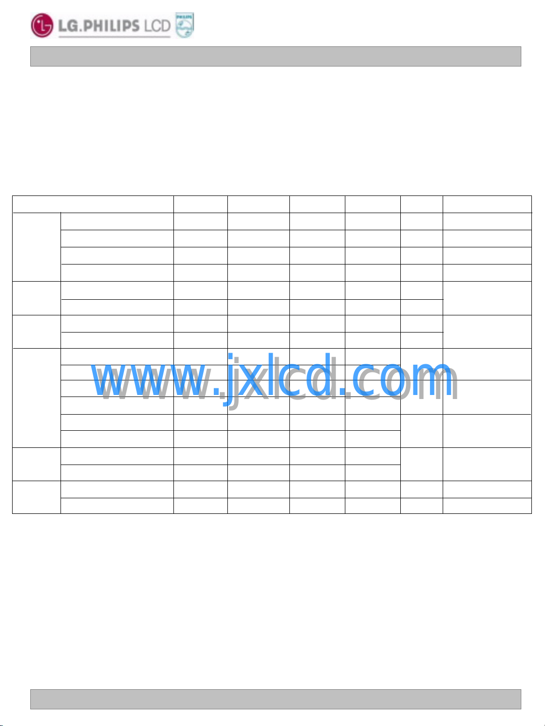
Table 3. MODULE CONNECTOR PIN CONFIGURATION(LVDS)
Pin Symbol Description Notes
1
2
3
4
5
6
7
8
9
10
11
12
13
14
15
16
17
18
19
20
21
22
23
24
25
26
27
28
29
30
GND
Vcc
Vcc
VEDID
NC
CLKEDID
DATAEDID
Odd_A1M
Odd_A1P
GND
Odd_A2M
Odd_A2P
GND
Odd_A3M
Odd_A3P
www.jxlcd.com
GND
www.jxlcd.com
Odd_CLKM
Odd_CLKP
GND
Even_A1M
Even_A1P
GND
Even_A2M
Even_A2P
GND
Even_A3M
Even_A3P
GND
Even_CLKM
Even_CLKP
Ground
Power(3.3V)
Power(3.3V)
DDC 3.3V Power
No connect
DDC clock
DDC data
Differential Signal
Differential Signal
Ground
Differential Signal
Differential Signal
Ground
Differential Signal
Differential Signal
Ground
Differential Signal
Differential Signal
Ground
Differential Signal
Differential Signal
Ground
Differential Signal
Differential Signal
Ground
Differential Signal
Differential Signal
Ground
Differential Signal
Differential Signal
1. Interface chips
1.1 LCD : DTML012(LCD Controller)
including LVDS Receiver
1.2 System : THC63LVD823 or equivalent
*Pin to Pin compatible with TI LVDS
2. Connector
2.1 LCD : FI-XB30SR-HF11,JAE or equivalent
2.2 Mating : FI-X30M or equivalent.
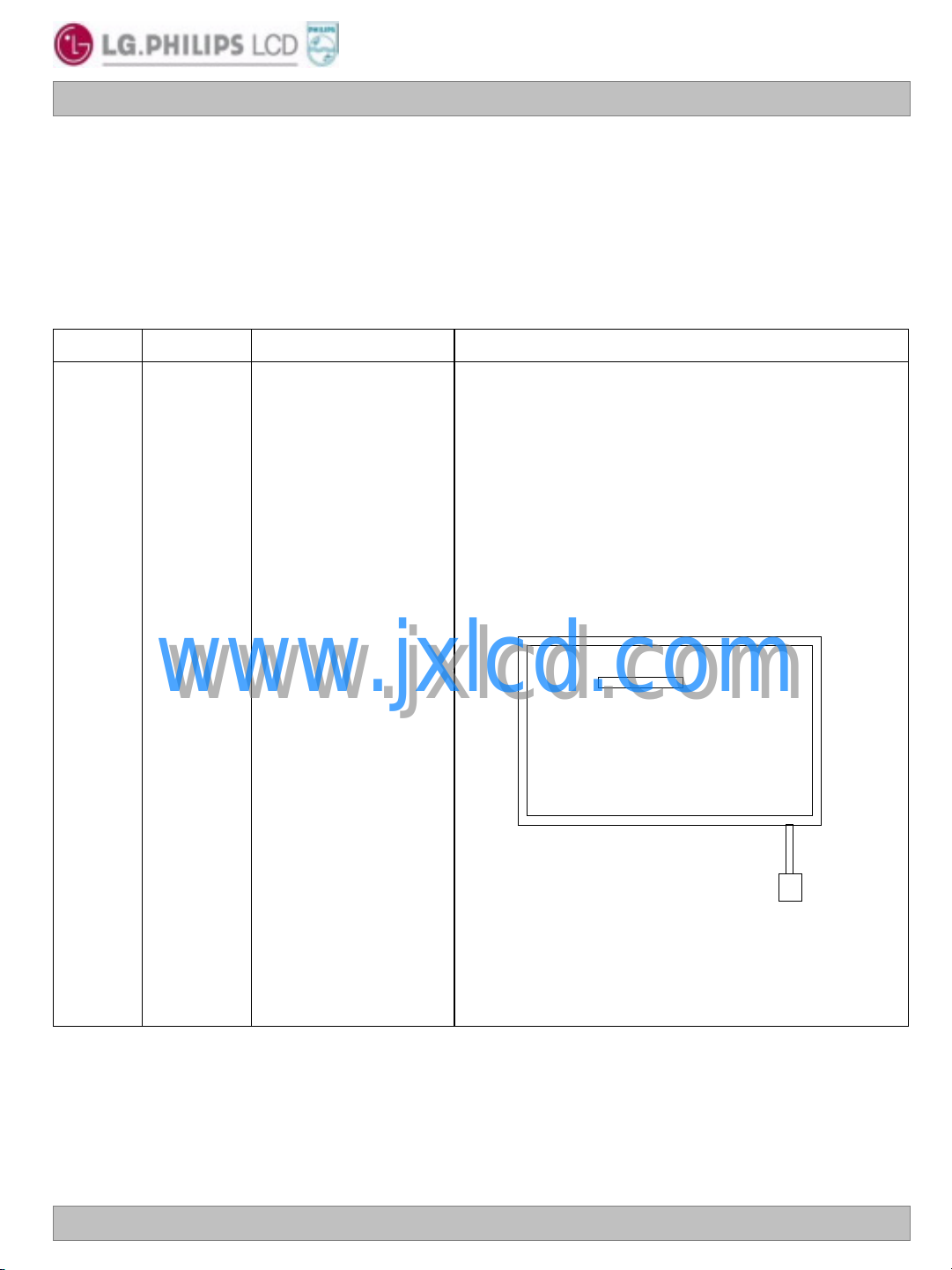
2.3 Connector pin arrangement
1
Viewing on Display side
30
CN1
CN2
Ver. 0.1 April. 27, 2007
8 / 32
LP154W02
Liquid Crystal Display
Product Specification
The backlight interface connector is a model BHSR-02VS-1, manufactured by JST or equivalent.
The mating connector part number is SM02B-BHSS-1 or equivalent.
The pin configuration for the connector is shown in the table below.
Table 4. BACKLIGHT CONNECTOR PIN CONFIGURATION
Pin Symbol Description Notes
1
2
Notes : 1. The high voltage side terminal is colored White. The low voltage side terminal is Yellow.
HV
LV
www.jxlcd.com
www.jxlcd.com
Power supply for lamp
(High voltage side)
Power supply for lamp
(Low voltage side)
1
1
Ver. 0.1 April. 27, 2007
9 / 32
LP154W02
Liquid Crystal Display
Product Specification
3-3. Signal Timing Specifications
This is the signal timing required at the input of the LVDS Transmitter. All of the interface signal timing
should be satisfied with the following specifications for its proper operation.
Table 6. Timing Table
Dclk
Hsync
Vsync
DE
DATA
Input
Voltage
ITEM
Frequency
Width-Low
Width-High
Period
Period t
Width active
Set up Time
Hold Time
Horizontal Back Porch
www.jxlcd.com
www.jxlcd.com
Horizontal Front Porch
Vertical Back Porch
Vertical Front Porch
Set up Time
Hold Time
High
Low
SYMBOL
f
CLK
t
WCL
t
WCH
D
t
HP 864 1288
t
WH
VP
t
WV 1 -
t
SI
t
HI
t
HBP
t
HFP 8 -
t
VBP
t
VFP
t
SD
t
HD
t
rH
t
rL
MIN TYP. MAX. UNIT NOTES
61
3 - - ns
3 - - ns
0.4 0.6Duty
-
-
0.5
952
8 -Width
1057
32
1066
3
-
3
3
-
-
8 64 -
16
5 12 -
1
3
3
1
-
-
-
-
0.7Vcc
1082
-
-
-
-
-
0.3Vcc
MHz6755
t
t
t
ns
t
ns
CLK
CLK
HP
t
CLK
t
HP
HP
D= t
CLKH /tCLK
For Dclk
For Dclk
Ver. 0.1 April. 27, 2007
10 / 32
 Loading...