

Product Specification
SPECIFICATION
LP150X09
Liquid Crystal Display
FOR
APPROVAL
)
(
(
Preliminary Specification
)
Final Specification
◆
MODEL
www.jxlcd.com
www.jxlcd.com
15.0” XGA TFT LCDTitle
GeneralBUYER
*When you obtain standard approval,
please use the above model name without suffix
LG.Philips LCD Co., Ltd.SUPPLIER
LP150X09*MODEL
B5K8Suffix
SIGNATUREAPPROVED BY
/
/
/
Please return 1 copy for your confirmation with
your signature and comments.
Ver. 1.1 Oct. 23. 2007
SIGNATUREAPPROVED BY
S. C. Yoon / S.Manager
REVIEWED BY
G.J. Han / Manager
J.W. Park / Manager
PREPARED BY
I. Y. Jung / Engineer
J.H. Kim / Engineer
Products Engineering Dept.
LG. Philips LCD Co., Ltd
1 / 27
Product Specification
Contents
LP150X09
Liquid Crystal Display
ITEMNo
COVER
CONTENTS
RECORD OF REVISIONS
GENERAL DESCRIPTION1
ABSOLUTE MAXIMUM RATINGS2
ELECTRICAL SPECIFICATIONS3
ELECTRICAL CHARACTERISTICS 3-1
INTERFACE CONNECTIONS 3-2
SIGNAL TIMING SPECIFICATIONS 3-3
SIGNAL TIMING WAVEFORMS 3-4
COLOR INPUT DATA REFERNECE 3-5
www.jxlcd.com
www.jxlcd.com
POWER SEQUENCE 3-6
OPTICAL SFECIFICATIONS4
MECHANICAL CHARACTERISTICS5
Page
1
2
3
4
5
6
7
9
9
10
11
12
16
RELIABILITY6
INTERNATIONAL STANDARDS7
SAFETY 7-1
EMC 7-2
PACKING8
DESIGNATION OF LOT MARK 8-1
PACKING FORM 8-2
PRECAUTIONS9
APPENDIX. Enhanced Extended Display Identification Data A
Ver. 1.1 Oct. 23. 2007
20
21
21
22
22
23
25
2 / 27
Product Specification
RECORD OF REVISIONS
LP150X09
Liquid Crystal Display
DescriptionPageRevision DateRevision No
-12. 10. 20051.0
Final Specifications
4
Power consumption changed
Electrical characteristics changed6
10. 23. 20071.1
www.jxlcd.com
www.jxlcd.com
LCD Interface chip changed7
Timing table updated9
color coordinates changed12
EDID
Ver.
1.0
1.0
Ver. 1.1 Oct. 23. 2007
3 / 27
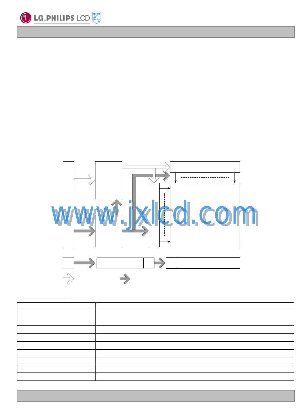
LP150X09
CN1
LVDS
&
Timing
Control
Block
Power
Block
Column Driver Circuit
Row Dirver Circuit
TFT-LCD
(1024 X 768)
J1
:Control & Data :Power
B/L Inverter
J2
Backlight Ass'y
J3
Liquid Crystal Display
Product Specification
1. General Description
The LP150X09 is a Color Active Matrix Liquid Crystal Display with an integral Cold Cathode Fluorescent
Lamp (CCFL) backlight system. The matrix employs a-Si Thin Film Transistor as the active element. It is a
transmissive type display operating in the normally white mode. This TFT-LCD has 15.0 inches diagonally
measured active display area with XGA resolution(768 vertical by 1024 horizontal pixel array). Each pixel is
divided into Red, Green and Blue sub-pixels or dots which are arranged in vertical stripes. Gray scale or the
brightness of the sub-pixel color is determined with a 6-bit gray scale signal for each dot, thus, presenting a
palette of more than 262,144 colors.
The LP150X09 has been designed to apply the interface method that enables low power, high speed, low
EMI.
The LP150X09 is intended to support applications where thin thickness, low power are critical factors and
graphic displays are important. In combination with the vertical arrangement of the sub-pixels, the LP150X09
characteristics provide an excellent flat display for office automation products such as Notebook PC.
General Features
www.jxlcd.com
www.jxlcd.com
15.0 inches(38.1cm) diagonal Active Screen Size
317.3(H) × 241.5(V) × 5.7(D) mm (Typ.)Outline Dimension
0.297 mm × 0.297 mm Pixel Pitch
1024 horiz. By 768 vert. Pixels RGB strip arrangementPixel Format
6-bit, 262,144 colorsColor Depth
180 cd/m2(Typ.), 5p averageLuminance, White
Total 4.96 Watt (Typ.)Power Consumption
575 g(Max.) with inverter and bracketWeight
Transmissive mode, normally whiteDisplay Operating Mode
Hard coating(3H) Anti-glare treatment of the front polarizerSurface Treatment
Ver. 1.1 Oct. 23. 2007
4 / 27
LP150X09
Liquid Crystal Display
Product Specification
2. Absolute Maximum Ratings
The following are maximum values which, if exceeded, may cause faulty operation or damage to the unit.
Table 1. ABSOLUTE MAXIMUM RATINGS
Parameter Notes
Power Input Voltage
Operating Temperature
Storage Temperature
Operating Ambient Humidity
Storage Humidity
Note : 1. Temperature and relative humidity range are shown in the figure below.
Wet bulb temperature should be 39C Max, and no condensation of water.
www.jxlcd.com
www.jxlcd.com
Wet Bulb
Temperature [℃]
20
10
0
Symbol
60
50
40
30
Values
MaxMin
90% 80%
60%
40%
20%
10%
Units
Humidity[(%)RH]
Storage
Operation
at 25 5CVdc4.0-0.3VCC
1C500TOP
1C60-20HST
1%RH9010HOP
1%RH9010HST
-20
Ver. 1.1 Oct. 23. 2007
10
20 30 40 50
Dry Bulb Temperature [℃]
60 70 800
5 / 27
LP150X09
Liquid Crystal Display
Product Specification
3. Electrical Specifications
3-1. Electrical Characteristics
The LP150X09 requires two power inputs. One is employed to power the LCD electronics and to drive the
TFT array and liquid crystal. The second input which powers the CCFL, is typically generated by an
inverter. The inverter is an external unit to the LCD.
Table 2. ELECTRICAL CHARACTERISTICS
Parameter Symbol
MODULE :
Power Supply Input Current
Differential Impedance
LAMP :
Operating Voltage
Operating Current
Operating Frequency
INVERTER :
Input Voltage
Input Current
Input Power Consumption
Output Voltage
Output Power Consumption
Open Lamp Voltage
Striking Time
www.jxlcd.com
www.jxlcd.com
OUT
OUT
CC
Zm
BL
BL
BL
IN
IN
IN
OUT
_FF Output Current (Aging 30minutes)
_00
OUT
OPEN
S
Values
DC
RMS
RMS
DC
DC
DC
RMS
RMS
RMS
RMS
NotesUnit
1mA260230-I
1Watt0.860.76-Pc Power Consumption
2Ohm11010090
3mA
4Min3--Ts Discharge Stabilization Time
5Hrs--15,000 Life Time
6mA-360-I
6W-5.18-P
7V
7mA
7KHz65-45Freq. Operating Frequency
6W4.914.283.65P
8V
9%--75 Efficiency
8sec1.4-0.6T
MaxTypMin
3.63.33.0VCC Power Supply Input Voltage
870(2.0mA)665(6.3mA)630(7.0mA)V
7.06.32.0I
21.014.47.5V
5.25-2.0FPVEE_High Backlight On/Off Control
0.8--0.3FPVEE_Low
780680580V
--2I
6.66.36.0I
1800-1400V
V
V
kHz806550f
V
V
V
Hex00-FF Backlight Adjust (IBL Control)
mA
Note)
1. The specified current and power consumption are under the Vcc = 3.3V , 25℃, fv = 60Hz condition
whereas Mosaic Pattern is displayed and fv is the frame frequency.
2. This impedance value is needed to proper display and measured form LVDS Tx to the mating connector.
3. The typical operating current is for the typical surface luminance (LWH) in optical characteristics.
Ver. 1.1 Oct. 23. 2007
6 / 27
LP150X09
Liquid Crystal Display
Product Specification
Note)
4. Define the brightness of the lamp after being lighted for 5 minutes as 100%, Ts is the time required for
the brightness of the center of the lamp to be not less than 95%.
5. The life time is determined as the time at which brightness of lamp is 50% compare to that of initial value
at the typical lamp current.
6. VIN = 14.4V(Typ.), 28_H
7. SMData=00_H
8. No Load, SMData=00_H.
9. VIN =7.5V(Min.), 00H.
3-2. Interface Connections
This LCD employs two interface connections, a 30 pin connector is used for the module electronics interface
and the other connector is used for the integral backlight system.
The electronics interface connector is a model FI-XB30SRL-HF11 manufactured by JAE.
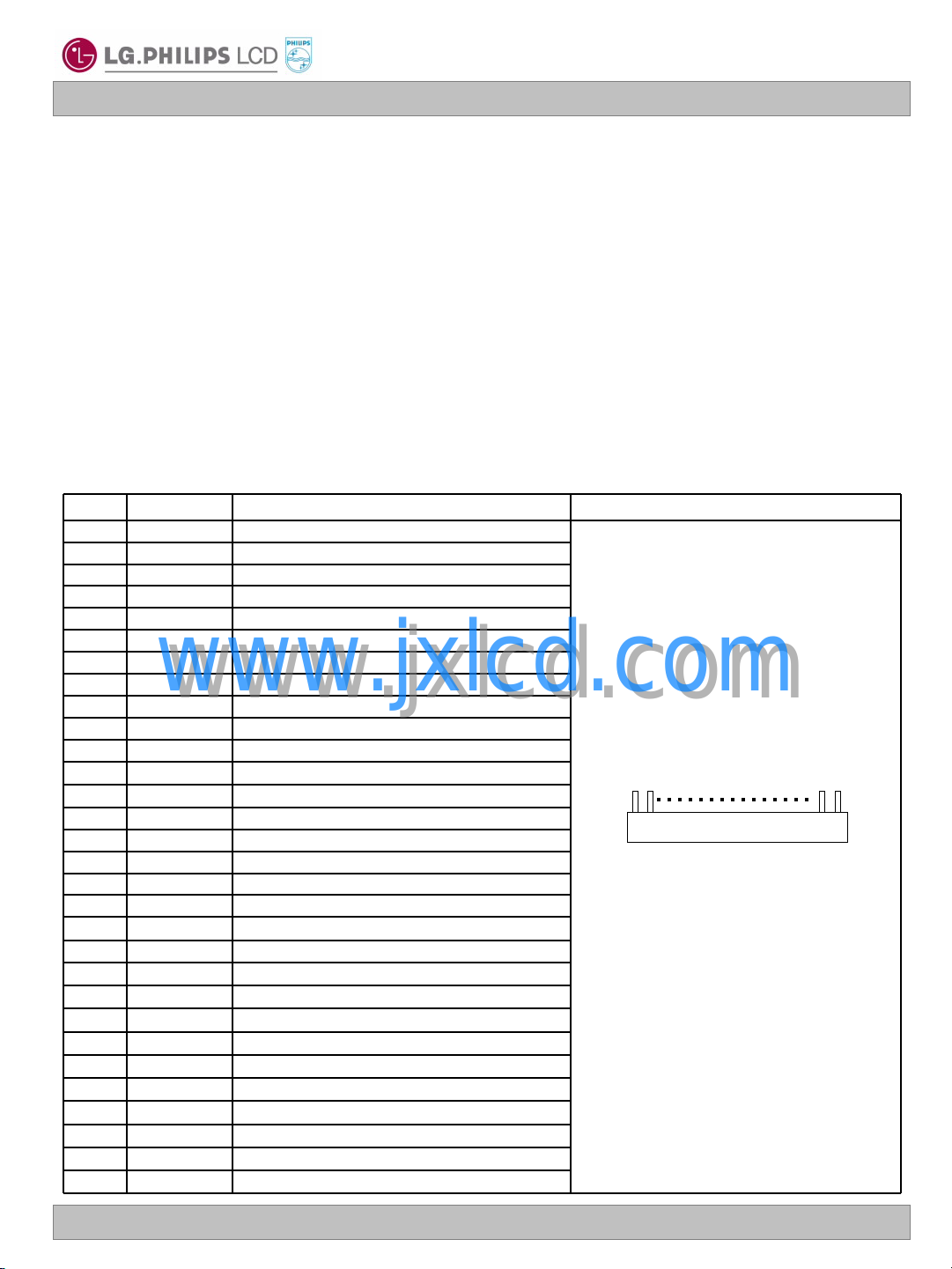
Table 3. MODULE CONNECTOR PIN CONFIGURATION (CN1)
NotesDescriptionSymbolPin
GroundGND1
Power Supply, 3.3V Typ.VCC2
Power Supply, 3.3V Typ.VCC3
1, Interface chips
1.1 LCD : SiW, SiWLVDSRx
1.2 System : it must include international
standard LVDS Transmitter.
* Pin to Pin compatible with LVDS
2. Connector
2.1 LCD : FI-XB30SRL-HF11, JAE or
MDF76LBRW-30S-1H, HIROSE
2.2 Mating : FI-X30M or equivalent.
2.3 Connector pin arrangement
30
[LCD Module Rear View]
1
10
11
12
13
14
15
16
17
18
19
20
21
22
23
24
25
26
27
28
29
30
4
5
6
7
8
9
www.jxlcd.com
www.jxlcd.com
RIN 1- Negative LVDS differential data input
NC
GND
DDC 3.3V powerV EEDID
Reserved for supplier Bist test pointBIST
DDC ClockClk EEDID
DDC DataDATA EEDID
Negative LVDS differential data inputRIN 0-
Positive LVDS differential data inputRIN 0+
GroundGND
Positive LVDS differential data inputRIN 1+
GroundGND
Negative LVDS differential data inputRIN 2-
Positive LVDS differential data inputRIN 2+
GroundGND
Negative LVDS differential clock inputCLKIN-
Positive LVDS differential clock inputCLKIN+
GroundGND
No connectionNC
No connection
Ground
No connectionNC
No connectionNC
GroundGND
No connectionNC
No connectionNC
GroundGND
No connectionNC
No connectionNC
Ver. 1.1 Oct. 23. 2007
7 / 27
LP150X09
Liquid Crystal Display
Product Specification
The inverter interface connector(J1) is a LVC-D20SFYG model manufactured by Honda. The pin configuration
for the connector is shown in the table below.
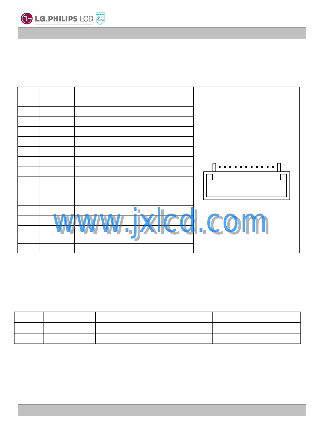
Table 4. BACKLIGHT INVERTER CONNECTOR PIN CONFIGURATION (J1)
NotesDescriptionSymbolPin
2
3
14
V
IN
IN
IN
www.jxlcd.com
www.jxlcd.com
LAMP_STAT
Power for the inverter 1
Power for the inverter V
Power for the inverter V
No connectionNC4
GroundGND5
Power for the control circuit5V_SUS6
Power for storing a brightness values5V_ALW7
GroundGND8
Brightness dataSMB_DAT9
Clock for brightness dataSMB_CLK10
GroundGND11
Enable for lamp turn on and offFPVEE12
GroundGND13
Lamp status (Feedback, Lamp On = 5V,
Lamp Off 0V), from control chip
No ConnectionNC15~20
[Connector]
LVC-D20SFYG, Honda
[Connector pin arrangement]
1 20
The backlight interface connector is a model BHSR-02VS-1, manufactured by JST or a model 1376176-1,
manufactured by AMP. The mating connector part number is SM02B-BHSS-1 or equivalent.
Table 5. BACKLIGHT CONNECTOR PIN CONFIGURATION (J3)
NotesDescriptionSymbolPin
1Power supply for lamp (High voltage side)HV1
1Power supply for lamp (Low voltage side)LV2
Notes : 1. The high voltage side terminal is colored pink and the low voltage side terminal is white
Ver. 1.1 Oct. 23. 2007
8 / 27
LP150X09
Liquid Crystal Display
Product Specification
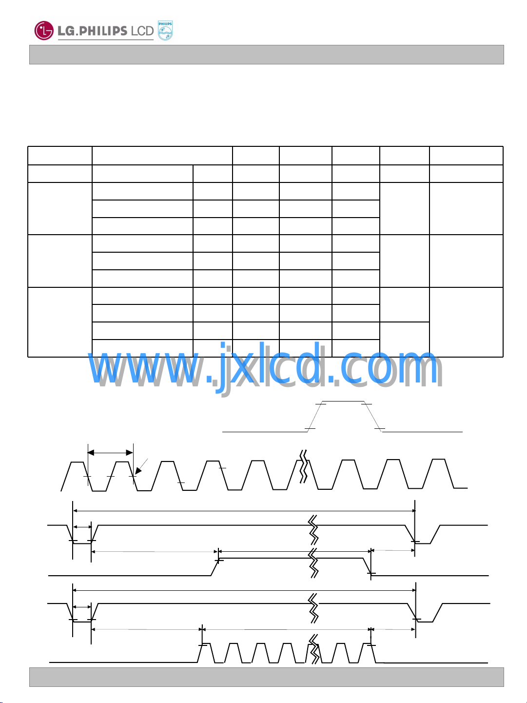
3-3. Signal Timing Specifications
This is the signal timing required at the input of the User connector. All of the interface signal timing should be
satisfied with the following specifications and specifications of LVDS Tx/Rx for it’s proper operation.
Table 6. TIMING TABLE
NoteUnitMaxTypMinSymbolITEM
Vsync
Data
Enable
3-4. Signal Timing Waveforms
www.jxlcd.com
www.jxlcd.com
Data Enable, Hsync, Vsync
DCLK
tCLK
0.5 Vcc
fCLK FrequencyDCLK
tHPPeriodHsync
tWH Width
tWHA Width-Active
tVP Period
tWV Width
tWVA Width-Active
tHBPHorizontal back porch
tHFPHorizontal front porch
tVBPVertical back porch
tVFPVertical front porch
High: 0.7VCC
Low: 0.3VCC
136413441206
3081368
102410241024
830806780
5461
768768768
31616010
3162410
60297
5431
tCLK
tHP
tCLK
tHP
Condition : VCC =3.3V
15.4nsMHz686562
t
HP
Hsync
Data Enable
Vsync
Ver. 1.1 Oct. 23. 2007
t
WH
t
WV
Data Enable
t
VBP
t
HBP
tWHA
t
VP
tWVA
t
t
HFP
VFP
9 / 27
 Loading...