


LP150X08
Liquid Crystal Display
Product Specification
SPECIFICATION
FOR
APPROVAL
)
(
(
Preliminary Specification
)
Final Specification
◆
15.0” XGA TFT LCDTitle
PROJECT
www.jxlcd.com
www.jxlcd.com
GeneralBUYER
DATESIGNATURE
/
/
/
APPROVED BY
J. H. Lee / S.Manager
REVIEWED BY
G. J. Han / Manager
PREPARED BY
I. Y. Jung / Engineer
LG.Philips LCD Co., Ltd.SUPPLIER
LP150X08*MODEL
A5N2Suffix
SIGNATURE
/ DATE
Please return 1 copy for your confirmation with
your signature and comments.
Ver. 0.1 Oct. 1. 2004
Products Engineering Dept.
LG. Philips LCD Co., Ltd
1 / 27
COVER
CONTENTS
RECORD OF REVISIONS
GENERAL DESCRIPTION1
ABSOLUTE MAXIMUM RATINGS2
LP150X08
Liquid Crystal Display
Product Specification
Contents
PageITEMNo
1
2
3
4
5
ELECTRICAL SPECIFICATIONS3
ELECTRICAL CHARACTREISTICS 3-1
INTERFACE CONNECTIONS 3-2
SIGNAL TIMING SPECIFICATIONS 3-3
SIGNAL TIMING WAVEFORMS 3-4
COLOR INPUT DATA REFERNECE 3-5
POWER SEQUENCE 3-6
OPTICAL SFECIFICATIONS4
www.jxlcd.com
MECHANICAL CHARACTERISTICS5
www.jxlcd.com
RELIABLITY6
INTERNATIONAL STANDARDS7
SAFETY 7-1
EMC 7-2
PACKING8
DESIGNATION OF LOT MARK 8-1
PACKING FORM 8-2
PRECAUTIONS9
9-1
9-4
MOUNTING PRECAUTIONS
OPERATING PRECAUTIONS 9-2
ELECTROSTATIC DISCHARGE CONTROL 9-3
PRECAUTIONS FOR STRONG LIGHT EXPOSURE
STORAGE 9-5
HANDLING PRECAUTIONS FOR PROTECTION FILM 9-6
APPENDIX. Enhanced Extended Display Identification DataA
6
6
8
9
9
10
11
12
16
20
21
21
21
22
22
22
23
23
23
24
24
24
24
25
Ver. 0.1 Oct. 1. 2004
2 / 27
Product Specification
RECORD OF REVISIONS
LP150X08
Liquid Crystal Display
0.0
0.1 Oct. 1.2004
Sep.15.2004
www.jxlcd.com
www.jxlcd.com
DescriptionPageRevision DateRevision No
-
First Draft (Preliminary)
Changed item : Lamp operating current and voltage
6
Added item : Note 4.
EDID
Ver.
0.0
0.0
Ver. 0.1 Oct. 1. 2004
3 / 27
LP150X08
Liquid Crystal Display
Product Specification
1. General Description
The LP150X08 is a Color Active Matrix Liquid Crystal Display with an integral Cold Cathode Fluorescent
Lamp(CCFL) backlight system. The matrix employs a-Si Thin Film Transistor as the active element.
It is a transmissive type display operating in the normally white mode. This TFT-LCD has 15.0 inches
diagonally measured active display area with XGA resolution(768 vertical by 1024 horizontal pixel array)
Each pixel is divided into Red, Green and Blue sub-pixels or dots which are arranged in vertical stripes.
Gray scale or the brightness of the sub-pixel color is determined with a 6-bit gray scale signal for each dot,
thus, presenting a palette of more than 262,144 colors.
The LP150X08 has been designed to apply the interface method that enables low power, high speed,
low EMI.
The LP150X08 is intended to support applications where thin thickness, low power are critical factors
and graphic display are important. In combination with the vertical arrangement of the sub-pixels, the
LP150X08 characteristics provide an excellent flat display for office automation products such as
Notebook PC.
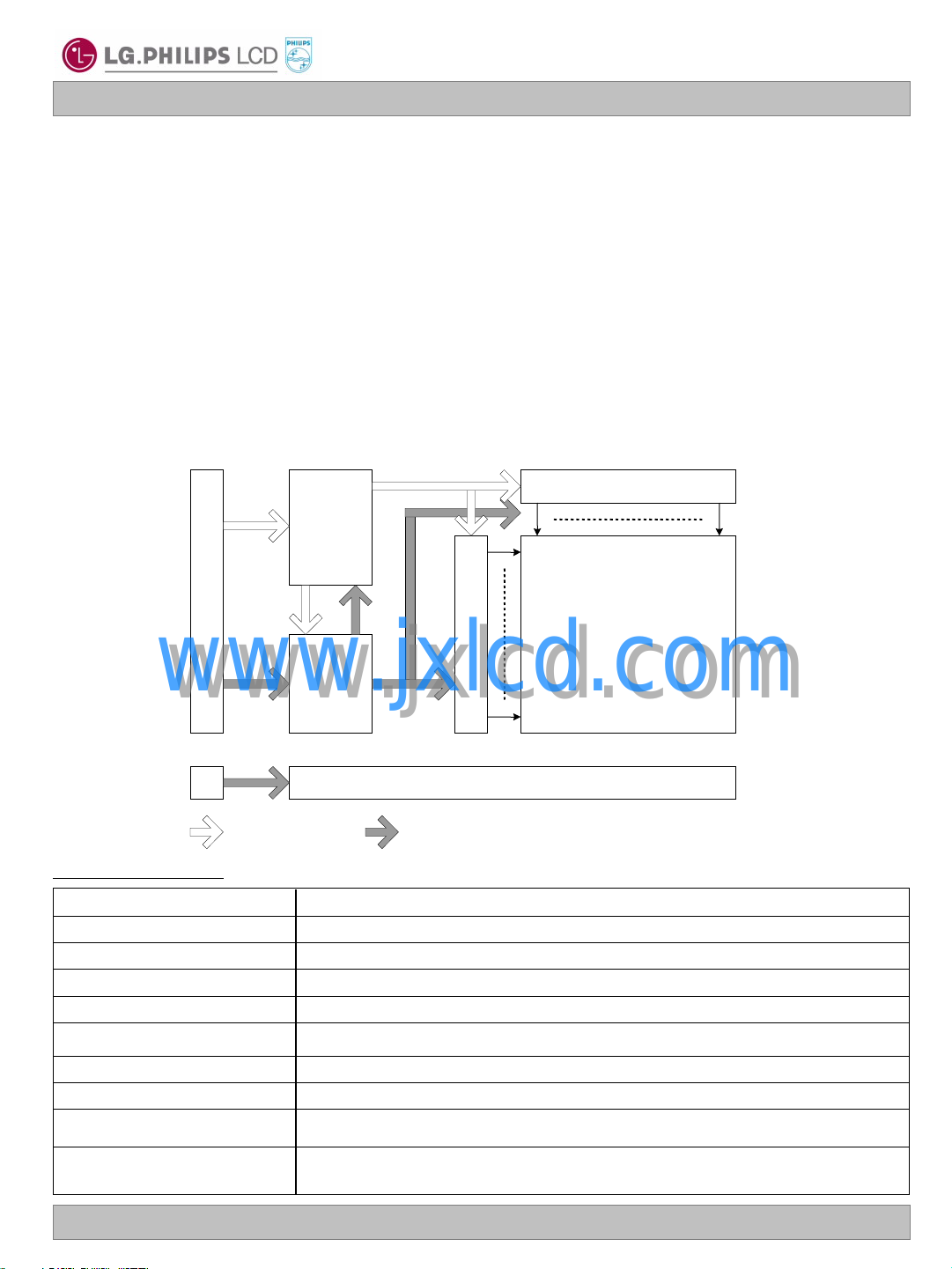
CN 1
www.jxlcd.com
www.jxlcd.com
General Features
Color Depth
LVDS
&
Timing
Control
Block
Power
Block
:Control & Data :Power
15.0 inches(38.1cm) diagonalActive Screen Size
317.3(H) x 241.5(V) x 5.7(D) mm(Typ.)Outline Dimension
0.297 mm x 0.297 mmPixel Pitch
1024 horiz. By 768 vert. Pixels RGB strip arrangementPixel Format
6-bit, 262,144 colors
150 cd/m2(Typ.)Luminance, White (5P)
4.66WPower Consumption
540 g (Typ.) Weight
Column Driver Circuit
TFT-LCD
(1024 X 768)
Row Driver Circuit
Backlight Lamp Ass'yJ1
Transmissive mode, normally whiteDisplay Operating Mode
Surface Treatment
Ver. 0.1 Oct. 1. 2004
Hard coating(3H) Anti-glare treatment of the front polarizer
4 / 27
LP150X08
Liquid Crystal Display
Product Specification
2. Absolute Maximum Ratings
The following are maximum values which, if exceeded, may cause faulty operation or damage to the unit.
Table 1. ABSOLUTE MAXIMUM RATINGS
Parameter Notes
Power Input Voltage-ON
Power Input Voltage-OFF
Operating Temperature
Storage Temperature
Operating Ambient
Humidity
Storage Humidity
Electrostatic Durability
(ESD)
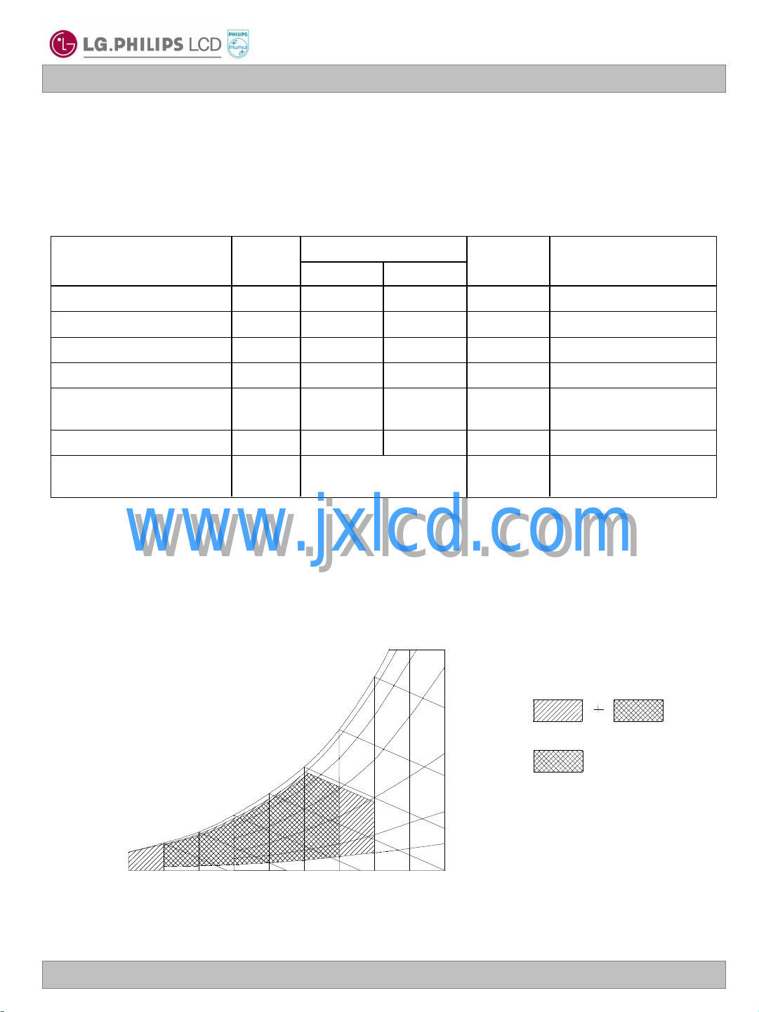
Note : 1. Temperature and relative humidity range are shown in the figure below.
Wet bulb temperature should be 39C Max, and no condensation of water.
2. Condition 1) Non-operation, 150㎊-330Ω, 25℃, 40~60%RH
2) I/F Connector pins are subjected.
3) The surface of Metal bezel and LCD are subjected.
4) Discharge interval time 1sec, 10 times each place
www.jxlcd.com
www.jxlcd.com
Symbol
VESD
Values
MaxMin
90% 80%
Units
kV± 8.0
at 25 5CVdc4.02.7VCC
at 25 5CVdc0.3-0.3GND
1C500TOP
1C60-20TST
1%RH9010HOP
1%RH9010HST
2
60
Wet Bulb
Temperature [℃]
30
20
10
0
-20
Ver. 0.1 Oct. 1. 2004
10
20 30 40 50
Dry Bulb Temperature [℃]
50
40
60 70 800
60%
Humidity[(%)RH]
Storage
40%
Operation
20%
10%
5 / 27
LP150X08
Liquid Crystal Display
Product Specification
3. Electrical Specifications
3-1. Electrical Characteristics
The LP150X08 requires two power inputs. One is employed to power the LCD electronics and to drive the
TFT array and liquid crystal. The second input which powers the CCFL, is typically generated by an
inverter. The inverter is an external unit to the LCD.
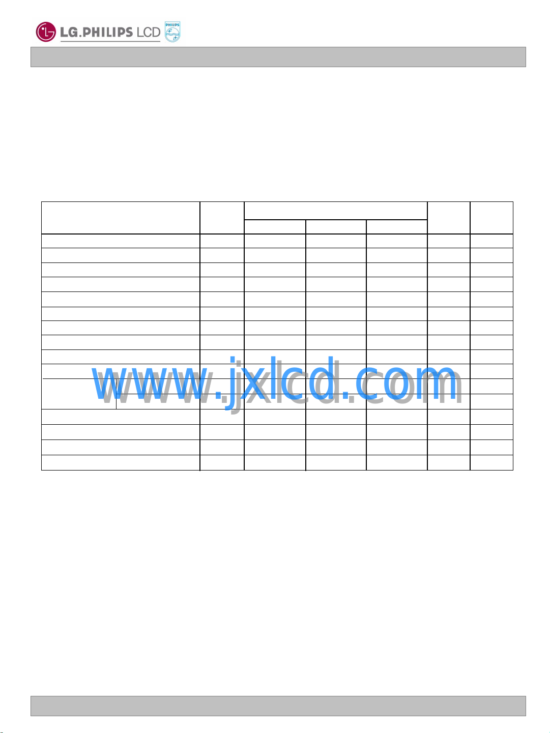
Table 2. ELECTRICAL CHARACTERISTICS
Parameter Symbol
MODULE :
Power Supply Input Current
LAMP :
Operating Voltage
Operating Current
www.jxlcd.com
www.jxlcd.com
Operating Frequency
Discharge Stabilization Time
Power Consumption
Life Time
Note : The design of the inverter must have specifications for the lamp in LCD Assembly.
The performance of the Lamp in LCM, for example life time or brightness, is extremely influenced by
the characteristics of the DC-AC inverter. So all the parameters of an inverter should be carefully
designed so as not to produce too much leakage current from high-voltage output of the inverter.
When you design or order the inverter, please make sure unwanted lighting caused by the mismatch of
the lamp and the inverter(no lighting, flicker, etc) never occurs. When you confirm it, the LCD–
Assembly should be operated in the same condition as installed in you instrument.
1. The specified current and power consumption are under the VCC=3.3V, 25C, fV=60Hz condition
whereas Mosaic pattern is displayed and fV is the frame frequency.
2. This impedance value is needed to proper display and measured from LVDS TX to the mating
connector.
3. The variance of the voltage is 10%.
4. FOS, and reliability test condition is at 6.0mA
5. The voltage above VS should be applied to the lamps for more than 1 second for start-up.
Otherwise, the lamps may not be turned on. The used lamp current is the lamp typical current.
at 25 C
at 0 C
CC
Zm Differential Impedance
BL
BL
BL
BL
Values
MaxTypMin
Vdc3.63.33.0VCC Power Supply Input Voltage
805685640V
6.55.02.0I
1140-1370--
mA
V
V
RMS
RMS
RMS
NotesUnit
1mA265230-I
1Watt0.870.76-Pc Power Consumption
2ohm11010090
3V
RMS
4Vs Established Starting Voltage
5kHz805845f
6Min3--Ts
7Watt4.33.9-P
8Hrs--10,000
Ver. 0.1 Oct. 1. 2004
6 / 27
LP150X08
Liquid Crystal Display
Product Specification
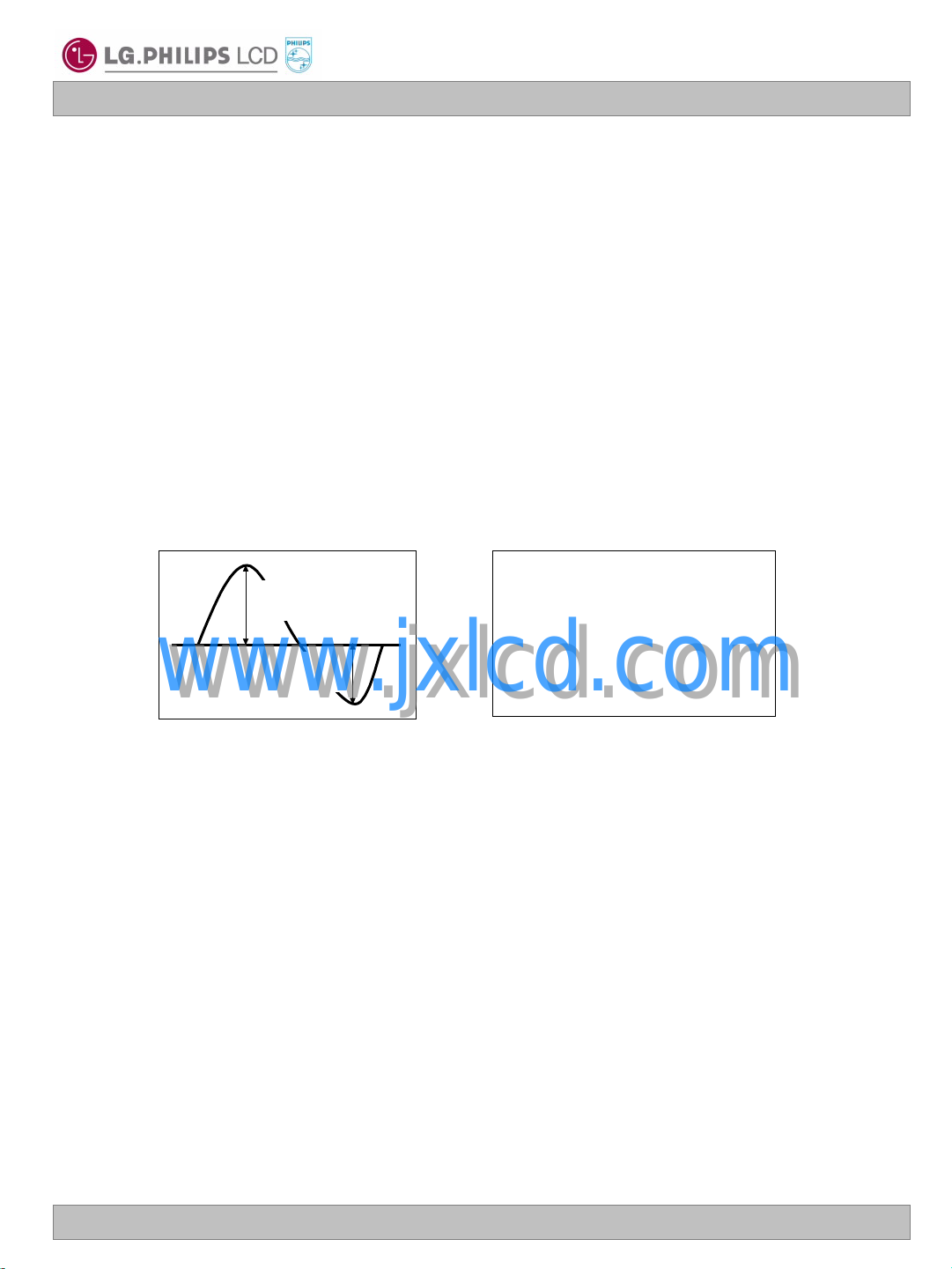
5. The output of the inverter must have symmetrical(negative and positive) voltage waveform and
symmetrical current waveform.(Unsymmetrical ratio is less than 10%) Please do not use the inverter
which has unsymmetrical voltage and unsymmetrical current and spike wave.
Lamp frequency may produce interface with horizontal synchronous frequency and as a result this may
cause beat on the display. Therefore lamp frequency shall be as away possible from the horizontal
synchronous frequency and from its harmonics in order to prevent interference.
6. Let’s define the brightness of the lamp after being lighted for 5 minutes as 100%.
TS is the time required for the brightness of the center of the lamp to be not less than 95%.
7. The lamp power consumption shown above does not include loss of external inverter.
The used lamp current is the maximum lamp current (6.0mA
8. The life is determined as the time at which brightness of the lamp is 50% compared to that of initial
value at the maximum lamp current(6.0mA
9. Requirements for a system inverter design, which is intended to have a better display performance, a
better power efficiency and a more reliable lamp, are following.
It shall help increase the lamp lifetime and reduce leakage current.
a. The asymmetry rate of the inverter waveform should be less than 10%.
b. The distortion rate of the waveform should be within 2 10%.
* Inverter output waveform had better be more similar to ideal sine wave.
) on condition of continuous operating at 25 2C
RMS
RMS
).
* Asymmetry rate:
I p
I -p
www.jxlcd.com
www.jxlcd.com
※ Do not attach a conducting tape to lamp connecting wire.
If the lamp wire attach to a conducting tape, TFT-LCD Module has a low luminance and the inverter
has abnormal action. Because leakage current is occurred between lamp wire and conducting tape.
| I p – I –p | / I
* Distortion rate
I p (or I –p) / I
* 100%
rms
rms
Ver. 0.1 Oct. 1. 2004
7 / 27

LP150X08
Liquid Crystal Display
Product Specification
3-2. Interface Connections
The interface connections are compatible with ISP (Industry Standard Panels) 15.0” Mounting and Top
Level Interface Requirements (Version2, June,2000) defined by SPWG (Standard Panels Working
Group). This LCD employs two interface connections, a 30 pin connector is used for the module electronics
and the other connector is used for the integral backlight system.
The electronics interface connector is a model GT101-30S-HR11 manufactured by LG Cable. The pin
configuration for the connector is shown in the table below.
Table 3. MODULE CONNECTOR PIN CONFIGURATION (CN1)
NotesDescriptionSymbolPin
VSS Ground1
Power Supply, 3.3V Typ.VCC2
Power Supply, 3.3V Typ.VCC3
DDC 3.3V powerVEDID4
No ConnectionNC5
DDC ClockClkEDID6
DATAEDID
7
Note: All GND(ground) pins should be connected together and to GND which should also be
the LCD’s metal frame. All VCC (power input) pins should be connected together.
part number is SM02B-BHSS-1 or equivalent.
DDC Data
- LVDS differential data input (R0-R5, G0)RIN 0 - 8
+ LVDS differential data input (R0-R5, G0)RIN 0 +9
GroundVSS10
- LVDS differential data input (G1-G5, B0-B1)RIN 1 -11
+ LVDS differential data input (G1-G5, B0-B1)RIN 1 +12
GroundVSS13
- LVDS differential data input (B2-B5, HS, VS, DE)RIN 2 -14
+ LVDS differential data input (B2-B5, HS, VS, DE)RIN 2 +15
GroundVSS16
- LVDS differential clock inputClkIN -17
www.jxlcd.com
www.jxlcd.com
+ LVDS differential clock inputClkIN +18
GroundVSS19
No ConnectionNC20
No ConnectionNC21
GroundVSS22
No ConnectionNC23
No ConnectionNC24
GroundVSS25
No ConnectionNC26
No ConnectionNC27
GroundVSS28
No ConnectionNC29
No ConnectionNC30
connected to
The backlight interface connector is JST BHSR-02VS-1 or equivalent. The mating connector
Table 4. BACKLIGHT CONNECTOR PIN CONFIGURATION (J1)
[LVDS Transmitter]
TI, SN75LVDS84 or equivalent
[LVDS Receiver]
THINE, THC63LVDF64A
[Connector]
LCD : GT101-30S-HR11, LG Cable
* Hirose KN07LR-30S-1H /
JAE FI-XB30SR-HF or
equivalent.
Matching : JAE FI-X30M or
equivalent
[Connector pin arrangement]
30
LCD rear view
NotesDescriptionSymbolPin
1
1Power supply for lamp (High voltage side)HV1
1Power supply for lamp (Low voltage side)LV2
Notes : 1. The high voltage side terminal is colored pink and the low voltage side terminal is black.
Ver. 0.1 Oct. 1. 2004
8 / 27
LP150X08
Liquid Crystal Display
Product Specification
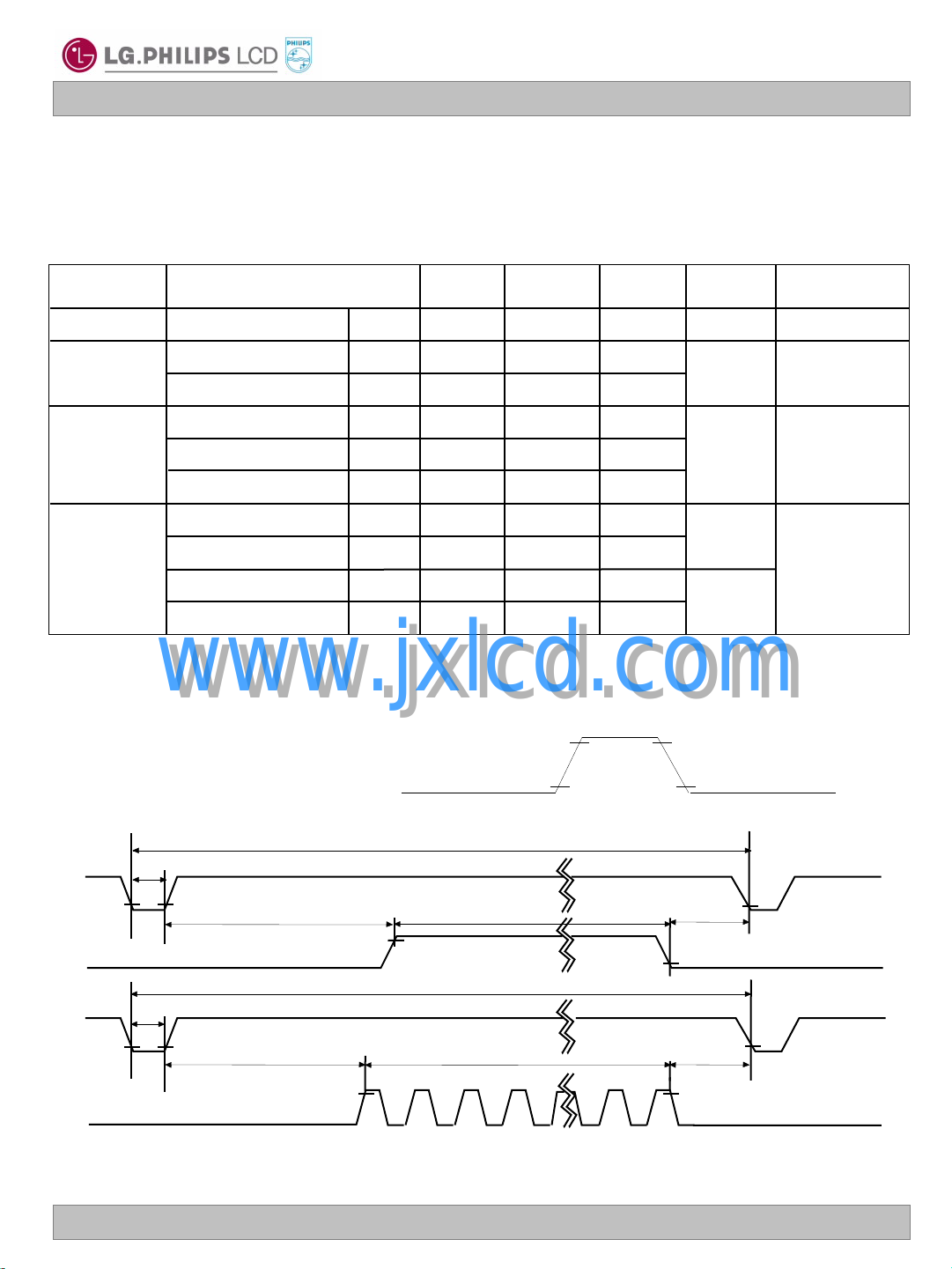
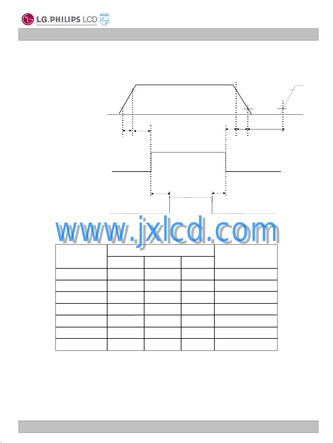
3-3. Signal Timing Specifications
This is the signal timing required at the input of the User connector. All of the interface signal timing should be
satisfied with the following specifications and specifications of LVDS Tx/Rx for it’s proper operation.
Table 5. TIMING TABLE
NoteUnitMaxTypMinSymbolITEM
Vsync
Data
Enable
3-4. Signal Timing Waveforms
Data Enable, Hsync, Vsync
www.jxlcd.com
www.jxlcd.com
fCLK FrequencyDCLK
tHPPeriodHsync
tWH Width
tVP Period
fvFrequency
tWV Width
tHBPHorizontal back porch
tHFPHorizontal front porch
tVBPVertical back porch
tVFPVertical front porch
High: 0.7VCC
Low: 0.3VCC
136413441206
-1368
830806780
606060
2461
-16010
-2410
-297
-31
MHz656565
tCLK
tHP
tCLK
tHP
Condition : VCC =3.3V
15.4ns
t
HP
Hsync
Date Enable
Vsync
Ver. 0.1 Oct. 1. 2004
t
WH
t
WV
Date Enable
t
VBP
t
HBP
tWHA
t
VP
tWVA
t
t
HFP
VFP
9 / 27
LP150X08
Liquid Crystal Display
Product Specification
3-5. Color Input Data Reference
The brightness of each primary color (red,green and blue) is based on the 6-bit gray scale data input for the
color ; the higher the binary input, the brighter the color. The table below provides a reference for color
versus data input.
Table 6. COLOR DATA REFERENCE
Input Color Data
Basic
Color
RED
GREEN
BLUE
Color
Black
Red
Green
Blue
Cyan
Magenta
Yellow
White
RED (00)
www.jxlcd.com
www.jxlcd.com
RED (01)
…
RED (62)
RED (63)
GREEN (00)
GREEN (01)
...
GREEN (62)
GREEN (63)
BLUE (00)
BLUE (01)
…
BLUE (62)
BLUE (63)
MSB LSB
RED
GREEN
MSB LSB
MSB LSB
B5 B4 B3 B2 B1 B0G5 G4 G3 G2 G1 G0R5 R4 R3 R2 R1 R0
BLUE
0 0 0 0 0 00 0 0 0 0 00 0 0 0 0 0
0 0 0 0 0 00 0 0 0 0 01 1 1 1 1 1
0 0 0 0 0 01 1 1 1 1 10 0 0 0 0 0
1 1 1 1 1 10 0 0 0 0 00 0 0 0 0 0
1 1 1 1 1 11 1 1 1 1 10 0 0 0 0 0
1 1 1 1 1 10 0 0 0 0 01 1 1 1 1 1
0 0 0 0 0 01 1 1 1 1 11 1 1 1 1 1
1 1 1 1 1 11 1 1 1 1 11 1 1 1 1 1
0 0 0 0 0 00 0 0 0 0 00 0 0 0 0 0
0 0 0 0 0 00 0 0 0 0 00 0 0 0 0 1
………
0 0 0 0 0 00 0 0 0 0 01 1 1 1 1 0
0 0 0 0 0 00 0 0 0 0 01 1 1 1 1 1
0 0 0 0 0 00 0 0 0 0 00 0 0 0 0 0
0 0 0 0 0 00 0 0 0 0 10 0 0 0 0 0
………
0 0 0 0 0 01 1 1 1 1 00 0 0 0 0 0
0 0 0 0 0 01 1 1 1 1 10 0 0 0 0 0
0 0 0 0 0 00 0 0 0 0 00 0 0 0 0 0
0 0 0 0 0 10 0 0 0 0 00 0 0 0 0 0
………
1 1 1 1 1 00 0 0 0 0 00 0 0 0 0 0
1 1 1 1 1 10 0 0 0 0 00 0 0 0 0 0
Ver. 0.1 Oct. 1. 2004
10 / 27
3-6. Power Sequence
LP150X08
Liquid Crystal Display
Product Specification
Power Supply For LCD
VCC
Interface Signal,
V
(LVDS Signal of Transmitter)
Power for Lamp
i
www.jxlcd.com
www.jxlcd.com
0V
90%
T
T
1
2
Valid Data
0V
T
3
Table 7. POWER SEQUENCE TABLE
Max.Typ.Min.
90%
10%10%
T
T
6
T
5
T
4
OFFOFF LAMP ON
UnitValueParameter
7
1
2
3
4
5
6
7
Notes : 1. Please avoid floating state of interface signal at invalid period.
2. When the interface signal is invalid, be sure to pull down the power
supply for LCD VCC to 0V.
3. Lamp power must be turn on after power supply for LCD and
interface signal are valid.
Ver. 0.1 Oct. 1. 2004
ms10--T
ms50-0T
ms--200T
ms--200T
ms50-0T
ms10-0T
ms--400T
11 / 27
LP150X08
Liquid Crystal Display
Product Specification
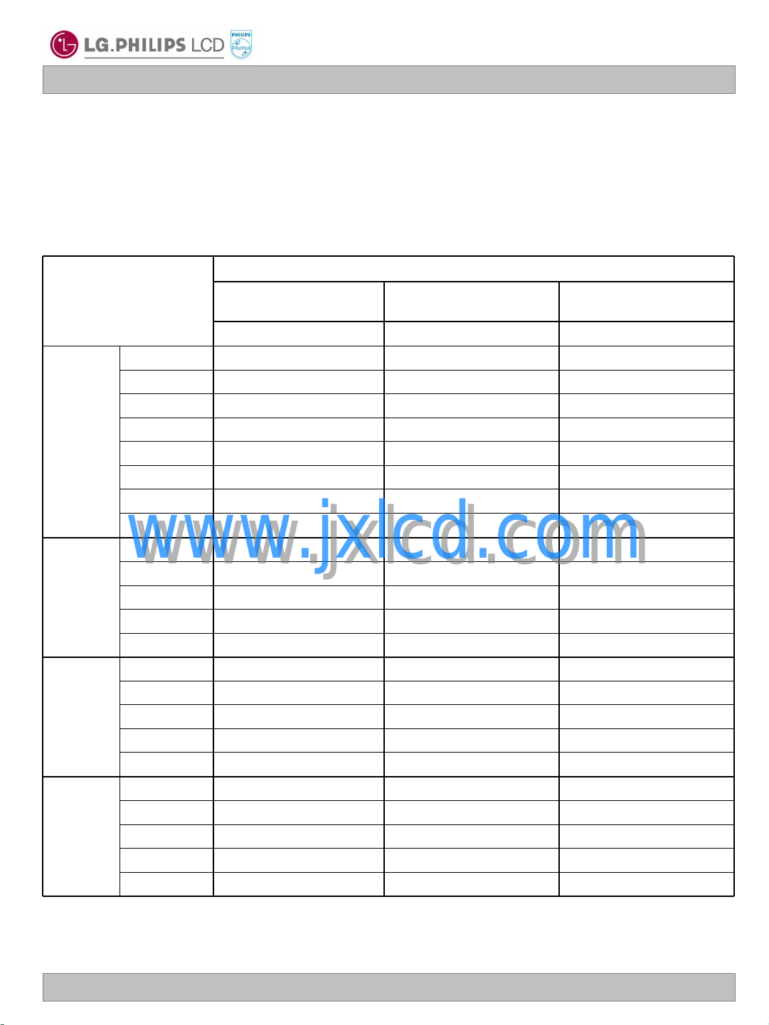
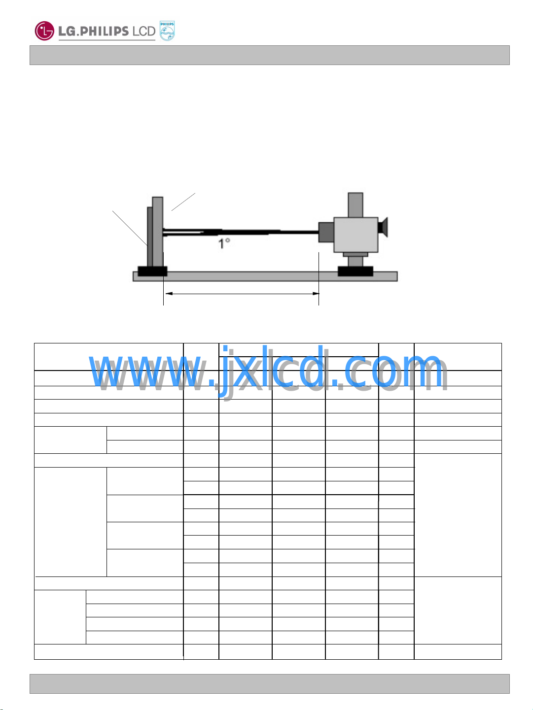
4. Optical Specification
Optical characteristics are determined after the unit has been ‘ON’ and stable for approximately 30 minutes in
a dark environment at 25C. The values specified are at an approximate distance 50cm from the LCD surface
at a viewing angle of and equal to 0.
FIG. 1 presents additional information concerning the measurement equipment and method.
FIG. 1 Optical Characteristic Measurement Equipment and Method
LCD ModuleOptical Stage(x,y) Pritchard 880 or
equivalent
50cm
Parameter Symbol NotesUnits
www.jxlcd.com
Surface Luminance, white (5P)
Luminance Variation (13P)
Color Coordinates
Viewing Angle
www.jxlcd.com
Rise Time
Decay Time
RED
GREEN
BLUE
x axis, right(=0) degree-4540r
x axis, left (=180)
y axis, up (=90)
y axis, down (=270)
Table 8. OPTICAL CHARACTERISTICS
Values
MaxTypMin
L
WH
WHITE
125
R
D
150
0.6170.5870.557RX
0.3730.3430.313RY
0.3510.3210.291GX
0.5600.5300.500GY
0.1890.1590.129BX
0.1700.1400.110BY
0.3430.3130.283WXWHITE
0.3590.3290.299WY
Ta=25C, VCC=3.3V, fV=60Hz
Dclk= 65MHz, IBL= 6.0mA
1-250175CRContrast Ratio
cd/m
ms2010-Tr
ms3020-Tr
degree-4540l
degree-1510u
degree-3530d
2
PR650 or equivalent
2
31.65--
4Response Time
5
6Gray Scale
Ver. 0.1 Oct. 1. 2004
12 / 27
 Loading...