

www.DataSheet.net/
Datasheet pdf - http://www.DataSheet4U.co.kr/
Product Specification
LP141XB
Liquid Crystal Display
www.jxlcd.com
www.jxlcd.com
Ver 0.1 MAR 20, 2001 Page 1/24
www.DataSheet.net/
Datasheet pdf - http://www.DataSheet4U.co.kr/
Product Specification
CONTENTS
NO. ITEM Page
- COVER 1
- CONTENTS 2
- RECORD OF REVISIONS 3
1 GENERAL DESCRIPTION 4
2 ABSOLUTE MAXIMUM RATINGS 5
3 ELECTRICAL SPECIFICATIONS 6
3-1 ELECTRICAL CHARACTERISTICS 6
3-2 INTERFACE CONNECTIONS 7
3-3 SIGNAL TIMING SPECIFICATIONS 9
LP141XB
Liquid Crystal Display
3-4 SIGNAL TIMING WAVEFORMS 10
3-5 COLOR INPUT DATA REFERENCE 11
3-6 POWER SEQUENCE 12
4 OPTICAL SPECIFICATIONS 13
5 MECHANICAL CHARACTERISTICS 14
6 RELIABILITY 18
7 INTERNATIONAL STANDARDS 19
7-1 SAFETY 19
7-2 EMC 19
8 PACKING 20
8-1 DESIGNATION OF LOT MARK 20
8-2 PACKING FORM 20
9 PRECAUTIONS 21
APPENDIX
A-1 OPTICAL CHARACTERISTIC MEASUREMENT EQUIPMENT AND METHOD 23
A-2 LUMINANCE 23
www.jxlcd.com
www.jxlcd.com
A-3 RESPONSE TIME 23
A-4 VIEWING ANGLE 24
Ver 0.1 MAR 20, 2001 Page 2/24
www.DataSheet.net/
Datasheet pdf - http://www.DataSheet4U.co.kr/
Product Specification
LP141XB
Liquid Crystal Display
RECORDS OF REVISIONS
Version No Date Page DESCRIPTION
0.0
0.1
OCT 1, 2000
MAR 20, 2001 - 4
6
7
13
14
www.jxlcd.com
www.jxlcd.com
18
First Draft
Change 1. General Description
Changed the luminance and weight
specifications.
Change 3-1. Electrical Characteristics
Defined the measurement condition about
the specificated rush current and duration of
rush current
Change 3-2. Interface Connections
Corrected the matching conncetor
Change 4. Optical Specifications
Defined CIE Color Coordinates and changed
the luminance Specifications.
Change 5. Mechanical Characteristics
Changed the weight specifications.
Change 6. Reliability
Corrected the environment test condition
20
(Altitude Operating)
Change 8-2. Packing Form
Added the box size.
Ver 0.1 MAR 20, 2001 Page 3/24
www.DataSheet.net/
Datasheet pdf - http://www.DataSheet4U.co.kr/
Product Specification
LP141XB
Liquid Crystal Display
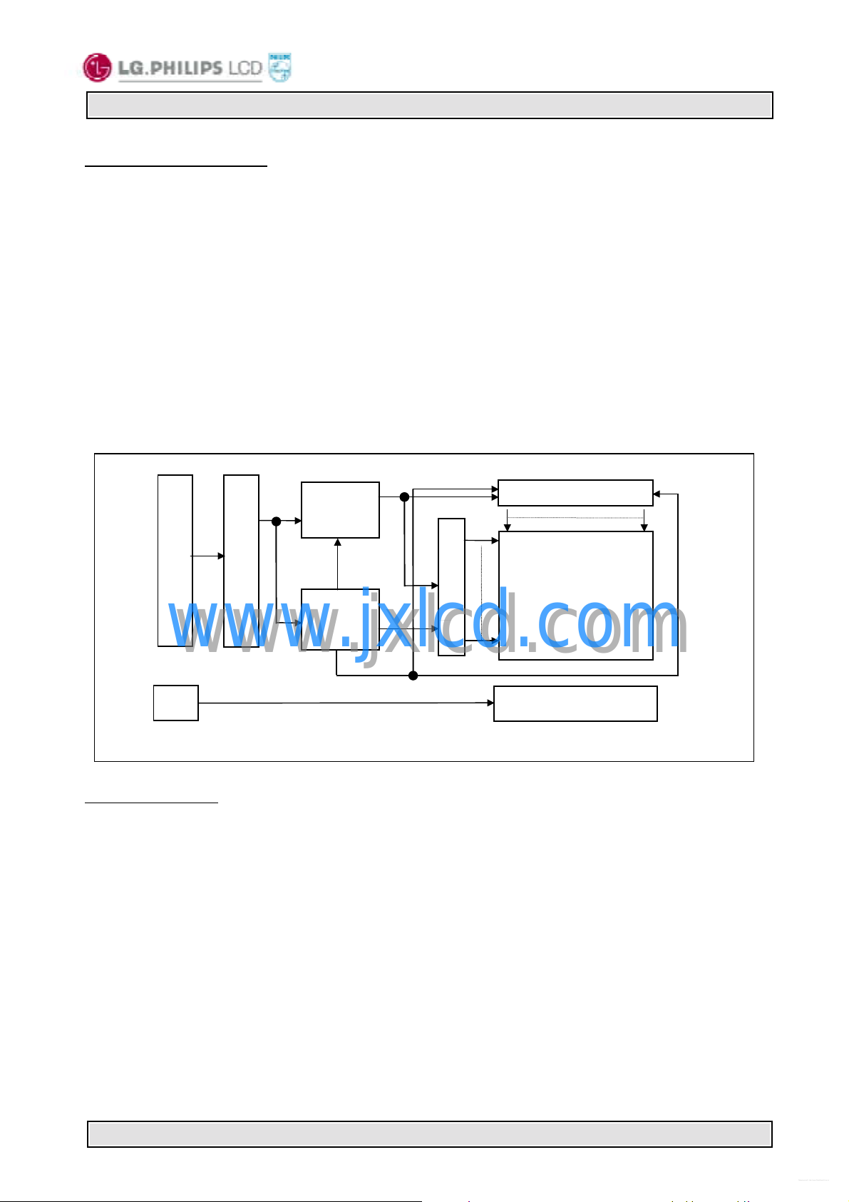
1. General Description
The LP141XB is a Color Active Matrix Liquid Crystal Display with an integral Cold Cathode Fluorescent
Lamp(CCFL) back light system. The m atrix employs a-Si Thin Film Transistor as the active elem ent. It is a
transmissive type display operating in the normally white mode. This TFT -LCD has a 14.1 inches diagonally
measured active display area with XGA resolution(768 vertical by 1024 horizontal pixel array). Each pixel is
divided into Red, Green and Blue sub-pixels or dots which ar e arranged in vertical str ipes. Gray scale or the
brightness of the sub-pixel color is determined with a 6-bit gray scale signal for each dot, thus, pres enting a
palette of more than 262,144 colors.
T he LP141XB has been designed to apply the interface method that enables low power, high speed, low EMI.
Flat Link must be used as a LVDS(Low Voltage Differential Signaling) chip.
The LP141XB is intended to support applications where thin thickness, low power are critical factors and
graphic displays are important. In com bination with the vertical arrangement of the sub-pix els, the LP141XB
characteristics provide an excellent flat panel display for office automation products such as Notebook PC.
Timing
Control
Block
Column driver circuit
CN1
FlatLink interface
www.jxlcd.com
www.jxlcd.com
CN2
Power
Block
Row Driver circuit
TFT-LCD
(1024×768)
Backlight Ass’y
General Features
Active screen size 14.1 inches(35.814cm) diagonal
Outline dimensions 298.5(H) × 227(V) × 5.5(D) mm (Typ.)
Pixel pitch 0.279 mm × 0.279 mm
Pixel format 1024 horiz. by 768 vert. pixels
RGB stripe arrangement
Color depth 6-bit, 262,144 colors
Luminance,White 170 cd/m
Power Consumption Total 4.65Watt(Typ.)
Weight 485g (Typ.)
Display operating mode Transmissive mode, normally white
Surface treatments Hard coating (3H),
Anti-glare treatment of the front polarizer
2
(Typ.)
Ver 0.1 MAR 20, 2001 Page 4/24
www.DataSheet.net/
Datasheet pdf - http://www.DataSheet4U.co.kr/
Product Specification
LP141XB
Liquid Crystal Display
2. Absolute Maximum Ratings
The following are maximum values which, if exceeded, may cause faulty operation or damage to the unit.
Table 1 ABSOLUTE MAXIMUM RATINGS
Parameter Symbol
Power Input Voltage
Operating Temperature
Storage Temperature
Operating Ambient Humidity
Storage Humidity
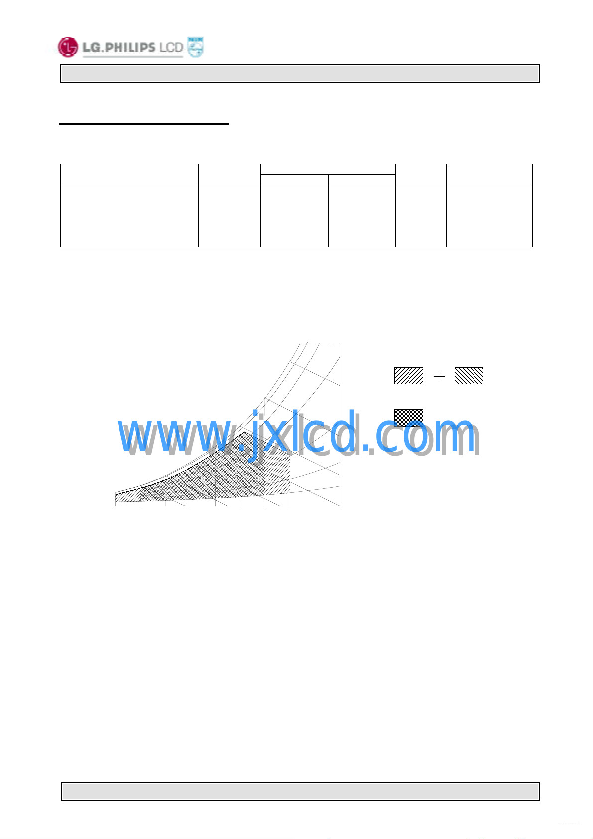
Note: 1. Temperature and relative humidity range are shown in the figure below.
Wet bulb temperature should be 39℃ Max, and no condensation of water.
V
CC
T
OP
T
ST
H
OP
H
ST
Values
Min. Max.
-0.3
0
-20
10
10
4.0
50
60
90
90
Units Notes
%RH
%RH
Vdc
℃
℃
at 25 ±5℃
1
1
1
1
Wet Bulb
Temperature [℃]
30
www.jxlcd.com
www.jxlcd.com
10
0
-20
10
Dry Bulb Temperature [℃]
20
20 30 40 50
40
50
60
60 70 80 0
95% 80%
60
40
20
10
%
%
%
Humidity [(%)RH]
%
Storage
Operation
Ver 0.1 MAR 20, 2001 Page 5/24
www.DataSheet.net/
Datasheet pdf - http://www.DataSheet4U.co.kr/
Product Specification
LP141XB
Liquid Crystal Display
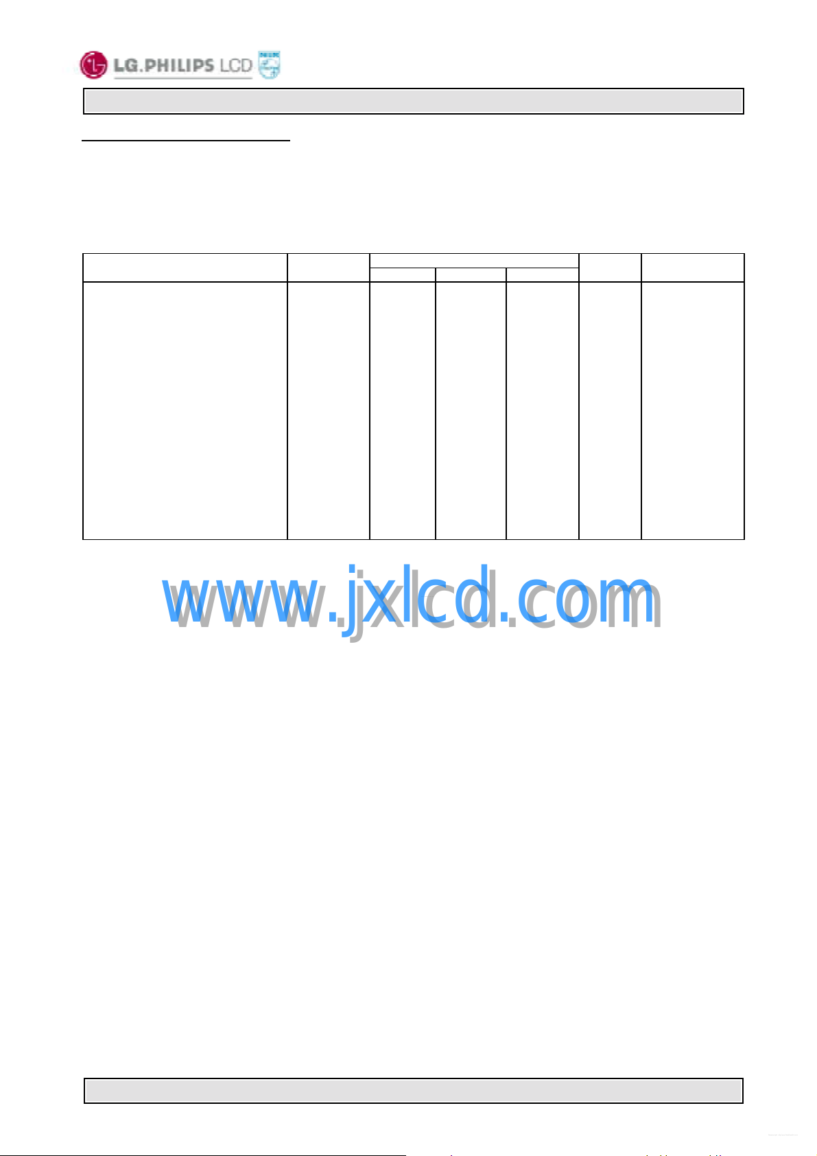
3. Electrical Specifications
3-1. Electrical Characteristics
The LP141XB requires two power inputs. One is employed to power the LCD electronics and to drive the
TFT array and liquid crystal. The second input which powers the CCFL, is typically generated by an inverter.
The inverter is an external unit to the LCD.
Table 2 ELECTRICAL CHARACTERISTICS:
Parameter Symbol Values Units Notes
Min. Typ. Max.
MODULE:
Power Supply Input Voltage
Power Supply Input Current
Differential Impedance
Power Consumption
Rush Current
Duration of rush current
LAMP
Operating Voltage
Operating Current
Established Starting Voltage
at 25℃
at 0℃
Operating Frequency
Discharge Stabilization Time
Power Consumption
Life Time
Note)The design of the inverter must have specifications for the lamp in LCD Assembly.
The performance of the Lamp in LCM, for example life time or brightness, is extremely influenced by the
characteristics of the DC-AC Inverter. So all the parameters of an inverter should be carefully designed
so as not to produce too much leakage current from high-voltage output of the inverter.
When you design or order the inverter, please make sure unwanted lighting caused by the mismatch
of the lamp and the inverter (no lighting, flicker, etc) never occurs. When you confirm it, the LCD
Assembly should be operated in the same condition as installed in your instrument.
Notes: 1. The specified current and power consumption are under the Vcc = 3.3V , 25℃, fv = 60Hz condition
whereas full black pattern is displayed and fv is the frame frequency.
2. This impedance value is needed to proper display and measured from LVDS Tx to the mating
connector.
3. The specified rush current and duration of rush current are under the Vcc = 3.3V,
Current limit = 1.6A, 25℃, fv = 60Hz condition whereas full black pattern is displayed and fv is the
frame frequency. The duration of rush current is about 20ms.
4. The variance of the voltage is ±10%.
5. The voltage above V
Otherwise, the lamps may not be turned on.
6. The output of the inverter must have symmetrical(negative and positive) voltage waveform and
symmetrical current waveform. (Unsymmetrical ratio is less than 10%) Please do not use the inverter
which has unsymmetrical voltage and unsymmetrical current and spike wave. Lamp frequency may
produce interference with horizontal synchronous frequency and as a result
this may cause beat on the display.
Therefore lamp frequency shall be as away as possible from the horizontal synchronous frequency
and from its harmonics in order to prevent interference.
7. Let’s define the brightness of the lamp after being lighted for 5 minutes as 100%.
Ver 0.1 MAR 20, 2001 Page 6/24
www.jxlcd.com
www.jxlcd.com
should be applied to the lamps for more than 1second for start-up.
s
V
I
Z
I
RUSH
T
RUSH
CC
CC
Pc
V
IL
V
F
T
PL
m
L
s
L
s
3.0
-
90
-
-
-
680(6mA)
3.0
-
-
45
-
10,000
3.3
0.310
100
1.02
1.0
-
725(5mA)
5.0
-
-
58
3.63
3.6
0.350
110
1.15
1.5
30
875(3mA)
6.0
1170
1450
80
3
4.08
-
Vdc
A
Ohm
W
A
ms
V
rms
mA
rms
V
rms
V
rms
kHz
Minutes
W
Hours
1
2
1
3
3
4
5
6
7
8
9
6mA
www.DataSheet.net/
Datasheet pdf - http://www.DataSheet4U.co.kr/
Product Specification
Ts is the time required for the brightness of the center of the lamp to be not less than 95%.
8. The lamp power consumption shown above does not include loss of external inverter.
The used lamp current is the lamp typical current.
9. The life time is determined as the time at which brightness of lamp is 50% compared to that of initial
value at the typical lamp current on condition of continuous operating at 25 ±2℃.
※ Do not attach a conducting tape to lamp connecting wire.
If the lamp wire attach to a conducting tape, TFT-LCD Module has a low luminance and the inverter
Has abnormal action. Because leakage current is occurred between lamp wire and conducting tape.
LP141XB
Liquid Crystal Display
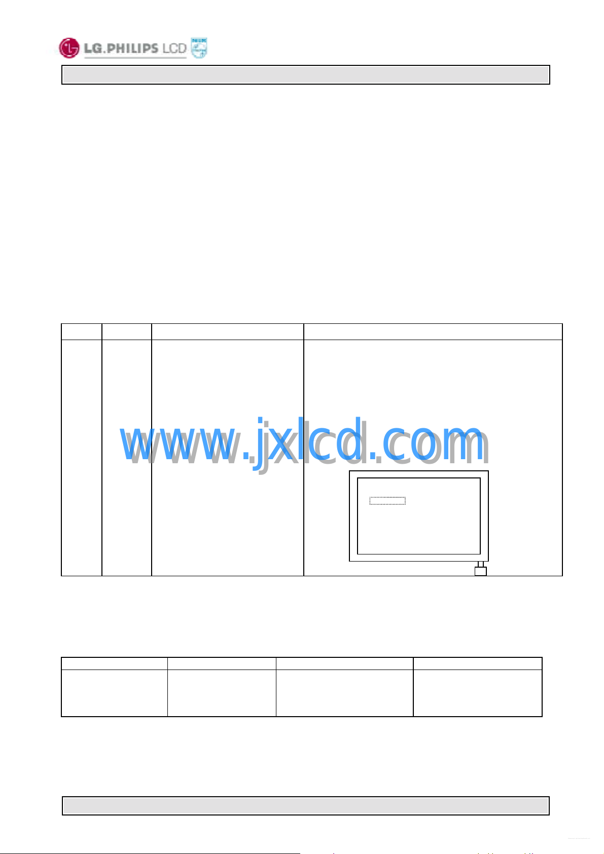
3-2. Interface Connections
This LCD employs two interface connections, a 20 pin connector is used f or the module electronics and the
other connector is used for the integral backlight system.
The electronics interface connector is a model GT122-20P-H13R manufactured by LG Cable. The pin
configuration for the connector is shown in the table below.
Pin Symbol Description Notes
1
2
3
4
5
6
7
8
9
10
11
12
13
14
15
16
17
18
19
20
The backlight interf ace connector is a m odel BHSR-02VS-1, m anufactured by JST. The mating connec tor
part number is SM02B-BHSS-1 or equivalent. The pin c onfiguration for the connector is shown in the table
below.
Notes: 1. The high voltage side terminal is colored pink. The low voltage side terminal is white.
Table 3 MODULE CONNECTOR PIN CONFIGURATION (LVDS) [CN1]
Vcc
Vcc
GND
GND
A0M
A0P
GND
A1M
A1P
GND
www.jxlcd.com
www.jxlcd.com
A2M
A2P
GND
CLKM
CLKP
GND
NC
NC
GND
GND
Pin Symbol Description Notes
1
2
Differential Signal
Differential Signal
Differential Signal
Differential Signal
Differential Signal
Differential Signal
Differential Signal
Differential Signal
No Connection
No Connection
Table 4 BACKLIGHT CONNECTOR PIN CONFIGURATION
Power (3.3V)
Power (3.3V)
Ground
Ground
Ground
Ground
Ground
Ground
Ground
Ground
HV
LV
1. Interface chips
1.1 LCD : SN75LVDS88B (TI)
(SN75LVDS86 core + Timing Controller)
1.2 System : SN75LVDS84(TI)
* Pin to Pin compatible with TI LVDS
2. Connector
2.1 LCD : GT122-20P-H13 R (LG Cable)
2.2 Mating : FI-SE20M (JAE) or compatible
2.3 Connector pin arrangement
Viewing on Display side
Power supply for lamp
(High voltage side)
Power supply for lamp
(Low voltage side)
1 … 20
CN1
CN2
1
1
Ver 0.1 MAR 20, 2001 Page 7/24
www.DataSheet.net/
Datasheet pdf - http://www.DataSheet4U.co.kr/
Product Specification
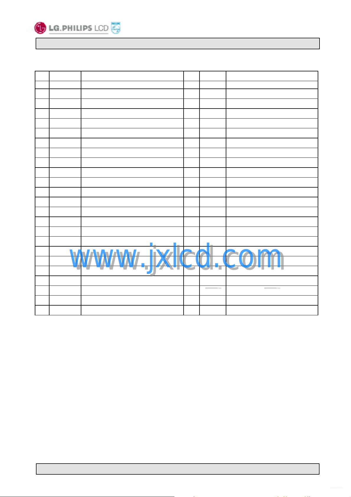
Table 5 REQUIRED SIGNAL ASSIGNMENT FOR FlatLink Transmitter
Pin # Pin Name Require Signals Pin # Pin Name Require Signals
1 D4 R4 48 D3 R3
2 Vcc Vcc 47 D2 R2
3 D5 R5 46 GND GND
4 D6 G0 45 D1 R1
5 GND GND 44 D0 R0
6 D7 G1 43 NC NC
7 D8 G2 42 LVDS GND LVDS GND
8 Vcc Vcc 41 Y0M A0M
9 D9 G3 40 Y0P A0P
10 D10 G4 39 Y1M A1M
11 GND GND 38 Y1P A1P
12 D11 G5 37 LVDS Vcc LVDS Vcc
13 D12 B0 36 LVDS GND LVDS GND
14 NC NC 35 Y2M A2M
15 D13 B1 34 Y2P A2P
16 D14 B2 33 CLKOUTM CLKM
17 GND GND 32 CLKOUTP CLKP
18 D15 B3 31 LVDS GND LVDS GND
19 D16 B4 30 PLLGND PLL GND
20 D17 B5 29 PLLVcc PLL Vcc
21 Vcc Vcc 28 PLLGND PLL GND
22 D18 HSYNC 27 SHDN SHDN
23 D19 VSYNC 26 CLKIN Dclk
24 GND GND 25 D20 DE(Data Enable)
www.jxlcd.com
www.jxlcd.com
LP141XB
Liquid Crystal Display
Notes : Refer to LVDS Transmitter Data Sheet for detail descriptions.
Ver 0.1 MAR 20, 2001 Page 8/24
 Loading...