


www.DataSheet.net/
Datasheet pdf - http://www.DataSheet4U.co.kr/
LG LCD Inc.
( ) Preliminary Specification
( ♦♦♦♦ ) Final Specification
LP141XA-A1NA
Liquid Crystal Display
Product Specification
SPECIFICATION
FOR
APPROVAL
Title 14.1” XGA TFT LCD
BUYER SUPPLIER LG LCD Inc.
MODEL MODEL LP141XA-A1NA
Please return 1 copy for your confirmation
with your signature and comments.
www.jxlcd.com
www.jxlcd.com
SIGNATURE
/
/
/
DATE
APPROVED BY
Y. K. Hwang / G.
Manager
REVIEWED BY
S. C. Yoon / Manager
B. H. Koo / Manager
PREPARED BY
H. S. Song / Engineer
S. J. Lee / Engineer
Product Engineering Dept.
LG LCD Inc.
DATE
Ver 1.0 JUL. 06, 1999 Page 1/25
www.DataSheet.net/
Datasheet pdf - http://www.DataSheet4U.co.kr/
LG LCD Inc.
Product Specification
LP141XA-A1NA
Liquid Crystal Display
CONTENTS
NO. ITEM Page
- COVER 1
- CONTENTS 2
- RECORD OF REVISIONS 3
1 GENERAL DESCRIPTION 4
2 ABSOLUTE MAXIMUM RATINGS 5
3 ELECTRICAL SPECIFICATIONS 6
3-1 ELECTRICAL CHARACTERISTICS 6
3-2 INTERFACE CONNECTIONS 7
3-3 SIGNAL TIMING SPECIFICATIONS 9
3-4 SIGNAL TIMING WAVEFORMS 10
3-5 COLOR INPUT DATA REFERENCE 11
3-6 POWER SEQUENCE 12
3-7 Vcc DIP CONDITION 13
4 OPTICAL SPECIFICATIONS 14
5 MECHANICAL CHARACTERISTICS 15
6 RELIABILITY 19
7 INTERNATIONAL STANDARDS 20
7-1 SAFETY 20
7-2 EMC 20
8 PACKING 21
8-1 DESIGNATION OF LOT MARK 21
8-2 PACKING FORM 21
9 PRECAUTIONS 22
APPENDIX
www.jxlcd.com
www.jxlcd.com
A-1 OPTICAL CHARACTERISTIC MEASUREMENT EQUIPMENT AND METHOD 24
A-2 LUMINANCE 24
A-3 RESPONSE TIME 24
A-4 VIEWING ANGLE 25
Ver 1.0 JUL. 06, 1999 Page 2/25
www.DataSheet.net/
Datasheet pdf - http://www.DataSheet4U.co.kr/
Version No Date Page DESCRIPTION
LG LCD Inc.
Product Specification
RECORDS OF REVISIONS
LP141XA-A1NA
Liquid Crystal Display
1.0
Jul. 06, 1999
www.jxlcd.com
www.jxlcd.com
First Draft and modified Color Coordinates from LP141XA-A1
-
14
Changed Color Coordinates
Min. Typ Max Min. Typ Max
Rx 0.548 0.578 0.608 0.550 0.580 0.610
Ry 0.317 0.347 0.377 0.323 0.353 0.383
Gx 0.278 0.308 0.338 0.280 0.310 0.340
Gy 0.507 0.537 0.567 0.518 0.548 0.578
Bx 0.121 0.151 0.181 0.122 0.152 0.182
By 0.101 0.131 0.161 0.110 0.140 0.170
Wx 0.281 0.311 0.341 0.287 0.317 0.347
Wy 0.311 0.341 0.371 0.324 0.354 0.384
Ver 1.0 JUL. 06, 1999 Page 3/25
www.DataSheet.net/
Datasheet pdf - http://www.DataSheet4U.co.kr/
LG LCD Inc.
Product Specification
LP141XA-A1NA
Liquid Crystal Display
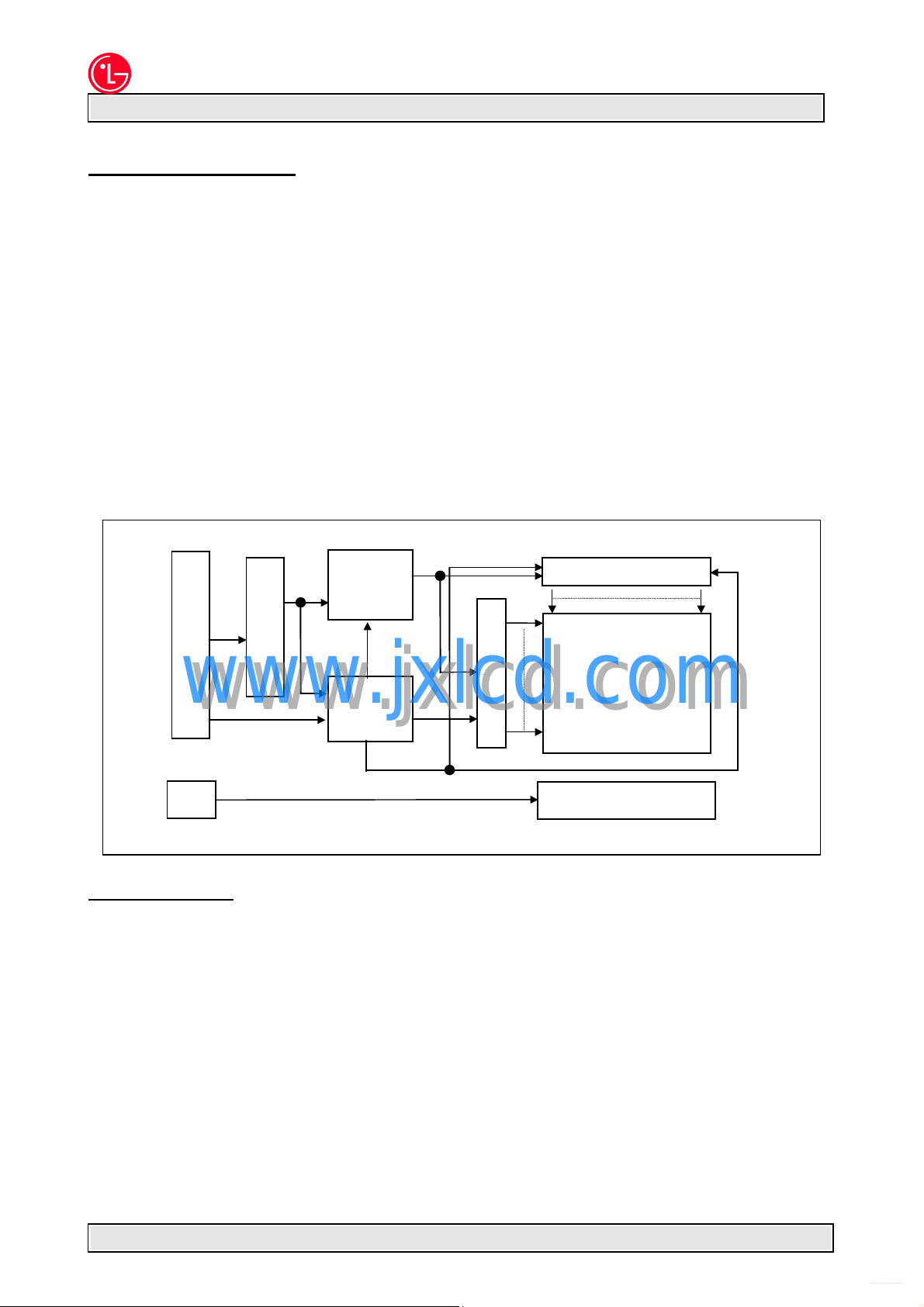
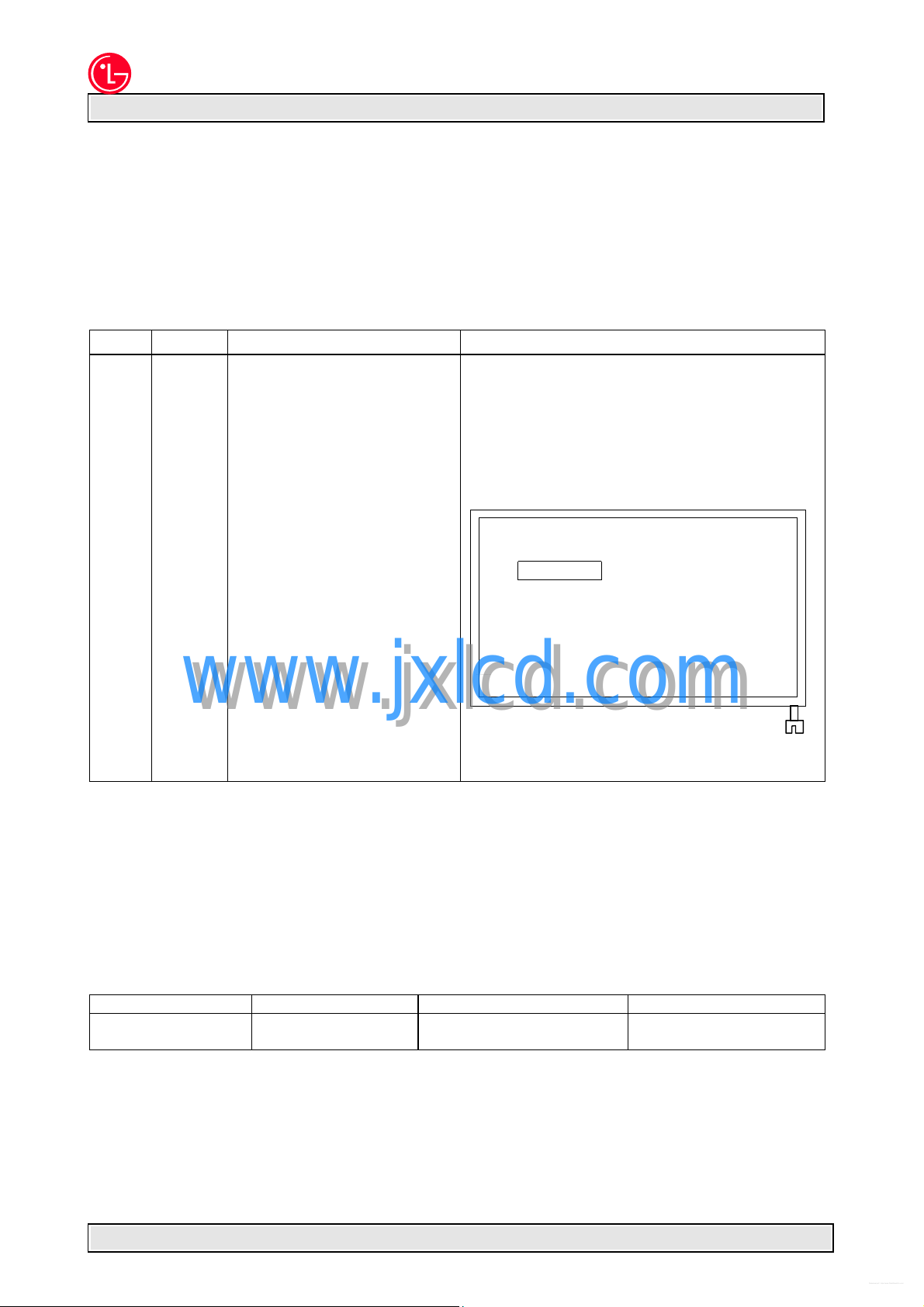
1. General Description
The LP141XA-A1NA is a Color Active Matrix Liquid Crystal Display with an integral Cold Cathode Fluorescent
Lamp(CCFL) back light system. The matrix employs a-Si Thin Film Transistor as the active element. It is a
transmissive type display operating in the normally white mode. This TFT-LCD has a 14.1 inch diagonally
measured active display area with XGA resolution(768 vertical by 1024 horizontal pixel array). Each pixel is
divided into Red, Green and Blue sub-pixels or dots which are arranged in vertical stripes. Gray scale or the
brightness of the sub-pixel color is determined with a 6-bit gray scale signal for each dot, thus, presenting a
palette of more than 262,144 colors.
The LP141XA-A1NA has been designed to apply the interface method that enables low power, high speed
low EMI. Flat Link must be used as a LVDS(Low Voltage Differential Signaling) chip.
The LP141XA-A1NA is intended to support applications where thin thickness, low power are critical factors
and graphic displays are important. In combination with the vertical arrangement of the sub-pixels, the
LP141XA-A1NA characteristics provide an excellent flat panel display for office automation products such as
Notebook PC.
Timing
Control
Block
CN1
FlatLink interface
www.jxlcd.com
www.jxlcd.com
CN2
Power
Block
Row Driver circuit
Column driver circuit
TFT-LCD
(1024×768)
Backlight Ass’y
General Features
Active screen size 14.1 inches(33.78cm) diagonal
Outline dimensions 298.5(H) 227.5(V) 5.8(D) mm (typ)
Pixel pitch 0.279 mm 0.279 mm
Pixel format 1024 horiz. By 768 vert. pixels
RGB stripe arrangement
Color depth 6-bit, 262,144 colors
Luminance, White 120 cd/m
Power Consumption Total 4.97Watt(typ)
Weight 580g (typ)
Display operating mode transmissive mode, normally white
Surface treatments hard coating(3H),
anti-glare treatment of the front polarizer
2
(typ)
Ver 1.0 JUL. 06, 1999 Page 4/25
www.DataSheet.net/
Datasheet pdf - http://www.DataSheet4U.co.kr/
LG LCD Inc.
Product Specification
LP141XA-A1NA
Liquid Crystal Display
2. Absolute Maximum Ratings
The following are maximum values which, if exceeded, may cause faulty operation or damage to the unit.
Table 1 ABSOLUTE MAXIMUM RATINGS
Parameter symbol
Power Input Voltage
Operating Temperature
Storage Temperature
Note: 1. Temperature and relative humidity range are shown in the figure below.
V
CC
TOP
T
ST
Values
Min. Max.
-0.3
0
-20
+3.6
+50
+60
Units Notes
Vdc
at 25
1
1
Relative Humidity (% RH)
-40
100
90
80
Operating Range
60
40
www.jxlcd.com
www.jxlcd.com
20
Storage Range
5
0
Temperature
60 40 20 -20
80
3. Electrical Specifications
Ver 1.0 JUL. 06, 1999 Page 5/25
www.DataSheet.net/
Datasheet pdf - http://www.DataSheet4U.co.kr/
LG LCD Inc.
Product Specification
LP141XA-A1NA
Liquid Crystal Display
3-1. Electrical Characteristics
The LP141XA-A1NA requires two power inputs. One is employed to power the LCD electronics and to drive
the TFT array and liquid crystal. The second input which powers the CCFL, is typically generated by an
inverter. The inverter is an external unit to the LCD.
Table 2 ELECTRICAL CHARACTERISTICS:
Values
Min. Typ. Max.
MODULE:
Power Supply Input Voltage
Power Supply Input Current
Differential Impedance
Power Consumption
Rush current
LAMP
Operating Voltage
Operating Current
Established Starting Voltage
at 25
at 0
Operating Frequency
Power Consumption
Life Time
Notes: 1. The specified current and power consumption are under the Vcc = 3.3V , 25, fv = 60Hz condition
whereas Black pattern is displayed.
2. This impedance value is needed to proper display and measured form LVDS Tx to the mating
connector.
3. The duration of rush current is about 20ms.
4. The variance of the voltage is 10%.
6. The lamp power consumption shown above does not include loss of external inverter.
7. The life time is determined as the time at which brightness of lamp is 50% compare to that of initial
www.jxlcd.com
www.jxlcd.com
5. The transformer output voltage in the inverter must be high considering to the loss of the ballast
capacitor in the inverter.
value at the typical lamp current
V
I
CC
Zm
P
I
RUSH
V
IBL
f
BL
PBL
CC
c
BL
3.0
-
90
-
-
680
3.0
-
-
40
-
10,000
3.3
0.410
100
1.35
1.5
725
5.0
-
-
60
3.63
15,000
3.6
0.570
110
1.88
1.8
850
6.0
1170
1450
80
4.08
-
Vdc
A
ohm
Watts
A
V
RMS
mA
V
RMS
V
RMS
kHz
Watts
Hrs
Notes Units Symbol Parameter
1
2
1
3
4
5
6
7
Ver 1.0 JUL. 06, 1999 Page 6/25
www.DataSheet.net/
Datasheet pdf - http://www.DataSheet4U.co.kr/
LG LCD Inc.
Product Specification
LP141XA-A1NA
Liquid Crystal Display
3-2. Interface Connections
This LCD employs two interface connections, a 20 pin connector is used for the module electronics and the
other connector is used for the integral backlight system.
The electronics interface connector is a model FI-SEB-20P-HF manufactured by JAE or equivalent. The pin
configuration for the connector is shown in the table below.
Pin Symbol Description Notes
1
2
3
4
5
6
7
8
9
10
11
12
13
14
15
16
17
18
19
20
The backlight interface connector is a model BHSR-02VS-1, manufactured by JST. The mating connector
part number is SM02B-BHSS-1 or equivalent. The pin configuration for the connector is shown in the table
below.
Notes: 1. The high voltage input terminal is colored white.
2. The low voltage input terminal is colored black.
Table 3 MODULE CONNECTOR PIN CONFIGURATION (LVDS) [CN1]
VCC
VCC
GND
GND
A0M
A0P
GND
A1M
A1P
GND
A2M
A2P
GND
CLKM
CLKP
GND
NC
NC
GND
GND
www.jxlcd.com
www.jxlcd.com
Table 4 BACKLIGHT CONNECTOR PIN CONFIGURATION [CN2]
Pin Symbol Description Notes
1
2
Difference Signal
Difference Signal
Difference Signal
Difference Signal
Difference Signal
Difference Signal
Difference Signal
Difference Signal
No Connection
No Connection
Power (3.3V)
Power (3.3V)
Ground
Ground
Ground
Ground
Ground
Ground
Ground
Ground
HV
LV
1. Interface chips
1.1 LCD : FD85310(National Semiconductor)
2. Connector
2.1 LCD : 15021-2040R(UJU Electronics)
2.2 Mating : FI-WEB21P-HF(JAE)
2.3 Connector pin arrangement
High voltage input
Low voltage input
No. 1
CN1
Viewing on Display side
20
1
2
CN2
Ver 1.0 JUL. 06, 1999 Page 7/25
www.DataSheet.net/
Datasheet pdf - http://www.DataSheet4U.co.kr/
LG LCD Inc.
Product Specification
Table 5 REQUIRED SIGNAL ASSIGNMENT FOR FlatLink Transmitter
Pin # Pin Name Require Signals Pin # Pin Name Require Signals
1 D4 R4 48 D3 R3
2 Vcc Vcc 47 D2 R2
3 D5 R5 46 GND GND
4 D6 G0 45 D1 R1
5 GND GND 44 D0 R0
6 D7 G1 43 NC NC
7 D8 G2 42 LVDS GND LVDS GND
8 Vcc Vcc 41 Y0M A0M
9 D9 G3 40 Y0P A0P
10 D10 G4 39 Y1M A1M
11 GND GND 38 Y1P A1P
12 D11 G5 37 LVDS Vcc LVDS Vcc
13 D12 B0 36 LVDS GND LVDS GND
14 NC NC 35 Y2M A2M
15 D13 B1 34 Y2P A2P
16 D14 B2 33 CLKOUTM CLKM
17 GND GND 32 CLKOUTP CLKP
18 D15 B3 31 LVDS GND LVDS GND
19 D16 B4 30 PLLGND PLL GND
20 D17 B5 29 PLLVcc PLL Vcc
21 Vcc Vcc 28 PLLGND PLL GND
22 D18 HSYNC 27 SHDN SHDN
23 D19 VSYNC 26 CLKIN Dclk
24 GND GND 25 D20 DE(Data Enable)
www.jxlcd.com
www.jxlcd.com
LP141XA-A1NA
Liquid Crystal Display
Notes : Refer to LVDS Transmitter Data Sheet for detail descriptions.
Ver 1.0 JUL. 06, 1999 Page 8/25
 Loading...