

LP141X8(A1M3)
www.DataSheet.net/
Datasheet pdf - http://www.DataSheet4U.co.kr/
Liquid Crystal Display
Product Specification
SPECIFICATION
FOR
APPROVAL
)
(
(
Preliminary Specification
)
Final SpecificationV
14.1” XGA TFT LCDTitle
DELLBUYER
MODEL
*When you obtain standard approval,
www.jxlcd.com
www.jxlcd.com
DATESIGNATURE
/
/
/
please use the above model name without suffix
S.H. Kang / G.Manager
REVIEWED BY
J.H. Park / Manager
S.M. Lee / Manager
PREPARED BY
W.Y. Park / Engineer
B.D. Jun / Engineer
LG.Philips LCD Co., Ltd.SUPPLIER
LP141X8*MODEL
A1M3Suffix
DATESIGNATURE
Please return 1 copy for your confirmation with
your signature and comments.
Ver. 1.0 DEC. 20, 2002
Products Engineering Dept.
LG. Philips LCD Co., Ltd
1 / 29
Product Specification
www.DataSheet.net/
Datasheet pdf - http://www.DataSheet4U.co.kr/
Contents
LP141X8(A1M3)
Liquid Crystal Display
ITEMNo
COVER
CONTENTS
RECORD OF REVISIONS
GENERAL DESCRIPTION1
ABSOLUTE MAXIMUM RATINGS2
ELECTRICAL SPECIFICATIONS3
ELECTRICAL CHARACTREISTICS3-1
INTERFACE CONNECTIONS3-2
SIGNAL TIMING SPECIFICATIONS3-3
SIGNAL TIMING WAVEFORMS3-4
COLOR INPUT DATA REFERNECE3-5
www.jxlcd.com
www.jxlcd.com
POWER SEQUENCE3-6
OPTICAL SFECIFICATIONS4
MECHANICAL CHARACTERISTICS5
Page
1
2
3
4
5
6
7
9
9
10
11
12
16
RELIABLITY6
INTERNATIONAL STANDARDS7
SAFETY7-1
EMC7-2
PACKING8
DESIGNATION OF LOT MARK8-1
PACKING FORM8-2
PRECAUTIONS9
APPENDIX. Enhanced Extended Display Identification Data A
APPENDIX. Inspection CriteriaB
Ver. 1.0 DEC. 20, 2002
20
21
21
22
22
23
25
28
2 / 29

Product Specification
www.DataSheet.net/
Datasheet pdf - http://www.DataSheet4U.co.kr/
RECORD OF REVISIONS
LP141X8(A1M3)
Liquid Crystal Display
DescriptionPageRevision DateRevision No
Final -DEC.20.20021.0
www.jxlcd.com
www.jxlcd.com
Note
Ver. 1.0 DEC. 20, 2002
3 / 29
LP141X8(A1M3)
www.DataSheet.net/
Datasheet pdf - http://www.DataSheet4U.co.kr/
Liquid Crystal Display
Product Specification
1. General Description
The LP141X8(A1M3) is a Color Active Matrix Liquid Crystal Display with an integral Cold Cathode
Fluorescent Lamp (CCFL) backlight system. The matrix employs a-Si Thin Film Transistor as the active
element. It is a transmissive type display operating in the normally white mode. This TFT-LCD has 14.1
inches diagonally measured active display area with XGA resolution(768 vertical by 1024 horizontal pixel
array). Each pixel is divided into Red, Green and Blue sub-pixels or dots which are arranged in vertical
stripes. Gray scale or the brightness of the sub-pixel color is determined with a 6-bit gray scale signal for
each dot, thus, presenting a palette of more than 262,144 colors.
The LP141X8(A1M3) has been designed to apply the interface method that enables low power, high speed,
low EMI.
The LP141X8(A1M3) is intended to support applications where thin thickness, low power are critical factors
and graphic displays are important. In combination with the vertical arrangement of the sub-pixels, the
LP141X8(A1M3) characteristics provide an excellent flat display for office automation products such as
Notebook PC.
www.jxlcd.com
www.jxlcd.com
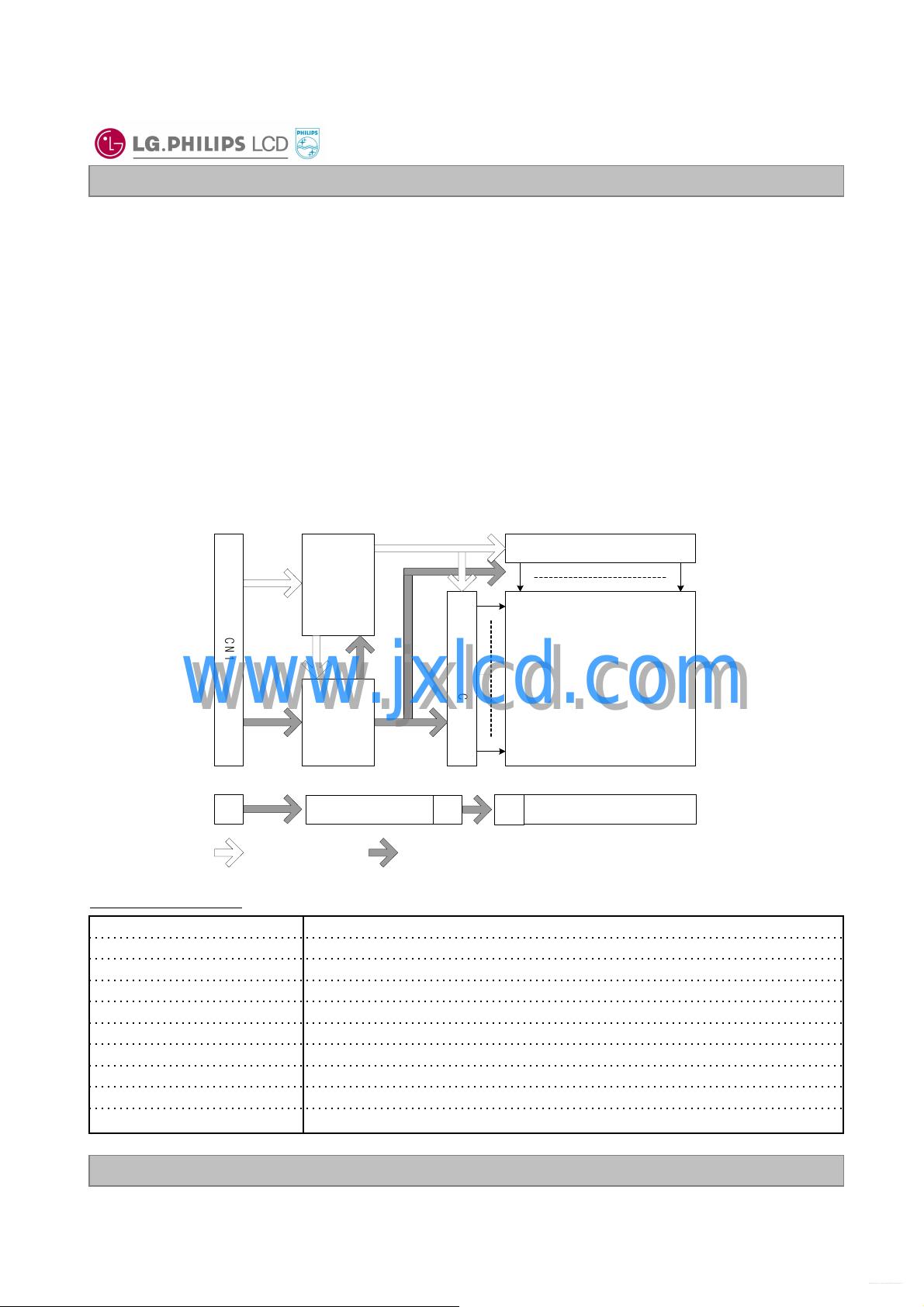
J1
General Features
LV D S
&
Tim ing
C o ntro l
B lock
C
N
1
P o w er
B lock
B /L Inverter
:C o n tro l & D ata :P o w er
14.1 inches(35.814cm) diagonal Active Screen Size
299(H) × 227(V) × 5.7(D) mm (Typ.)Outline Dimension
0.279 mm × 0.279 mm Pixel Pitch
1024 horiz. By 768 vert. Pixels RGB strip arrangementPixel Format
6-bit, 262,144 colorsColor Depth
150 cd/m2(Typ.)Luminance, White
Total 6.02 Watt(Typ.) @ LCM circuit 1.12Watt(Typ.), B/L input 4.9Watt(Typ.)Power Consumption
509 g (Typ.) w/o inverter and bracket, 521g(Max.) w/ inverter and bracketWeight
Transmissive mode, normally whiteDisplay Operating Mode
Hard coating(3H) Anti-glare treatment of the front polarizerSurface Treatment
C o lu m n D river C ircu it
C
J2
J3
TF T - LC D
(1 0 24 X 76 8 )
B ac klig ht A ss'y
Ver. 1.0 DEC. 20, 2002
4 / 29
LP141X8(A1M3)
www.DataSheet.net/
Datasheet pdf - http://www.DataSheet4U.co.kr/
Liquid Crystal Display
Product Specification
2. Absolute Maximum Ratings
The following are maximum values which, if exceeded, may cause faulty operation or damage to the unit.
Table 1. ABSOLUTE MAXIMUM RATINGS
60
Values
90% 80%
MaxMin
60
40
20
10
%
%
%
%
Parameter Notes
Power Input Voltage
Operating Temperature
Storage Temperature
Operating Ambient Humidity
Storage Humidity
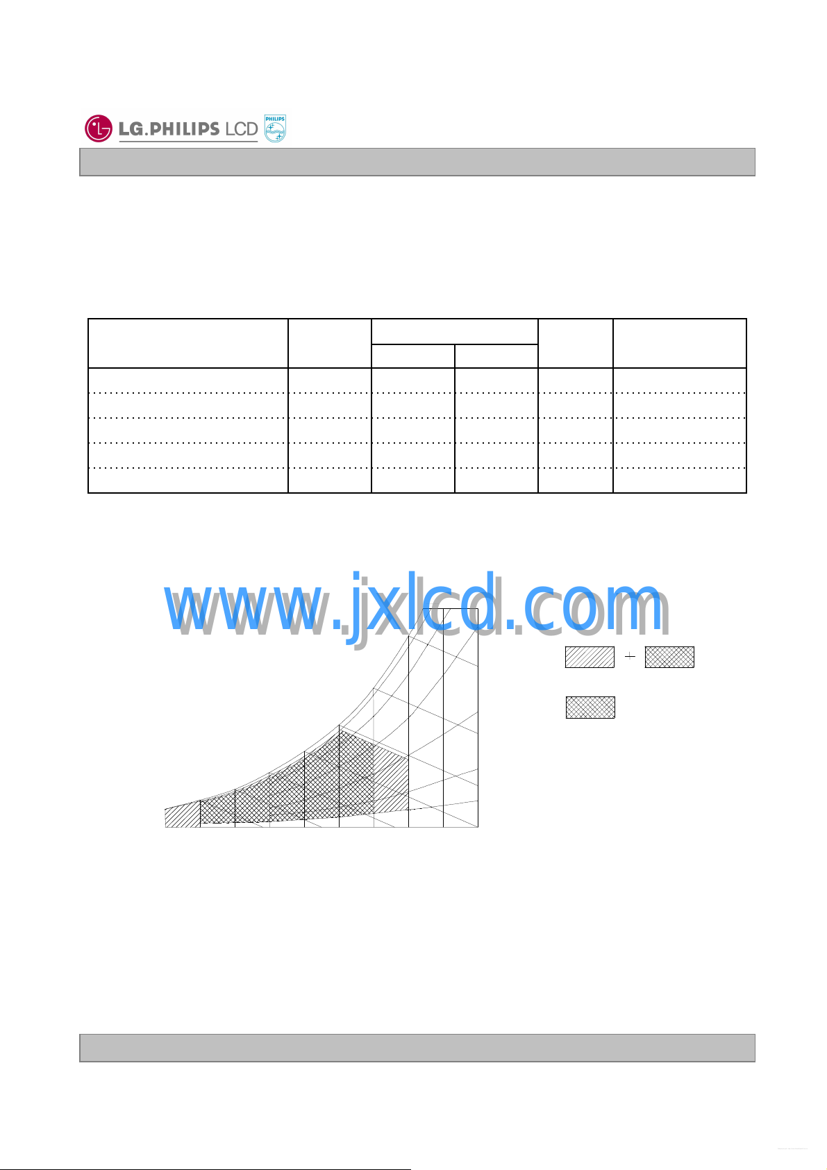
Note : 1. Temperature and relative humidity range are shown in the figure below.
Wet bulb temperature should be 39°CMax, and no condensation of water.
www.jxlcd.com
www.jxlcd.com
Wet Bulb
Temperature [℃℃℃℃]
20
10
0
Symbol
OP
ST
OP
ST
50
40
30
Units
Humidity[(%)RH]
Storage
Operation
at 25 ± 5°CVdc4.0-0.3VCC
1°C500T
1°C60-20H
1%RH9010H
1%RH9010H
-20
Ver. 1.0 DEC. 20, 2002
10
20 30 40 50
Dry Bulb Temperature [℃℃℃℃]
60 70 800
5 / 29

LP141X8(A1M3)
www.DataSheet.net/
Datasheet pdf - http://www.DataSheet4U.co.kr/
Liquid Crystal Display
Product Specification
3. Electrical Specifications
3-1. Electrical Characteristics
The LP141X8(A1M3) requires two power inputs. One is employed to power the LCD electronics and to
drive the TFT array and liquid crystal. The second input which powers the CCFL, is typically generated by an
inverter. The inverter is an external unit to the LCD.
Table 2. ELECTRICAL CHARACTERISTICS
Parameter Symbol
MODULE :
Power Supply Input Current
Differential Impedance
LAMP :
Operating Voltage
Operating Current
Operating Frequency
INVERTER :
Input Voltage
Input Current
Input Power Consumption
Output Voltage
Output Power Consumption
Open Lamp Voltage
Striking Time
www.jxlcd.com
www.jxlcd.com
OUT
OUT
CC
Zm
BL
BL
BL
IN
IN
IN
OUT
_FFOutput Current (Aging 30minutes)
_00
OUT
OPEN
S
Values
DC
RMS
DC
DC
DC
-00_H-FF_HBacklight Adjust (IBLControl)
RMS
RMS
NotesUnit
1mA375340-I
1Watt1.241.12-PcPower Consumption
2Ohm11010090
3mA
4Min3--TsDischarge Stabilization Time
5Hrs--10,000Life Time
6mA390340-I
6W5.624.904.17P
6V
7mA
7mA
7KHz756045Freq.Operating Frequency
6W4.523.943.36P
8V
9%--75ηEfficiency
10sec1.41.00.6T
MaxTypMin
3.63.33.0VCCPower Supply Input Voltage
910(2.7mA)725(5mA)680(6mA)V
6.05.02.7I
21.014.49.0V
5.25-2.0FPVEE_HighBacklight On/Off Control
0.8--0.3FPVEE_Low
780680580V
2.32.0-I
6.05.85.3I
--1450V
V
V
RMS
kHz805845f
V
V
V
RMS
RMS
Note)
1. The specified current and power consumption are under the Vcc = 3.3V , 25℃, fv = 60Hz condition
whereas full black pattern is displayed and fv is the frame frequency.
2. This impedance value is needed to proper display and measured form LVDS Tx to the mating connector.
3. The typical operating current is for the typical surface luminance (LWH) in optical characteristics.
Ver. 1.0 DEC. 20, 2002
6 / 29
LP141X8(A1M3)
www.DataSheet.net/
Datasheet pdf - http://www.DataSheet4U.co.kr/
Liquid Crystal Display
Product Specification
Note)
4. Define the brightness of the lamp after being lighted for 5 minutes as 100%, Ts is the time required for
the brightness of the center of the lamp to be not less than 95%.
5. The life time is determined as the time at which brightness of lamp is 50% compare to that of initial value
at the typical lamp current.
6. VIN= 14.4V, I
7. VIN= 9 ~ 21V.
8. No Load, VIN= 9V.
9. VIN=9V, 00_H.
10. No Load, VIN= 9 ~ 21V, 00_H
OUT
= 5.8mA.
3-2. Interface Connections
This LCD employs two interface connections, a 20 pin connector is used for the module electronics interface
and the other connector is used for the integral backlight system.
The electronics interface connector is a model GT122-20P-H15-R manufactured by LG Cable.
Table 3. MODULE CONNECTOR PIN CONFIGURATION (CN1)
17
19
20
VCC
EDID
Power Supply, 3.3V Typ.1
Power Supply, 3.3V Typ.VCC2
GroundGND3
www.jxlcd.com
www.jxlcd.com
GroundGND4
Negative LVDS differential data input (R0~R5,G0)RIN0-5
Positive LVDS differential data input (R0~R5,G0)RIN0+6
GroundGND7
Negative LVDS differential data input (G1~G5,B0~B1)RIN1-8
Positive LVDS differential data input (G1~G5,B0~B1)RIN1+9
GroundGND10
Negative LVDS differential data input (B2~B5,HS,VS,DE)RIN2-11
Positive LVDS differential data input (B2~B5,HS,VS,DE)RIN2+12
GroundGND13
Clock -CLK-14
Clock +CLK+15
GroundGND16
Power for EDIDV
ReservedNC18
Clock for EDIDCLK
EDID
EDID dataDATA
EDID
[LVDS Transmitter]
TI, SN75LVDS84 or equivalent
[LVDS Receiver]
TI, SN75LVDS88B
[Connector]
LCD: GT122-20P-H15-R, LG Cable
Mating : FI-SE20M, JAE or compatibles
[Connector pin arrangement]
LCD module rear view
20
NotesDescriptionSymbolPin
1
Ver. 1.0 DEC. 20, 2002
7 / 29
Product Specification
www.DataSheet.net/
Datasheet pdf - http://www.DataSheet4U.co.kr/
LP141X8(A1M3)
Liquid Crystal Display
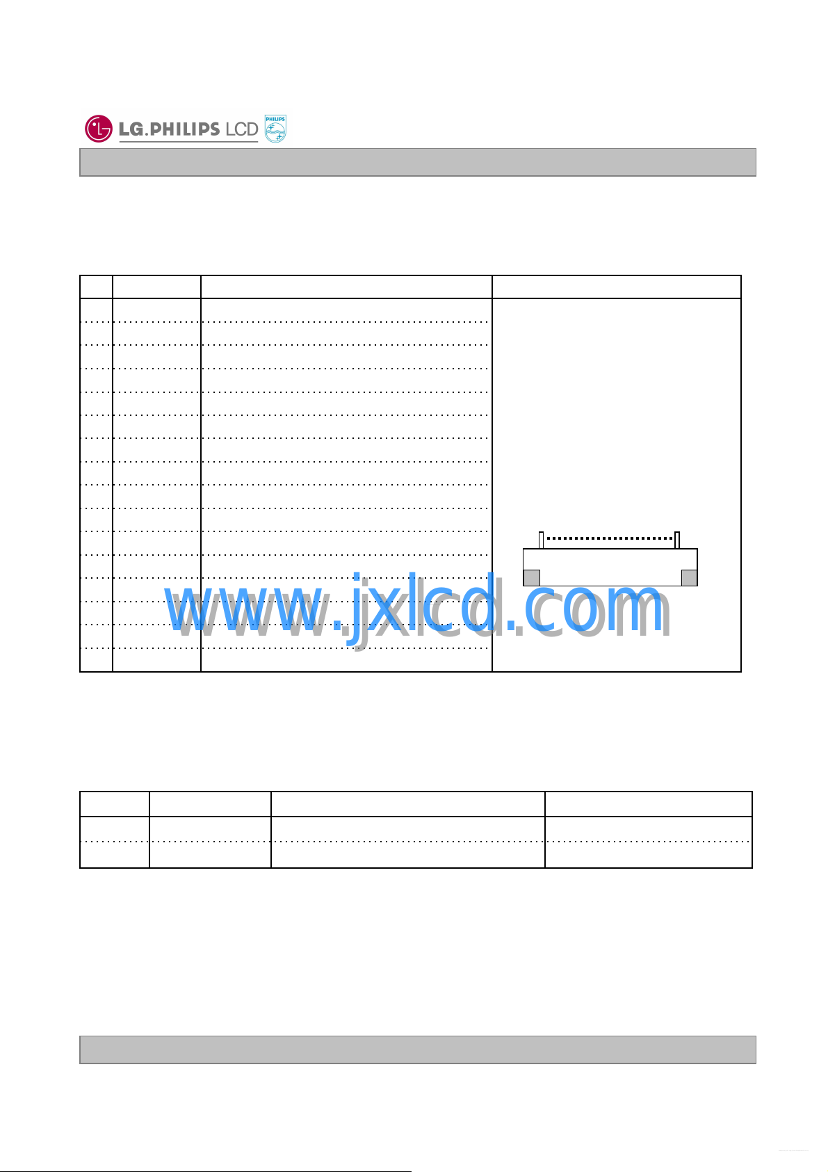
The inverter interface connector(J1) is a
configuration for the connector is shown in the table below.
Table 4. BACKLIGHT INVERTER CONNECTOR PIN CONFIGURATION (J1)
V
IN
2
3
IN
IN
www.jxlcd.com
Power for the inverter 1
Power for the inverter V
Power for the inverter V
GroundGND4
GroundGND5
GroundGND6
Power for the control circuit5V_SUS7
Power for storing a brightness values5V_ALW8
Brightness dataSMB_DAT9
Clock for brightness dataSMB_CLK10
Enable for lamp turn on and offFPVEE11
No connectionNC12
0(GND)PANEL_ID313
0(GND)PANEL_ID214
www.jxlcd.com
1(OPEN)PANEL_ID115
WR-L16S-VF-HD2-1
model manufactured by JAE. The pin
NotesDescriptionSymbolPin
[Connector]
WR-L16S-VF-HD2-1 , JAE
[Connector pin arrangement]
LCD module rear view
16
1
1(OPEN)PANEL_ID020
The backlight interface connector is a model BHSR-02VS-1, manufactured by JST. The mating connector
part number is SM02B-BHSS-1 or equivalent.
Table 5. BACKLIGHT CONNECTOR PIN CONFIGURATION (J3)
NotesDescriptionSymbolPin
1Power supply for lamp (High voltage side)HV1
1Power supply for lamp (Low voltage side)LV2
Notes : 1. The high voltage side terminal is colored pink and the low voltage side terminal is white
Ver. 1.0 DEC. 20, 2002
8 / 29
LP141X8(A1M3)
www.DataSheet.net/
Datasheet pdf - http://www.DataSheet4U.co.kr/
Liquid Crystal Display
Product Specification
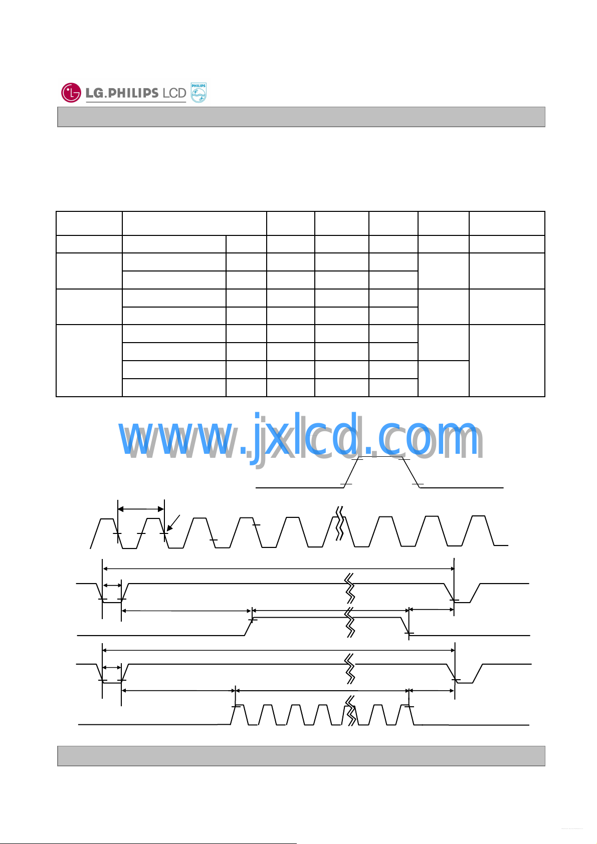
3-3. Signal Timing Specifications
This is the signal timing required at the input of the User connector. All of the interface signal timing should be
satisfied with the following specifications and specifications of LVDS Tx/Rx for it’s proper operation.
Table 6. TIMING TABLE
NoteUnitMaxTypMinSymbolITEM
FrequencyDCLK
PeriodHsync
Width
Vsync
Data
Enable
Period
Width
Horizontal back porch
Horizontal front porch
Vertical back porch
Vertical front porch
3-4. Signal Timing Waveforms
www.jxlcd.com
www.jxlcd.com
Data Enable, Hsync, Vsync
t
DCLK
CLK
0.5 Vcc
CLK
HP
WH
VP
WV
HBP
HFP
VBP
VFP
High: 0.7VCC
Low: 0.3VCC
15.4nsMHz656565f
136413441206t
2401368t
830806780t
24-61t
-16010t
-2410t
-292t
-31t
t
CLK
t
HP
t
CLK
t
HP
Condition : VCC =3.3V
t
Hsync
t
WH
t
HBP
HP
t
WHA
Data Enable
t
VP
t
WV
Vsync
t
VBP
t
WVA
Data Enable
Ver. 1.0 DEC. 20, 2002
t
t
HFP
VFP
9 / 29
 Loading...