

LG LP-141X8-A1 Service manual
LP141X
www.DataSheet.net/
Datasheet pdf - http://www.DataSheet4U.co.kr/
LP141X8888----AAAA1111
Product Specification
Product Specification
Product SpecificationProduct Specification
LP141X LP141X
Liquid Crystal Display
Liquid Crystal Display
Liquid Crystal Display Liquid Crystal Display
SPECIFICATION
FOR
APPROVAL
( ♦♦♦♦ ) Preliminary Specification
( ) Final Specification
Title 14.1” XGA TFT LCD
BUYER Dell(Compal) SUPPLIER LG.Philips LCD Co., Ltd.
MODEL Connery
SUFFIX A1
please use the above model name without suffix.
Please return 1 copy for your confirmation
with your signature and comments.
www.jxlcd.com
www.jxlcd.com
SIGNATURE
/
/
/
DATE
****MODEL
* When you obtain standard approval ,
APPROVED BY
S.H.Kang / S. Manager
REVIEWED BY
S.C.Yoon / Manager
B.H.Koo / Manager
PREPARED BY
M.J.Lee / Engineer
M.K.Jang / Engineer
Product Engineering Dept.
LG.Philips LCD Co., Ltd.
LP141X8
DATE
The preliminary document is subject to change without prior notice.
Ver 0.
Ver 0.2222
Ver 0.Ver 0.
NOV
NOV 3333,
NOVNOV
, 2000
2000 Page
Page 1111/2
, ,
20002000
Page Page
/26666
/2/2

LP141X
www.DataSheet.net/
Datasheet pdf - http://www.DataSheet4U.co.kr/
LP141X8888----AAAA1111
Product Specification
Product Specification
Product SpecificationProduct Specification
LP141X LP141X
Liquid Crystal Display
Liquid Crystal Display
Liquid Crystal Display Liquid Crystal Display
CONTENTS
NO.
- COVER 1
- CONTENTS 2
- RECORD OF REVISIONS 3
1 GENERAL DESCRIPTION 4
2 ABSOLUTE MAXIMUM RATINGS 5
3 ELECTRICAL SPECIFICATIONS 6
3-1 ELECTRICAL CHARACTERISTICS 6
3-2 INTERFACE CONNECTIONS 7
3-3 SIGNAL TIMING SPECIFICATIONS 9
3-4 SIGNAL TIMING WAVEFORMS 10
3-5 COLOR INPUT DATA REFERENCE 11
3-6 POWER SEQUENCE 12
4 OPTICAL SPECIFICATIONS 13
5 MECHANICAL CHARACTERISTICS 16
6 RELIABILITY 20
7 INTERNATIONAL STANDARDS 21
7-1 SAFETY 21
www.jxlcd.com
www.jxlcd.com
ITEM Page
7-2 EMC 21
8 PACKING 22
8-1 DESIGNATION OF LOT MARK 22
8-2 PACKING FORM 22
9 PRECAUTIONS 23
9.1 MOUNTING PRECAUTIONS 23
9.2 OPERATING PRECAUTIONS 23
9.3 ELECTROSTATIC DISCHARGE CONTROL 24
9.4 PRECAUTIONS FOR STRONG LIGHT EXPOSURE 24
9.5 STORAGE 24
9.6 HANDLING PRECAUTIONS FOR PROTECTION FILM 24
A APPENDIX. Enhanced Extended Display Identification Data 25
Ver 0.
Ver 0.2222
Ver 0.Ver 0.
NOV
NOV 3333,
NOVNOV
, 2000
2000 Page
Page 2222/2
, ,
20002000
Page Page
/26666
/2/2
LP141X
www.DataSheet.net/
Datasheet pdf - http://www.DataSheet4U.co.kr/
LP141X8888----AAAA1111
Product Specification
Product Specification
Product SpecificationProduct Specification
LP141X LP141X
Liquid Crystal Display
Liquid Crystal Display
Liquid Crystal Display Liquid Crystal Display
RECORDS OF REVISIONS
Version No Date Page
0.0
0.1
0.2
AUG 30, 2000
SEP 19, 2000
NOV 03, 2000
www.jxlcd.com
www.jxlcd.com
-
4,18
6
13,14
17
4,16
6
9
10
12
13
14
18
DESCRIPTION
First Draft
Change the weight, for the application of VERTICAL
ASSEMBLY (Added INVERTER)
Change 3-1. Electrical Characteristics
Added and changed Table 2 (Parameter)
* Backlight, Inverter parts
Add 3-7. Enhanced Extended Display Identification
Data (EEDID)
Change the gray scale specification.
Change the outline dimensions(Depth)
Change 3-1. Electrical Characteristics
Change 3-3. Signal Timingl specifications(Table 6)
Change 3-4. Signal Timingl Waveforms
Change 3-6. Power Sequence (Add PWR_SRC)
Change 4. Optical specifications(Table 8)
Change the gray scale specification.
Add Note) 2.
25, 26
Change APPENDIX[A] Enhanced Extended Display
Identification Data (EEDID)
Ver 0.
Ver 0.2222
Ver 0.Ver 0.
NOV
NOV 3333,
NOVNOV
, 2000
2000 Page
Page 3333/2
, ,
20002000
Page Page
/26666
/2/2
LP141X
www.DataSheet.net/
Datasheet pdf - http://www.DataSheet4U.co.kr/
LP141X8888----AAAA1111
Product Specification
Product Specification
Product SpecificationProduct Specification
LP141X LP141X
Liquid Crystal Display
Liquid Crystal Display
Liquid Crystal Display Liquid Crystal Display
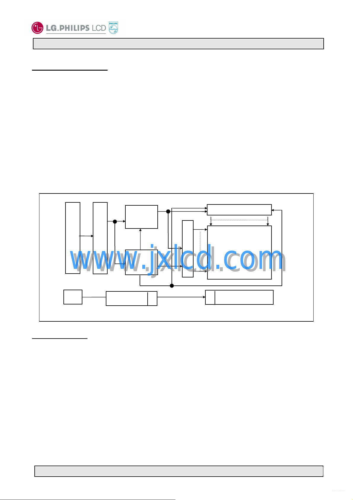
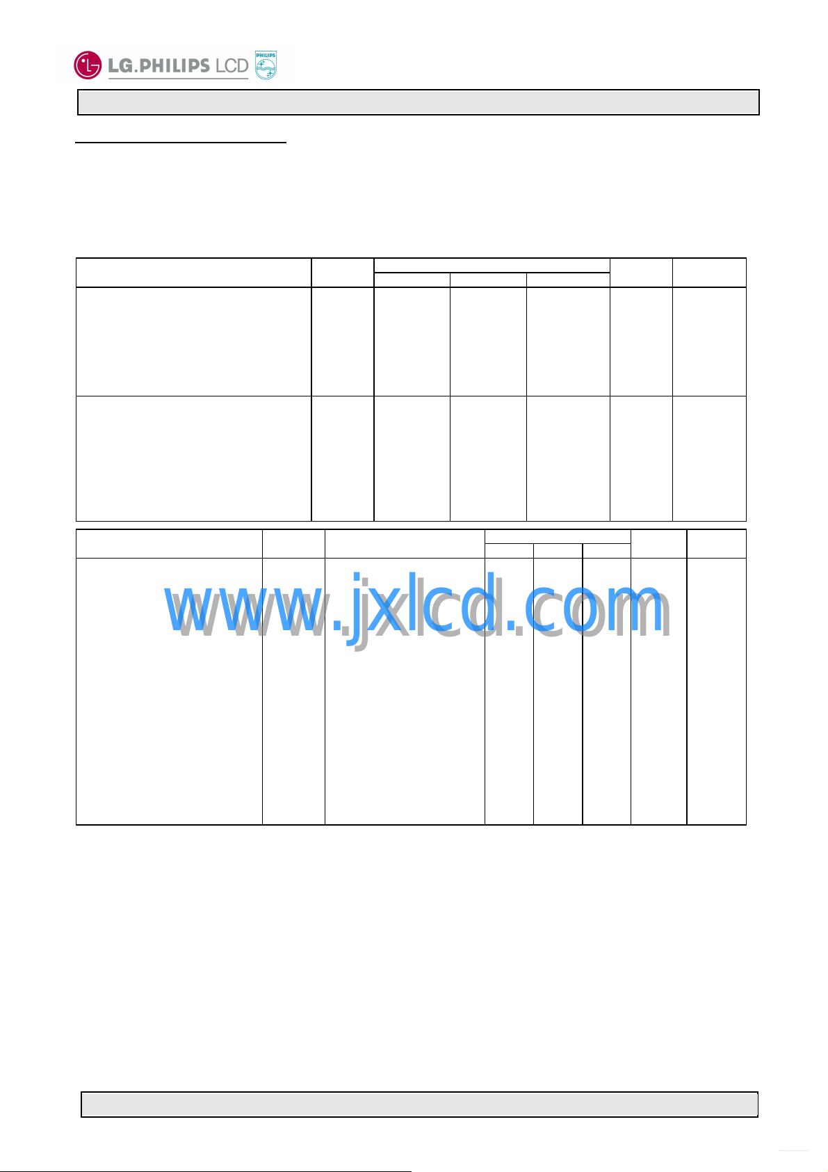
1. General Description
The LP141X8-A1 is a Color Active Matrix Liquid Crystal Display with an integral Cold Cathode Fluorescent
Lamp(CCFL) backlight system. The matrix employs a-Si Thin Film Transistor as the active element. It is a
transmissive type display operating in the normally white mode. This TFT-LCD has a 14.1 inches diagonally
measured active display area with XGA resolution(768 vertical by 1024 horizontal pixel array). Each pixel is
divided into Red, Green and Blue sub-pixels or dots which are arranged in vertical stripes. Gray scale or the
brightness of the sub-pixel color is determined with a 6-bit gray scale signal for each dot, thus, presenting a
palette of more than 262,144 colors.
The LP141X8-A1 has been designed to apply the interface method that enables low power, high speed, low
EMI. Flat Link must be used as a LVDS(Low Voltage Differential Signaling) chip.
The LP141X8-A1 is intended to support applications where thin thickness, low power are critical factors and
graphic displays are important. In combination with the vertical arrangement of the sub-pixels, the LP141X8-A1
characteristics provide an excellent flat panel display for office automation products such as Notebook PC.
Timing
Control
Block
CN1
FlatLink interface
www.jxlcd.com
www.jxlcd.com
J1
B/L Inverter J2
Power
Block
Row Driver circuit
Column driver circuit
TFT-LCD
(1024×768)
J3 Backlight Ass’y
General Features
Active screen size 14.1 inches(35.814cm) diagonal
Outline dimensions 299(H) × 227(V) × 5.7(D) mm (Typ.)
Pixel pitch 0.279 mm × 0.279 mm
Pixel format 1024 horiz. by 768 vert. pixels
RGB stripe arrangement
Color depth 6-bit, 262,144 colors
Luminance,White 150 cd/m2 (Typ.)
Power Consumption Total 6.02Watt(Typ.)
LCM Circuit 1.12Watt(Typ.), Backlight Inverter Input 4.90Watt(Typ.)
Weight 509g (Typ.), 521g (Max.) with the inverter and bracket.
Display operating mode Transmissive mode, normally white
Surface treatments Hard coating (3H),
Anti-glare treatment of the front polarizer
Ver 0.
Ver 0.2222
Ver 0.Ver 0.
NOV
NOV 3333,
NOVNOV
, 2000
2000 Page
Page 4444/2
, ,
20002000
Page Page
/26666
/2/2
LP141X
40
50
60
70 80 0
20
30
50
60
www.DataSheet.net/
Datasheet pdf - http://www.DataSheet4U.co.kr/
LP141X8888----AAAA1111
Product Specification
Product Specification
Product SpecificationProduct Specification
LP141X LP141X
Liquid Crystal Display
Liquid Crystal Display
Liquid Crystal Display Liquid Crystal Display
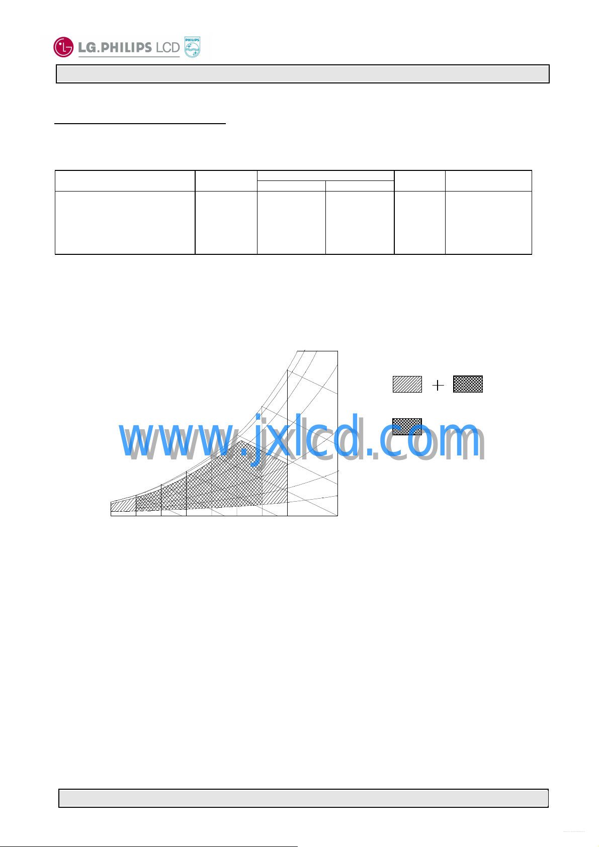
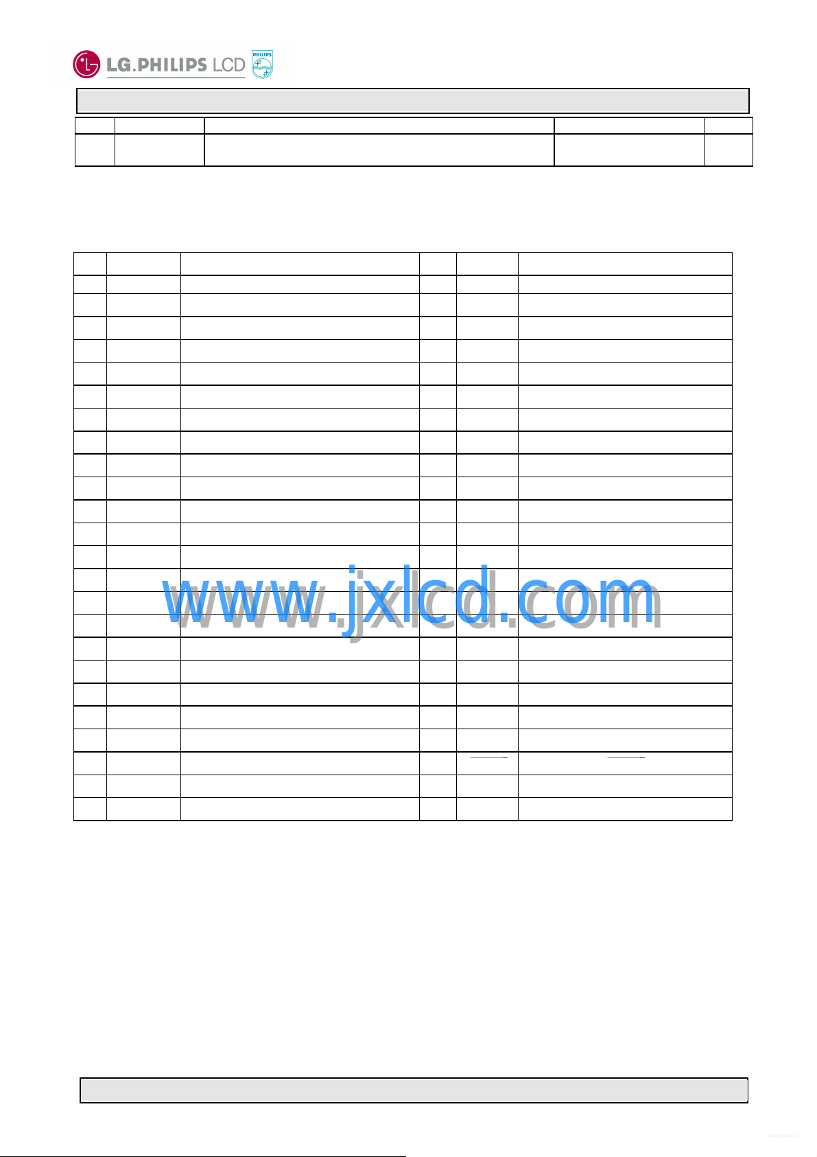
2. Absolute Maximum Ratings
The following are maximum values which, if exceeded, may cause faulty operation or damage to the unit.
Table 1 ABSOLUTE MAXIMUM RATINGS
Parameter symbol
Power Input Voltage
Operating Temperature
Storage Temperature
Operating Ambient Humidity
Storage Humidity
Note: 1. Temperature and relative humidity range are shown in the figure below.
Wet bulb temperature should be 39℃ Max, and no condensation of water.
V
CC
T
OP
T
ST
H
OP
H
ST
Values
Min. Max.
-0.3
0
-20
10
10
4.0
50
60
90
90
Units Notes
Vdc
℃
℃
%RH
%RH
at 25 ±5℃
1
1
1
1
Wet Bulb
Temperature [℃]
www.jxlcd.com
www.jxlcd.com
10
0
-20
10
20 30
Dry Bulb Temperature [℃]
40
95% 80%
60
40
20
10
%
%
%
%
Storage
Operation
Humidity [(%)RH]
Ver 0.
Ver 0.2222
Ver 0.Ver 0.
NOV
NOV 3333,
NOVNOV
, 2000
2000 Page
Page 5555/2
, ,
20002000
Page Page
/26666
/2/2
LP141X
www.DataSheet.net/
Datasheet pdf - http://www.DataSheet4U.co.kr/
LP141X8888----AAAA1111
Product Specification
Product Specification
Product SpecificationProduct Specification
LP141X LP141X
Liquid Crystal Display
Liquid Crystal Display
Liquid Crystal Display Liquid Crystal Display
3. Electrical Specifications
3-1. Electrical Characteristics
The LP141X8-A1 requires two power inputs. One is employed to power the LCD electronics and to drive the
TFT array and liquid crystal. The second input is powers of the Inverter.
Table 2 ELECTRICAL CHARACTERISTICS: (Ta= 25±±±±2℃℃℃℃)
Parameter Symbol
MODULE
Power Supply Input Voltage
Power Supply Input Current
Differential Impedance
Power Consumption
Rush Current
Duration of rush current
BACKLIGHT
Operating Voltage
Operating Current
Operating Frequency
Discharge Stabilization Time
Life Time
Parameter Symbol
Min. Typ. Max.
V
I
RUSH
T
CC
I
CC
Z
m
Pc
RUSH
V
L
IL
F
L
TS
3.0
-
90
-
-
-
680(6mA)
2.7
45
-
10,000
Condition
Values
3.3
0.340
100
1.12
1.0
-
725(5mA)
910(2.7mA)
5.0
58
-
-
Min. Typ. Max.
3.6
0.375
110
1.24
1.5
30
6.0
80
3
-
Values
Units Notes
Vdc
A
Ohm
W
A
ms
V
rms
mA
rms
kHz
min
Hours
1
2
1
3
4
IL =6.0mA
Units Notes
INVERTER (Ambit/Sumida)
Input Voltage
Input Current
Input Power Consumption
Backlight On/Off Control
www.jxlcd.com
www.jxlcd.com
Backlight Adjust
(Lamp Current Control)
Output Voltage
Output Curren
Operating Frequency
Output Power Consumption
Open Lamp Voltage
Efficiency
Striking Time
INV-SRC
Iin
P
in
FPVEE
SMB-DAT
V
out
Iout
Freq.
P
out
V
open
η
Ts
(=Vin, PWR_SRC)
Vin=14.4V, Iout=5.8mA
Vin=14.4V, Iout=5.8mA
FRVEE=High
FRVEE=Low
* 00H=Luminance max.
Vin=14.4V, Iout=5.8mA
Ta=25℃,Aging 20minutes
SMB-DAT=FFH (min.)
SMB-DAT=00H (max.)
Vin=14.4V, Iout=5.8mA
Vin=14.4V, Iout=5.8mA
No Load, Vin=9V
Vin=9V, Iout=5.8mA
9.0
290
4.17
2.0
-0.3
FFH
580
2.7
5.5
50
3.36
1450
80
0.6
14.4
340
4.90
-
-
680
3.0
5.8
60
3.94
-
-
1.0
21.0
390
5.62
5.25
0.8
00H
780
3.3
6.0
70
4.52
-
-
1.4
Vdc
mA
W
Vdc
Vdc
Vrms
mA
rms
mA
rms
KHz
W
Vrms
%
sec
Notes: 1. The specified current and power consumption are under the Vcc = 3.3V , 25℃, fv = 60Hz condition
whereas full black pattern is displayed and fv is the frame frequency.
2. This impedance value is needed to proper display and measured from LVDS Tx to the mating
connector.
3. Define the brightness of the lamp after being lighted for 5 minutes as 100, TS is the time required for
the
brightness of the center of the lamp to be not less than 95%.
4. The life time is determined as the time at which brightness of lamp is 50% compared to that of initial
value at the typical lamp current on condition of continuous operating at 25 ±2℃.
5. The specified total power consumption is the sum of the module and inverter input under the
Vcc = 3.3V , fv = 60Hz, Dclk=65MHz, 25℃, Vin=14.4V, Iout=5.8mA, SMB-DAT=00H
Ver 0.
Ver 0.2222
Ver 0.Ver 0.
NOV
NOV 3333,
NOVNOV
, 2000
2000 Page
Page 6666/2
, ,
20002000
Page Page
/26666
/2/2

LP141X
www.DataSheet.net/
Datasheet pdf - http://www.DataSheet4U.co.kr/
LP141X8888----AAAA1111
Product Specification
Product Specification
Product SpecificationProduct Specification
LP141X LP141X
Liquid Crystal Display
Liquid Crystal Display
Liquid Crystal Display Liquid Crystal Display
3-2. Interface Connections
The interface connections are compatible with ISP (Industry Standard Panels) 14.1” Mounting and Top
Level Interface Requirements (Version2, June,2000) defined by SPWG (Standard Panels Working Group).
This LCD employs two interface connections, a 20 pin connector is used for the module electronics and the
other connector is used for the integral backlight system.
The electronics interface connector is a model GT122-20P-H15-R manufactured by LG Cable. The pin
configuration for the connector is shown in the table below.
Table 3 MODULE CONNECTOR PIN CONFIGURATION (LVDS) [CN1]
Pin
1
2
3
4
5
6
7
8
9
10
11
12
13
14
15
16
17
18
19
20
The backlight interface connector(J3) is a BHSR-02VS-1(JST, 2pin), and the mating connector(J2) is a SM02BBHSS-1(JST) or equivalent. The Inverter interface connector(J1) is a WR-L16S-VF-HD2-1(JAE, 16pin).
The pin configuration for the connector is shown in the table belows.
Inverter interface connector (J1)
Pin
1
2
3
4
5
6
7
8
9
10
11
12
13
14
15
16
Backlight interface connector(J3)
Symbol Description Notes
PWR_SRC
PWR_SRC
PWR_SRC
Backlight_On
PANEL_ID3
PANEL_ID2
PANEL_ID1
PANEL_ID0
Vcc
Vcc
GND
GND
A0M
A0P
GND
A1M
A1P
GND
A2M
A2P
GND
CLKM
CLKP
GND
VEDID
NC
Clk_EDID
Data_EDID
www.jxlcd.com
www.jxlcd.com
Table 4 BACKLIGHT INVERTER CONNECTOR PIN CONFIGURATION(J1, J3)
Symbol Voltage Description Notes
GND
GND
GND
5V_SUS
5V_ALW
SMB_DAT
SMB_CLK
NC
4.85V to 5.2V
4.85V to 5.2V
LCD VDD (3.3V)
LCD VDD (3.3V)
Differential Signal
Differential Signal
Differential Signal
Differential Signal
Differential Signal
Differential Signal
Differential Signal
Differential Signal
No Connection
9.0V to 21V
9.0V to 21V
0V
9.0V to 21V
0V
0V
(= FPVEE)
Ground
Ground
Ground
Ground
Ground
Ground
VEDID
Clk_EDID
Data_EDID
This power rail should be used as a power source for inverter.
This power rail should be used as a power source for inverter.
This power rail should be used as a power source for inverter.
This should be used as a power source for the control circuit on
the inverter.
This should be used as a power source that store the brightness
values and interface with SMB_CLK and SMB_DAT.
SMBus interface for sending brightness information to the inverter.
SMBus interface for sending brightness information to the inverter.
Control signal input into the inverter to turn the backlight ON.
1 (OPEN)
1 (OPEN)
1. Interface chips
1.1 LCD : SN75LVDS88B (TI)
(SN75LVDS84 core + Timing Controller)
1.2 System : SN75LVDS86(TI)
2. Connector (SPWG Style “A” compatible)
2.1 LCD : GT122-20P-H15-R (LG Cable)
2.2 Mating : FI-SE20M-HF(JAE) or compatible
2.3 Connector pin arrangement
< Viewing on Display side >
Ground
Ground
Ground
No Connection
0 (Connected to GND)
0 (Connected to GND)
1 … 20
CN1
J1
Inverter
J2
J3
1
1
1
1
Ver 0.
Ver 0.2222
Ver 0.Ver 0.
NOV
NOV 3333,
NOVNOV
, 2000
2000 Page
Page 7777/2
, ,
20002000
Page Page
/26666
/2/2
LP141X
www.DataSheet.net/
Datasheet pdf - http://www.DataSheet4U.co.kr/
LP141X8888----AAAA1111
Product Specification
Product Specification
Product SpecificationProduct Specification
LP141X LP141X
Liquid Crystal Display
Liquid Crystal Display
Liquid Crystal Display Liquid Crystal Display
Pin
1
2
Symbol Description Terminal Color Notes
HV
LV
Power supply for lamp (High voltage side)
Power supply for lamp (Low voltage side)
Notes: 1. The PANEL_ID of LP141X8-A1 is 0011(ID3 to ID0).
Table 5 REQUIRED SIGNAL ASSIGNMENT FOR FlatLink Transmitter
Pin # Pin Name
1 D4 R4 48
2 Vcc Vcc 47
3 D5 R5 46
4 D6 G0 45
5 GND GND 44
6 D7 G1 43
7 D8 G2 42 LVDS GND
8 Vcc Vcc 41
9 D9 G3 40
10
11
12
13
14
15
16
17
18
19
20
21
22
23
24
D10 G4 39
GND GND 38
D11 G5 37 LVDS Vcc
D12 B0 36 LVDS GND
NC NC 35
D13 B1 34
www.jxlcd.com
www.jxlcd.com
D14 B2 33 CLKOUTM
GND GND 32 CLKOUTP
D15 B3 31 LVDS GND
D16 B4 30 PLLGND
D17 B5 29 PLLVcc
Vcc Vcc 28 PLLGND
D18 HSYNC 27
D19 VSYNC 26 CLKIN Dclk
GND GND 25
Require Signals Pin # Pin Name
GND GND
Y0M A0M
Y0P A0P
Y1M A1M
Y1P A1P
Y2M A2M
Y2P A2P
SHDN SHDN
D20 DE(Data Enable)
Pink
White
Require Signals
D3 R3
D2 R2
D1 R1
D0 R0
NC NC
LVDS GND
LVDS Vcc
LVDS GND
CLKM
CLKP
LVDS GND
PLL GND
PLL Vcc
PLL GND
Notes : Refer to LVDS Transmitter Data Sheet for detail descriptions.
Ver 0.
Ver 0.2222
Ver 0.Ver 0.
NOV
NOV 3333,
NOVNOV
, 2000
2000 Page
Page 8888/2
, ,
20002000
Page Page
/26666
/2/2
 Loading...