

LG LP-141X6-A11B Service manual
www.DataSheet4U.com
( DataSheet : www.DataSheet4U.com )
SPECIFICATIONS
LP141X6-A1IB LIQUID CRYSTAL DISPLAY
DATA DISPLAY AG
TITLE: LP141X6-A1IB REV. 1 PAGE 1 OF 22
LP141X6-A1IB
14.1“ XGA TFT LCD
www.jxlcd.com
www.jxlcd.com
PRELIMINARY
SPECIFICATION
The information given in this document is carefully checked and believed to be reliable. Data Display reserves the
right to make changes in product or specification at any time and without further notice. Data Display products are
not intended for use in systems in which failures of product could result in personal injury. All mentioned trademarks
are registered trademarks of their owner. LG.Philips LCD: Rev. 0.2 Oct.6, 1999
DATA DISPLAY AG
Industriestrasse 1
D-82110 Germering
OCT 2000
http://www.datadisplay.de
Tel.: +49-89-894450-0
Fax: +49-89-894450-90
interface
SPECIFICATIONS
LP141X6-A1IB LIQUID CRYSTAL DISPLAY
1. GENERAL DESCRIPTION
The LP141X6-A1IB is a Color Active Matrix Liquid Crystal Display with an integral
Cold Cathode Fluorescent Lamp(CCFL) back light system. The matrix employs a-Si
Thin Film Transistor as the active element. It is a transmissive type display operating
in the normally white mode. This TFT-LCD has a 14.1 inch diagonally measured
active display area with XGA resolution(768 vertical by 1024 horizontal pixel array).
Each pixel is divided into Red, Green and Blue sub-pixels or dots which are
arranged in vertical stripes. Gray scale or the brightness of the sub-pixel color is
determined with a 6-bit gray scale signal for each dot, thus, presenting a palette of
more than 262,144 colors. The LP141X6-A1IB has been designed to apply the
interface method that enables low power, high speed low EMI. Flat Link must be
used as a LVDS(Low Voltage Differential Signaling) chip. The LP141X6-A1IB is
intended to support applications where thin thickness, low power are critical factors
and graphic displays are important. In combination with the vertical arrangement of
the sub-pixels, the LP141X6-A1IB characteristics provide an excellent flat panel
display for office automation products such as mobile industrial computers.
TITLE: LP141X6-A1IB REV. 1 PAGE 2 OF 22
www.jxlcd.com
www.jxlcd.com
General Features
Active screen size 14.1 inches (33.78 cm) diagonal
Outline dimensions 298.5 (H) × 227.5 (V) × 5.7 (D) mm (typ)
Pixel pitch 0.279 mm × 0.279 mm
Pixel format 1024 horiz. By 768 vert. Pixel RGB stripe arrangement
Color depth 6-bit, 262,144 colors
Luminance, White 150 cd/m
Power Consumption Total 4.54 Watt (typ)
Weight 500g (typ)
Display operating mode transmissive mode, normally white
Surface treatments hard coating(3H),
anti-glare treatment of the front polarizer
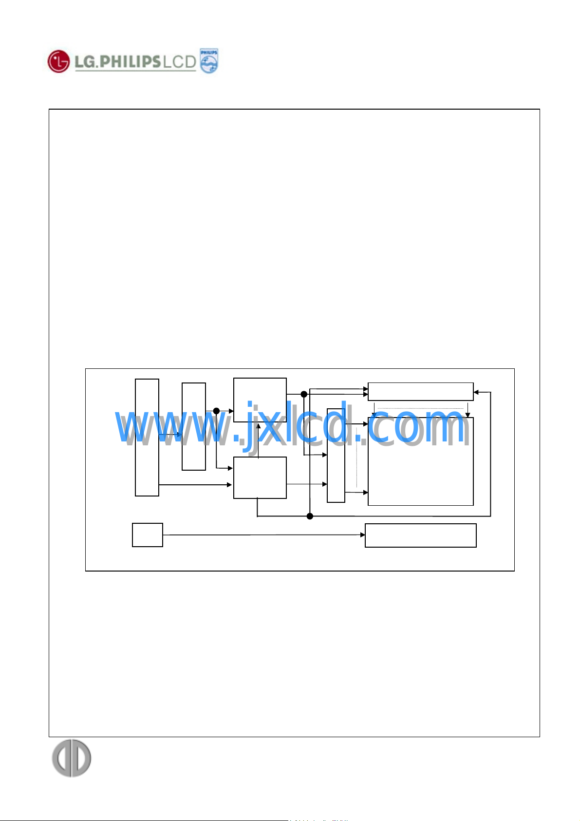
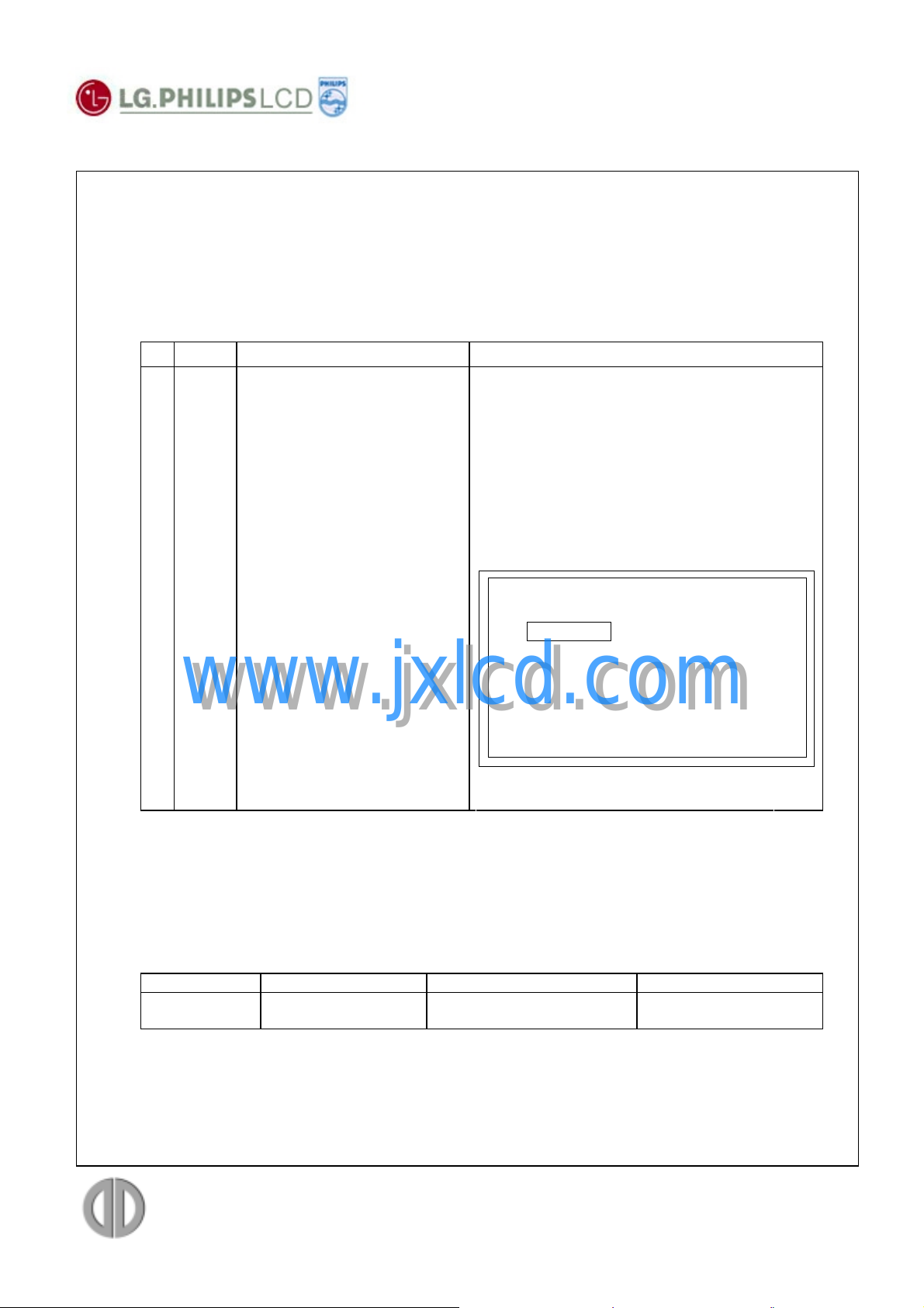
CN1
CN2
FlatLink
Timing
Control
Block
Power
Block
2
(typ)
Column driver circuit
TFT-LCD
(1024××××768)
Row Driver circuit
Backlight Ass’y
DATA DISPLAY AG
Industriestrasse 1
D-82110 Germering
OCT 2000
http://www.datadisplay.de
Tel.: +49-89-894450-0
Fax: +49-89-894450-90
SPECIFICATIONS
LP141X6-A1IB LIQUID CRYSTAL DISPLAY
2. ABSOLUTE MAXIMUM RATINGS
The following are maximum values which, if exceeded, may cause faulty operation
or damage to the unit.
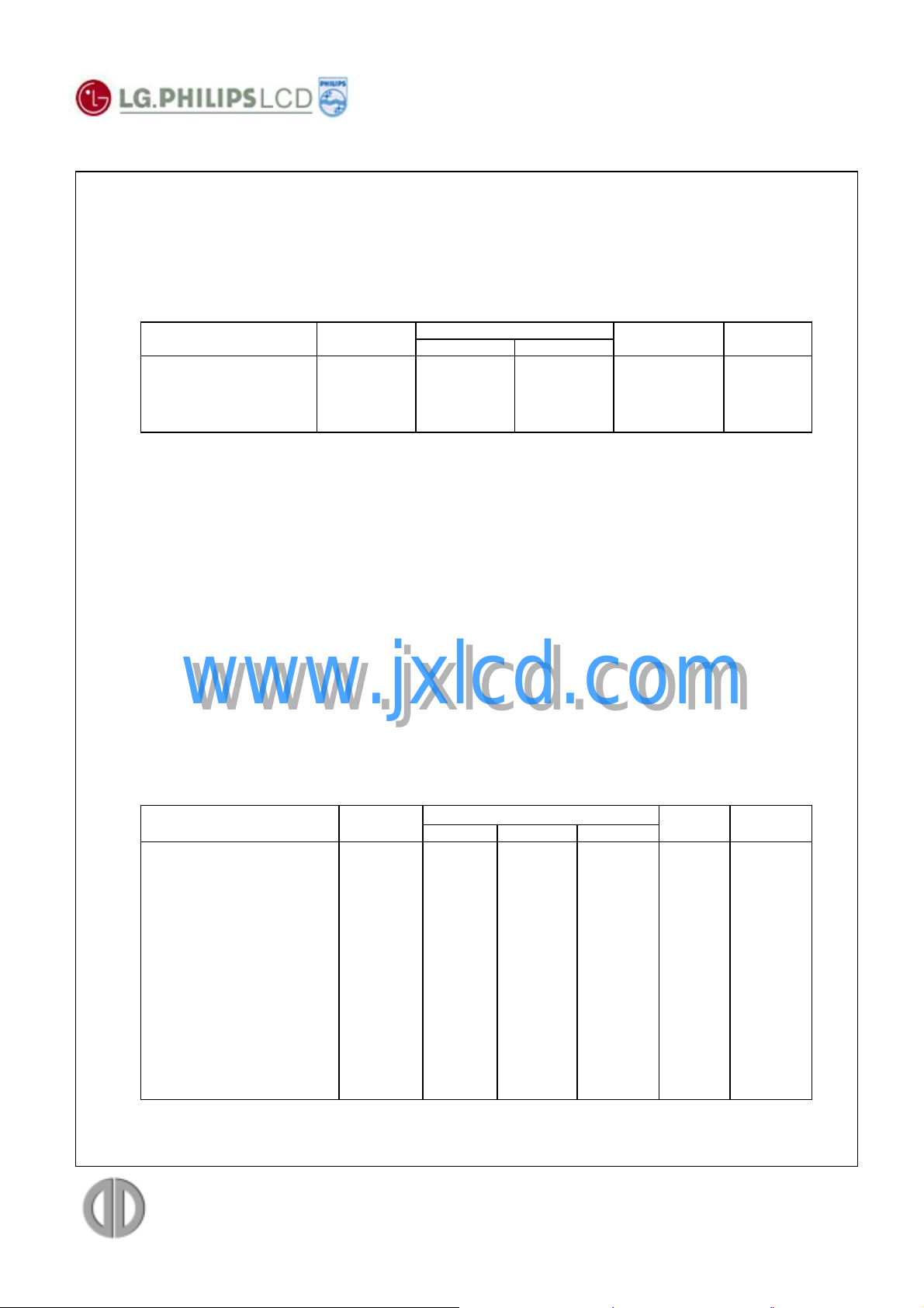
Table 1 ABSOLUTE MAXIMUM RATINGS
Parameter Symbol
Power Input Voltage
Operating Temperature
Storage Temperature
V
CC
TOP
T
ST
Note 1: Temperature at 5 mm above display center of LCD Module.
Ta ≤ 40°C: 90 % RH max
Ta > 40°C: Absolute Humidity shall be less than Ta = 40° 90 % RH.
These shall be no dew condensation.
Note 2: Humidity Min. 5% RH, Max. 90% RH
3. ELECTRICAL SPECIFICATIONS
TITLE: LP141X6-A1IB REV. 1 PAGE 3 OF 22
Values
Min. Max.
-0.3
0
-20
+3.6
+50
+60
Units Notes
Vdc
°C
°C
at 25°
1,2
1,2
3.1 Electrical Characteristics
The LP141X6-A1IB requires two power inputs. One is employed to power the LCD
www.jxlcd.com
electronics and to drive the TFT array and liquid crystal. The second input which
www.jxlcd.com
powers the CCFL, is typically generated by an inverter. The inverter is an external
unit to the LCD.
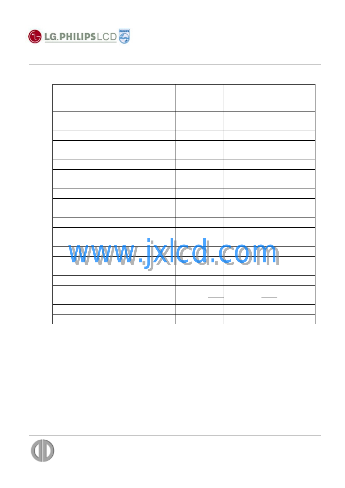
Table 2 ELECTRICAL CHARACTERISTICS
Parameter Symbol
Min. Typ. Max.
MODULE:
Power Supply Input Voltage
Power Supply Input Current
Differential Impedance
Power Consumption
Rush current
LAMP
Operating Voltage
Operating Current
Established Starting
Voltage
at 25°C
at 0°C
Operating Frequency
Power Consumption
Half Life Time
V
I
CC
Zm
P
I
RUSH
V
IBL
f
PBL
CC
BL
c
BL
3.0
-
90
-
-
680
3.0
-
-
40
-
10,000
Values
3.3
0.275
100
0.91
1.0
725
5.0
-
-
60
3.63
15,000
3.6
0.315
110
1.04
1.5
850
6.0
1170
1450
80
4.08
-
Units Notes
Vdc
A
ohm
Watts
A
V
RMS
mA
V
RMS
V
RMS
kHz
Watts
Hrs
1
2
1
3
4
5
6
7
Notes 1: The specified current and power consumption are under the Vcc = 3.3V,
25°C, fv = 60 Hz condition whereas Black pattern is displayed.
DATA DISPLAY AG
Industriestrasse 1
D-82110 Germering
OCT 2000
http://www.datadisplay.de
Tel.: +49-89-894450-0
Fax: +49-89-894450-90
SPECIFICATIONS
LP141X6-A1IB LIQUID CRYSTAL DISPLAY
Notes 2: This impedance value is needed to proper display and measured form
LVDS Tx to the mating connector.
Notes 3: The duration of rush current is about 20 ms.
Notes 4: The variance of the voltage is ± 10 %.
Notes 5: The transformer output voltage in the inverter must be high considering to
the loss of the ballast capacitor in the inverter.
Notes 6: The lamp power consumption shown above does not include loss of
external inverter.
Notes 7: The life time is determined as the time at which brightness of lamp is 50 %
compare to that of initial value at the typical lamp current
TITLE: LP141X6-A1IB REV. 1 PAGE 4 OF 22
www.jxlcd.com
www.jxlcd.com
DATA DISPLAY AG
Industriestrasse 1
D-82110 Germering
OCT 2000
http://www.datadisplay.de
Tel.: +49-89-894450-0
Fax: +49-89-894450-90
SPECIFICATIONS
LP141X6-A1IB LIQUID CRYSTAL DISPLAY
3.2 Interface Connections
This LCD employs two interface connections, a 20 pin connector is used for the
module electronics and the other connector is used for the integral backlight system.
The electronics interface connector is a model FI-SEB-20P-HF manufactured by JAE
or equivalent. The pin configuration for the connector is shown in the table below.
Table 3 MODULE CONNECTOR PIN CONFIGURATION (LVDS) [CN1]
Pin Symbol Description Notes
1
2
3
4
5
6
7
8
9
10
11
12
13
14
15
16
17
18
19
20
VCC
VCC
GND
GND
A0M
A0P
GND
A1M
A1P
GND
A2M
A2P
GND
CLKM
CLKP
GND
NC
NC
GND
www.jxlcd.com
GND
www.jxlcd.com
Power (3.3V)
Power (3.3V)
Ground
Ground
Difference Signal
Difference Signal
Ground
Difference Signal
Difference Signal
Ground
Difference Signal
Difference Signal
Ground
Difference Signal
Difference Signal
Ground
No Connection
No Connection
Ground
Ground
The backlight interface connector is a model BHSR-02VS-1, manufactured by JST.
The mating connector part number is SM02B-BHSS-1 or equivalent. The pin
configuration for the connector is shown in the table below.
Table 4 BACKLIGHT CONNECTOR PIN CONFIGURATION [CN2]
Pin Symbol Description Notes
1
2
Notes 1: The high voltage input terminal is colored white.
Notes 2: The low voltage input terminal is colored black.
HV
LV
TITLE: LP141X6-A1IB REV. 1 PAGE 5 OF 22
1. Interface chips
1.1 LCD: KZ4E038C12CFP (Thine)
(THC63LVDF64A core + Timing Controller)
1.2 System: THC63LVDM63A (Thine)
* Pin to pin compatible with TI LVDS
2. Connector
2.1 LCD: GT122-20P-R (LG CABLE)
2.2 Mating: FI-WEB21P-HF (JAE)
2.3 Connector pin arrangement
No. 1-20
CN1
Viewing on Display side
High voltage input
Low voltage input
1
2
CN2
DATA DISPLAY AG
Industriestrasse 1
D-82110 Germering
OCT 2000
http://www.datadisplay.de
Tel.: +49-89-894450-0
Fax: +49-89-894450-90
SPECIFICATIONS
LP141X6-A1IB LIQUID CRYSTAL DISPLAY
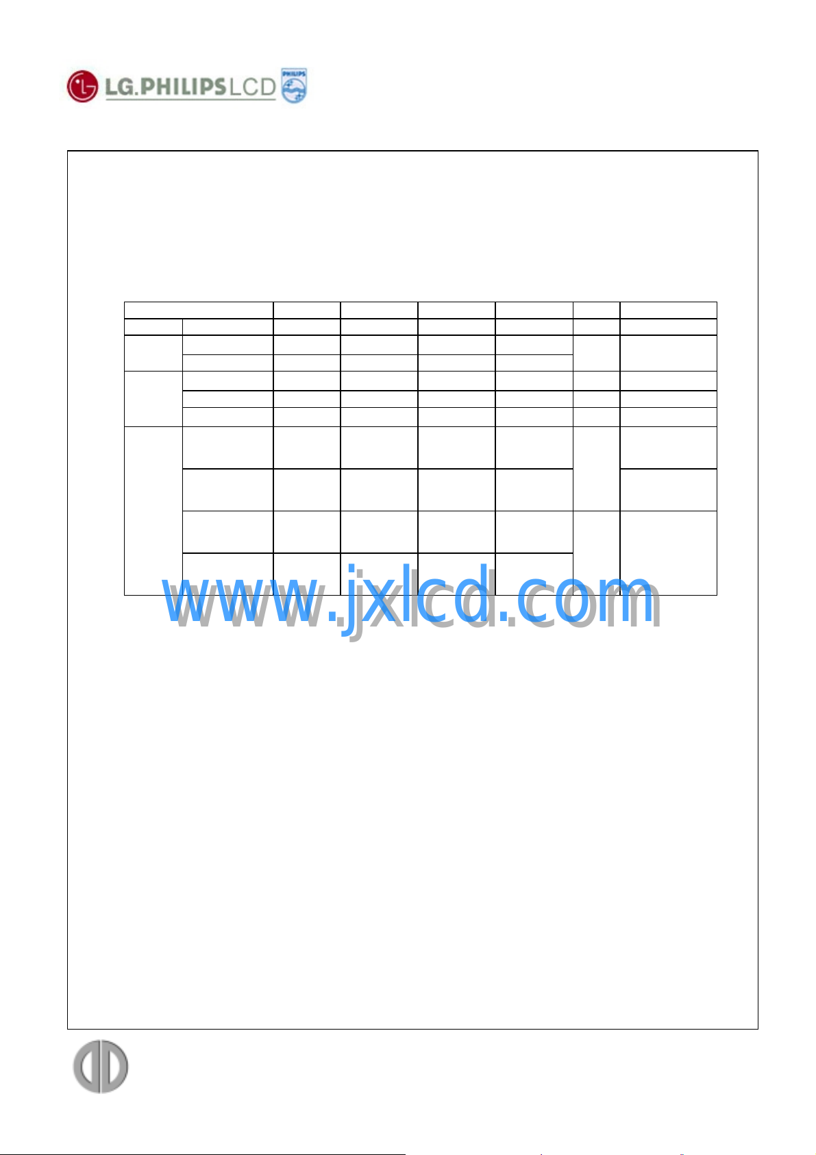
Table 5 REQUIRED SIGNAL ASSIGNMENT FOR FLATLINK TRANSMITTER
Pin # Pin Name Require Signals Pin # Pin Name Require Signals
1 D4 R4 48 D3 R3
2 Vcc Vcc 47 D2 R2
3 D5 R5 46 GND GND
4 D6 G0 45 D1 R1
5 GND GND 44 D0 R0
6 D7 G1 43 NC NC
7 D8 G2 42 LVDS GND LVDS GND
8 Vcc Vcc 41 Y0M A0M
9 D9 G3 40 Y0P A0P
10 D10 G4 39 Y1M A1M
11 GND GND 38 Y1P A1P
12 D11 G5 37 LVDS Vcc LVDS Vcc
13 D12 B0 36 LVDS GND LVDS GND
14 NC NC 35 Y2M A2M
15 D13 B1 34 Y2P A2P
16 D14 B2 33 CLKOUTM CLKM
17 GND GND 32 CLKOUTP CLKP
www.jxlcd.com
18 D15 B3 31 LVDS GND LVDS GND
www.jxlcd.com
19 D16 B4 30 PLLGND PLL GND
20 D17 B5 29 PLLVcc PLL Vcc
21 Vcc Vcc 28 PLLGND PLL GND
22
23 D19 VSYNC 26 CLKIN Dclk
24 GND GND 25 D20 DE (Data Enable)
Notes: Refer to LVDS Transmitter Data Sheet for detail descriptions.
D18 HSYNC 27 SHDN SHDN
TITLE: LP141X6-A1IB REV. 1 PAGE 6 OF 22
DATA DISPLAY AG
Industriestrasse 1
D-82110 Germering
OCT 2000
http://www.datadisplay.de
Tel.: +49-89-894450-0
Fax: +49-89-894450-90
SPECIFICATIONS
LP141X6-A1IB LIQUID CRYSTAL DISPLAY
3.3 Signal Timing Specificat ions
This is the signal timing required at the input of the LVDS Transmitter. All of the
interface signal timing should be satisfied with the following specifications for it’s
proper operation.
Table 6 Timing Table
ITEM SYMBOL MIN. TYP. MAX. UNIT NOTE
Dclk Period t
Hsync Period tHP 1206 1344 1364
Width-Active tWH 16 136 240
Vsync Period tVP 780 806 830
Frequency fV - 60 - Hz
Width-Active tWV 1 6 24
DE
( Data
Enable )
Horizontal
Back Porch
Horizontal
Front Porch
Vertical
Back Porch
Vertical
Front Porch
t
t
t
t
CLK
HBP
HFP
VBP
VFP
TITLE: LP141X6-A1IB REV. 1 PAGE 7 OF 22
14.7 15.4 16.1 ns 65MHz(Typ)
10 160 -
10 24 -
2 29 -
1 3 -
t
CLK
t
HP
t
HP
t
CLK
t
HP
www.jxlcd.com
www.jxlcd.com
DATA DISPLAY AG
Industriestrasse 1
D-82110 Germering
OCT 2000
http://www.datadisplay.de
Tel.: +49-89-894450-0
Fax: +49-89-894450-90
 Loading...