

LP141X13(B1)
www.DataSheet.net/
Datasheet pdf - http://www.DataSheet4U.co.kr/
Liquid Crystal Display
Product Specification
SPECIFICATION
FOR
APPROVAL
)
(
(
Preliminary SpecificationV
)
Final Specification
Title 14.1” XGA TFT LCD
BUYER
MODEL
www.jxlcd.com
www.jxlcd.com
DATESIGNATURE
/
/
/
SUPPLIER LG.Philips LCD Co., Ltd.
*MODEL LP141X13
Suffix B1
*When you obtain standard approval,
please use the above model name without suffix
S.H. Kang / G.Manager
REVIEWED BY
J.H. Park / Manager
/ Manager
PREPARED BY
C.J. Jun / Engineer
/ Engineer
DATESIGNATURE
Please return 1 copy for your confirmation with
your signature and comments.
Ver. 0.0 FEB. 20, 2002
Products Engineering Dept.
LG. Philips LCD Co., Ltd
1/ 29
Product Specification
www.DataSheet.net/
Datasheet pdf - http://www.DataSheet4U.co.kr/
Contents
LP141X13(B1)
Liquid Crystal Display
No ITEM
COVER
CONTENTS
RECORD OF REVISIONS
1 GENERAL DESCRIPTION
2 ABSOLUTE MAXIMUM RATINGS
3 ELECTRICAL SPECIFICATIONS
3-1 ELECTRICAL CHARACTREISTICS
3-2 INTERFACE CONNECTIONS
3-3 SIGNAL TIMING SPECIFICATIONS
3-4 SIGNAL TIMING WAVEFORMS
3-5 COLOR INPUT DATA REFERNECE
www.jxlcd.com
www.jxlcd.com
3-6 POWER SEQUENCE
4 OPTICAL SFECIFICATIONS
5 MECHANICAL CHARACTERISTICS
Page
1
2
3
4
5
6
7
9
9
10
11
12
16
6 RELIABLITY
7 INTERNATIONAL STANDARDS
7-1 SAFETY
7-2 EMC
8 PACKING
8-1 DESIGNATION OF LOT MARK
8-2 PACKING FORM
9 PRECAUTIONS
A APPENDIX. Enhanced Extended Display Identification Data
B APPENDIX. Inspection Criteria
Ver. 0.0 FEB. 20, 2002
20
21
21
22
22
23
25
28
2/ 29
LP141X13(B1)
www.DataSheet.net/
Datasheet pdf - http://www.DataSheet4U.co.kr/
Liquid Crystal Display
Product Specification
RECORD OF REVISIONS
Revision No Revision Date Page Description Note
0.0 FEB.20.2002 - First Draft
www.jxlcd.com
www.jxlcd.com
Ver. 0.0 FEB. 20, 2002
3/ 29
LP141X13(B1)
www.DataSheet.net/
Datasheet pdf - http://www.DataSheet4U.co.kr/
Liquid Crystal Display
Product Specification
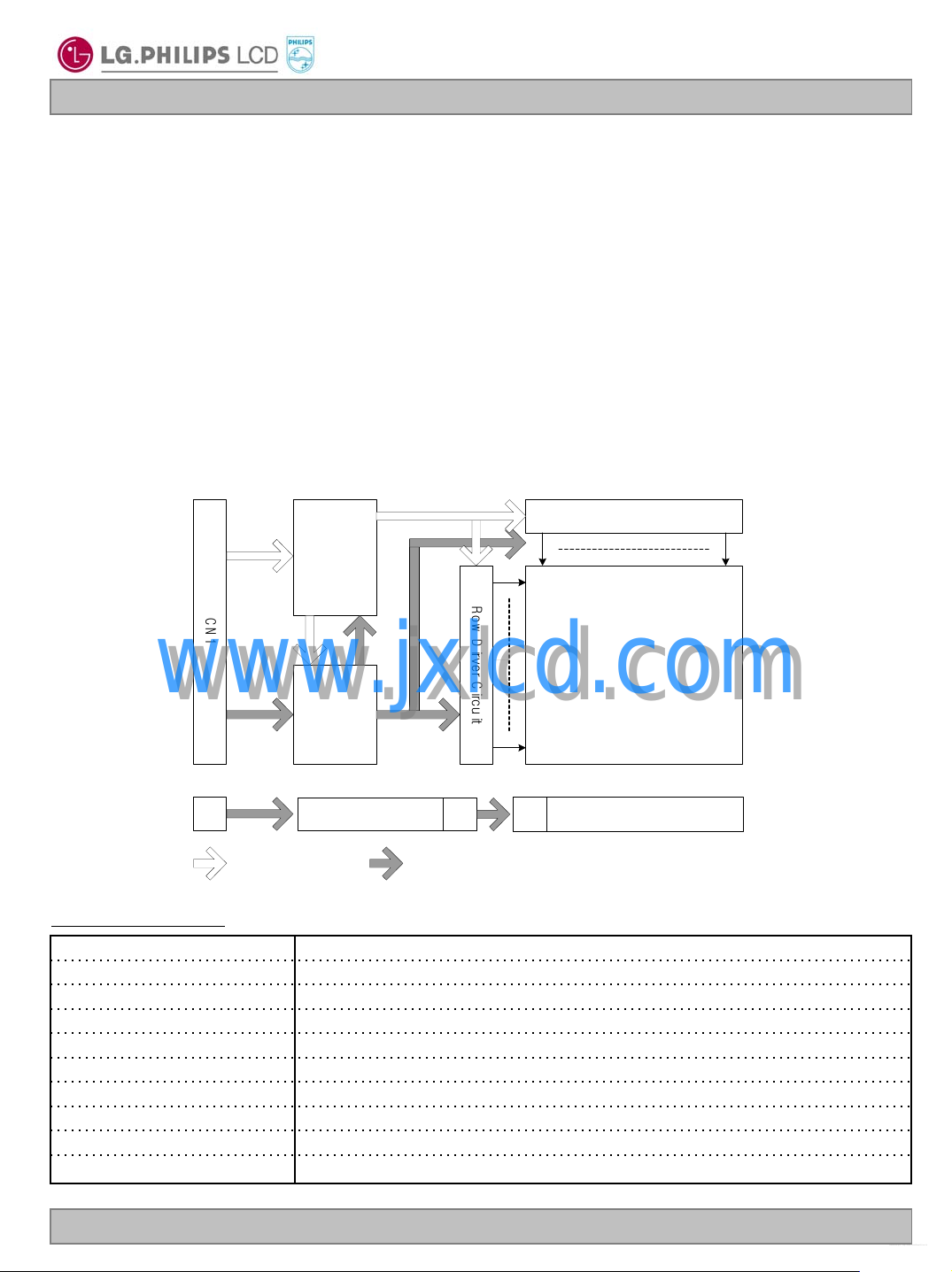
1. General Description
The LP141X13(B1) is a Color Active Matrix Liquid Crystal Display with an integral Cold Cathode
Fluorescent Lamp (CCFL) backlight system. The matrix employs a-Si Thin Film Transistor as the active
element. It is a transmissive type display operating in the normally white mode. This TFT-LCD has 14.1
inches diagonally measured active display area with XGA resolution(768 vertical by 1024 horizonta l pixel
array). Each pixel is divided into Red, Green and Blue sub-pixels or dots which are arranged in vertical
stripes. Gray scale or the brightness of the sub-pixel color is determined with a 6-bit gray scale signal for
each dot, thus, presenting a palette of more than 262,144 colors.
The LP141X13(B1) has been designed to apply the inte rface method that enables low power, high speed,
low EMI.
The LP141X13(B1) is intended to support applications where thin thickness, low power are c ritical factors
and graphic displays are important. In combination with the vertical arrangement of the sub-pixels, the
LP141X13(B1) characteristics provide an excellent flat display for office automation products such as
Notebook PC.
LVD S
&
Timing
Control
Block
C
N
1
www.jxlcd.com
www.jxlcd.com
J1
:C ontrol & D a ta :P o w e r
Power
Block
B/L Inverter
R
o
w
D
i
r
v
e
r
C
i
r
c
u
i
t
J2
Colum n D riv e r C ircuit
TFT-LC D
(1024 X 768)
J3
Backlight A ss'y
General Features
Active Screen Size 14.1 inches(35.814cm) diagonal
Outline Dimension 299(H) × 226.5(V) × 5.5(D) mm (Typ.)
Pixel Pitch 0.279 mm × 0.279 mm
Pixel Format 1024 horiz. By 768 vert. Pixels RGB strip arrangement
Color Depth 6-bit, 262,144 colors
2
Luminance, White 150 cd/m
Power Consumption Total 5.0 Watt(Typ.)
Weight 435 g (Max.) w/o inverter and bracket, 450g(Max.) w/ inverter and bracket
Display Operating Mode Transmissive mode, normally white
Surface Treatment Hard coating(3H) Anti-glare treatment of the front polarizer
(Min.), 5p average
Ver. 0.0 FEB. 20, 2002
4/ 29
LP141X13(B1)
www.DataSheet.net/
Datasheet pdf - http://www.DataSheet4U.co.kr/
Liquid Crystal Display
Product Specification
2. Absolute Maximum Ratings
The following are maximum values which, if exceeded, may cause faulty operation or damage to the unit.
Table 1. ABSOLUTE MAXIMUM RATINGS
Parameter
Power Input Voltage
Operating Temperature
Storage Temperature
Operating Ambient Humidity
Storage Humidity
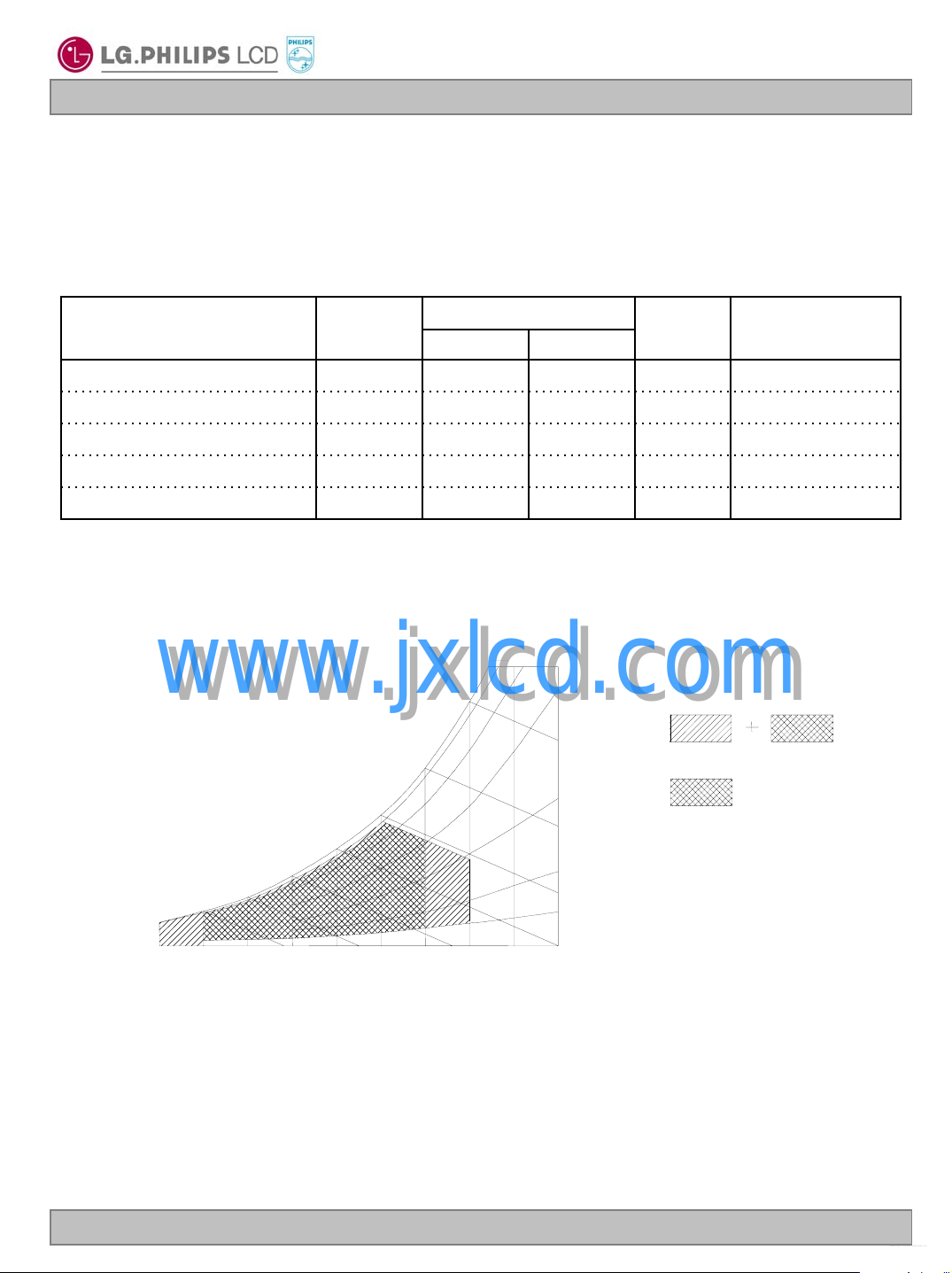
Note : 1. Temperature and relative humidity range are shown in the figure below.
Wet bulb temperature should be 39
www.jxlcd.com
www.jxlcd.com
Wet Bulb
Temperature [℃]
20
10
0
VCC -0.3 4.0 Vdc at 25 ± 5°C
TOP 050°C1
HST -20 60 °C1
HOP 10 90 %RH 1
HST 10 90 %RH 1
°C Max, and no condensation of water.
50
40
30
Values
Min Max
90% 80%
60
Units
60%
Humidity[(%)RH]
Storage
40%
Operation
20%
10%
NotesSymbol
-20
Ver. 0.0 FEB. 20, 2002
10
20 30 40 50
Dry Bulb Temperature [℃]
60 70 800
5/ 29
LP141X13(B1)
www.DataSheet.net/
Datasheet pdf - http://www.DataSheet4U.co.kr/
Liquid Crystal Display
Product Specification
3. Electrical Specifications
3-1. Electrical Characteristics
The LP141X13(B1) requires two power inputs. One is employed to power the LCD e lectronics and to drive
the TFT array and liquid crystal. The second input which powers the CCFL, is typically generated by an
inverter. The inverter is an external unit to t h e L CD.
Table 2. ELECTRICAL CHARACTERISTICS
Parameter Symbol
MODULE :
Power Supply Input Voltage VCC 3.0 3.3 3.6 V
Power Supply Input Current I
Power Consumption Pc - 1.2 1.7 Watt 1
Differential Impedance
LAMP :
Operating Voltage V
Operating Current I
Operating Frequency f
Discharge Stabilization Time Ts - - 3 Min 4
Life Time 10,000 - - Hrs 5
INVERTER :
Input Voltage V
Input Current I
Input Power Consumption P
Backlight On/Off Control FPVEE_High 2.0 - 5.25 V
Backlight Adjust (IBLControl) FF_H - 00_H Output Voltage V
Output Current (Aging 30minutes) I
Operating Frequency Freq. 45 60 75 KHz 7
Output Power Consumption P
Open Lamp Voltage V
Efficiency η 75 --%9
Striking Time T
www.jxlcd.com
www.jxlcd.com
CC
Zm
BL
BL
BL
IN
IN
IN
FPVEE_Low -0.3 - 0.8 V
OUT
_FF -2.02.3mA
OUT
I
_00 5.5 6.0 6.5 mA
OUT
OUT
OPEN
S
Min Typ Max
- 365 515 mA 1
90 100 110 Ohm 2
615(6.5mA) 630(6mA) 795(3.0mA) V
3.0 6.0 6.5 mA
50 65 80 kHz
9.0 14.4 21.0 V
- 340 390 mA 6
4.17 4.90 5.62 W 6
580 680 780 V
3.98 4.1 4.68 W 6
1450 - - V
0.6 1.0 1.4 sec 10
Values
Unit Notes
DC
RMS
RMS
DC
DC
DC
RMS
RMS
RMS
RMS
3
6
7
7
8
Note)
1. The specified current and power consumption are under the Vcc = 3.3V , 25℃, fv = 60Hz condition
whereas full black pattern is displayed and fv is the frame frequency.
2. This impedance value is needed to proper display and measured form LVDS Tx to the mating connector.
3. The typical operating current is for the typical surface luminance (L
Ver. 0.0 FEB. 20, 2002
) in optical characteristics.
WH
6/ 29
LP141X13(B1)
www.DataSheet.net/
Datasheet pdf - http://www.DataSheet4U.co.kr/
Liquid Crystal Display
Product Specification
Note)
4. Define the brightness of the lamp after being lighted for 5 minutes as 100%, Ts is the time required for
the brightness of the center of the lamp to be not less than 95%.
5. The life time is determined as the time at which brightness of lamp is 50% compare to that of initial value
at the typical lamp current.
6. V
= 14.4V, I
IN
7. V
= 9 ~ 21V.
IN
8. No Load, V
9. V
=9V, 00_H.
IN
10. No Load, V
= 6.0mA.
OUT
= 9V.
IN
= 9 ~ 21V, 00_H
IN
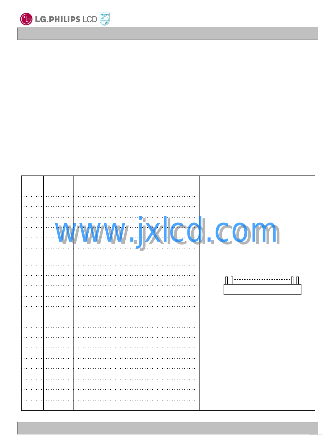
3-2. Interface Connections
This LCD employs two interface connections, a 30 pin connector is used for the module electronics interface
and the other connector is used for the integral backlight system.
The electronics interface connector is a model FI-XB30SR-HF11 manufactured by JAE.
Table 3. MODULE CONNECTOR PIN CONFIGURATION (CN1)
Pin Symbol Description Notes
1 GND Ground
2 VCC Power Supply, 3.3V Typ.
3 VCC Power Supply, 3.3V Typ.
4
V EEDID DDC 3.3V power
5
6
7
8
9
10
11
12
13
14
15
16
17
18
19
20
21~30
NC Reserved for supplier test point
www.jxlcd.com
www.jxlcd.com
Clk EEDID DDC Clock
DATA
EEDID
RIN0- Negative LVDS differential data input
RIN0+ Positive LVDS differential data input
GND Ground
R
IN
R
IN
GND Ground
RIN2- Negative LVDS differential data input
RIN2+ Positive LVDS differential data input
GND Ground
CLKIN- Negative LVDS differential clock input
CLKIN+ Positive LVDS differential clock input
GND Ground
NC No connect
NC No connect
DDC Data
1- Negative LVDS differential data input
1+ Positive LVDS differential data input
1, Interface chips
1.1 LCD : LPZE102S6L(LCD Controller)
1.2 System : THC63LVDF823A or equivalent
* Pin to Pin compatible with TI LVDS
2. Connector
2.1 LCD : FI-XB30SRL-HF11, JAE
2.2 Mating : FI-X30M or equivalent.
2.3 Conncetor pin arrangement
including LVDS Receiver
30
[LCD Module Rear View]
1
Ver. 0.0 FEB. 20, 2002
7/ 29
LP141X13(B1)
www.DataSheet.net/
Datasheet pdf - http://www.DataSheet4U.co.kr/
Liquid Crystal Display
Product Specification
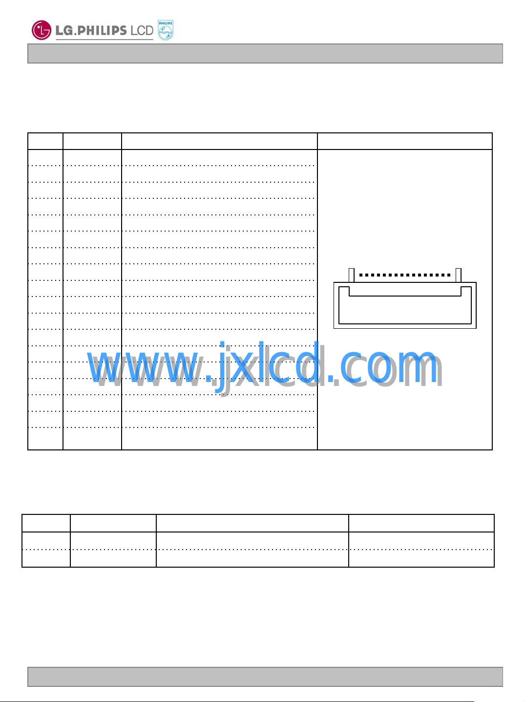
The inverter interface connector(J1) is a LVC-D20SFYG model manufactured by Honda. The pin
configuration for the connector is shown in the table below.
Table 4. BACKLIGHT INVERTER CONNECTOR PIN CONFIGURATION (J1)
Pin Symbol Description Notes
1V
2VINPower for the inverter
3V
4 NC No connection
5 GND Ground
6 5V_SUS Power for the control circuit
7 5V_ALW Power for storing a brightness values
8 GND Ground
9 SMB_DAT Brightness data
10 SMB_CLK Clock for brightness data
11 GND Ground
12 FPVEE Enable for lamp turn on and off
13 GND Ground
14~16 NC No connection
17 PANEL_ID3 1(OPEN)
18 PANEL_ID2 1(OPEN)
19 PANEL_ID1 1(OPEN)
IN
IN
www.jxlcd.com
www.jxlcd.com
Power for the inverter
Power for the inverter
[Connector]
LVC-D20SFYG, Honda
[Connector pin arrangement]
120
20 PANEL_ID0 1(OPEN)
The backlight interface connector is a model BHSR-02VS-1, manufactured by JST. The mating connector
part number is SM02B-BHSS-1 or equivalent.
Table 5. BACKLIGHT CONNECTOR PIN CONFIGURATION (J3)
NotesDescriptionSymbolPin
1Power supply for lamp (High voltage side)HV1
1Power supply for lamp (Low voltage side)LV2
Notes : 1. The high voltage side terminal is colored pink and the low voltage side terminal is white
Ver. 0.0 FEB. 20, 2002
8/ 29
LP141X13(B1)
www.DataSheet.net/
Datasheet pdf - http://www.DataSheet4U.co.kr/
Liquid Crystal Display
Product Specification
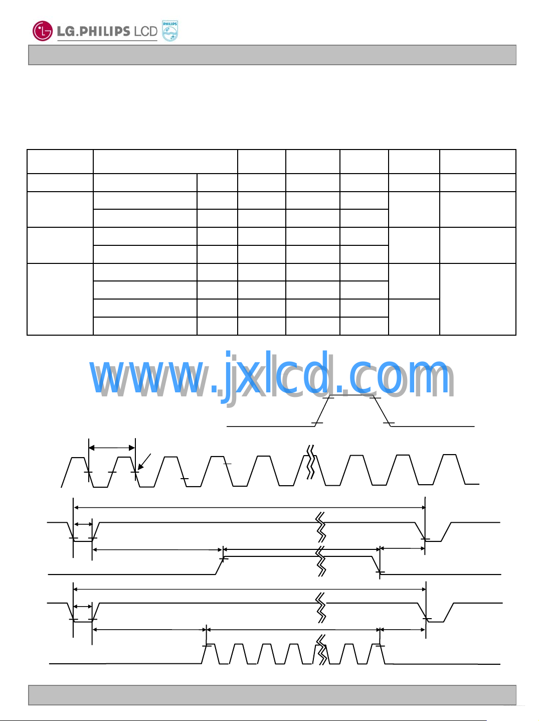
3-3. Signal Timing Specifications
This is the signal timing required at the input of the User connector. All of the interface signal timing should be
satisfied with the following specifications and specifications of LVDS Tx/Rx for it’s proper operation.
Table 6. TIMING TABLE
ITEM Symbol Min Typ Max Unit Note
DCLK Frequency fCLK 65 65 65 MHz 15.4ns
Hsync
Vsync
Data
Enable
Period t
Width tWH 8 136 240
Period t
Width t
Horizontal back porch tHBP 16 - -
Horizontal front porch tHFP 16 - -
Vertical back porch t
Vertical front porch tVFP 2--
3-4. Signal Timing Waveforms
www.jxlcd.com
www.jxlcd.com
Data Enable, Hsync, Vsy n c
DCLK
tCLK
0.5 Vcc
HP 1206 1344 1364
VP 780 806 830
WV 2- -
VBP 3--
Condition : VCC =3.3V
High: 0.7VCC
Low: 0.3VCC
CLK
t
t
CLK
t
t
HP
HP
t
Hsync
Data Enable
Vsync
Ver. 0.0 FEB. 20, 2002
t
WH
t
WV
Data Enable
t
VBP
t
HBP
HP
t
tWHA
VP
tWVA
t
HFP
t
VFP
9/ 29
 Loading...