

LG LP-141WX3-TLP1 Service manual
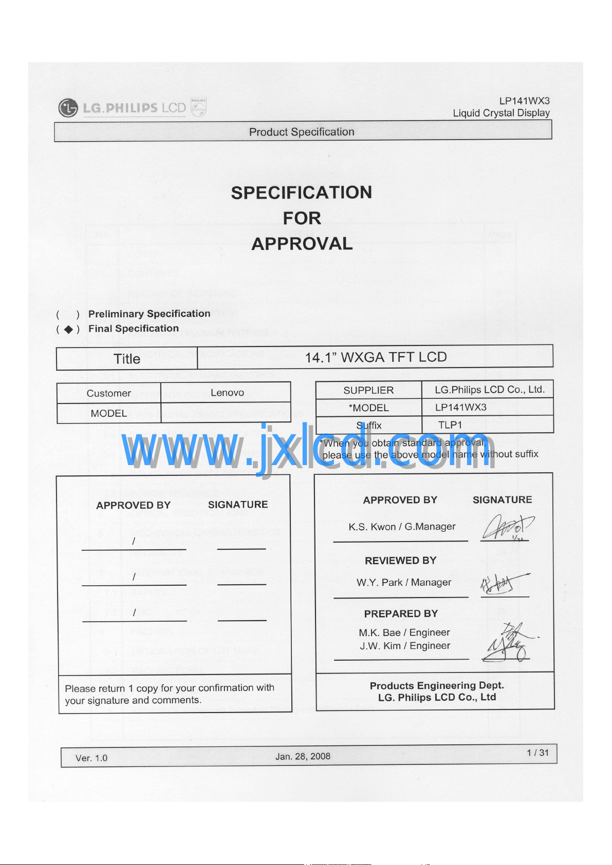
Product Specification
LP141WX3
Liquid Crystal Display
www.jxlcd.com
www.jxlcd.com
Ver. 1.0 Jan. 28, 2008
0 / 31
LP141WX3
Liquid Crystal Display
Product Specification
SPECIFICATION
FOR
APPROVAL
)
(
(
Preliminary Specification
)
Final Specification
◆
14.1” WXGA TFT LCDTitle
LenovoCustomer
MODEL
*When you obtain standard approval,
www.jxlcd.com
www.jxlcd.com
SIGNATUREAPPROVED BY
/
/
/
please use the above model name without suffix
APPROVED BY
K.S. Kwon / G.Manager
REVIEWED BY
W.Y. Park / Manager
PREPARED BY
M.K. Bae / Engineer
J.W. Kim / Engineer
LG.Philips LCD Co., Ltd.SUPPLIER
LP141WX3*MODEL
TLP1Suffix
SIGNATURE
Please return 1 copy for your confirmation with
your signature and comments.
Ver. 1.0 Jan. 28, 2008
Products Engineering Dept.
LG. Philips LCD Co., Ltd
1 / 31
Product Specification
Contents
LP141WX3
Liquid Crystal Display
ITEMNo
COVER
CONTENTS
RECORD OF REVISIONS
GENERAL DESCRIPTION1
ABSOLUTE MAXIMUM RATINGS2
ELECTRICAL SPECIFICATIONS3
ELECTRICAL CHARACTREISTICS3-1
INTERFACE CONNECTIONS3-2
LVDS SIGNAL TIMING SPECIFICATIONS3-3
SIGNAL TIMING SPECIFICATIONS3-4
SIGNAL TIMING WAVEFORMS3-5
www.jxlcd.com
www.jxlcd.com
COLOR INPUT DATA REFERNECE3-6
POWER SEQUENCE3-7
OPTICAL SFECIFICATIONS4
Page
1
2
3
4
5
6
8
9
11
11
12
13
14
MECHANICAL CHARACTERISTICS5
RELIABLITY6
INTERNATIONAL STANDARDS7
SAFETY7-1
EMC7-2
PACKING8
DESIGNATION OF LOT MARK8-1
PACKING FORM8-2
PRECAUTIONS9
APPENDIX. Enhanced Extended Display Identification Data A
Ver. 1.0 Jan. 28, 2008
17
24
25
25
26
26
27
29
2 / 31
Product Specification
RECORD OF REVISIONS
LP141WX3
Liquid Crystal Display
DescriptionPageRevision DateRevision No
First Draft (Preliminary Specification)-Oct. 15. 20070.0
Table 4. BACKLIGHT CONNECTOR PIN CONFIGURATION (J3)8Dec. 29. 20070.2
-Be updated high voltage side terminal color (Pink → White)
Be updated Color Coordinates14
15
www.jxlcd.com
www.jxlcd.com
Be updated Gray scale specification
Final CASJan. 28. 20081.0
EDID
ver
0.1
0.2EDID update(be uadated product code)29~31Dec. 13. 20070.1
Ver. 1.0 Jan. 28, 2008
3 / 31
LP141WX3
Liquid Crystal Display
Product Specification
1. General Description
The LP141WX3 is a Color Active Matrix Liquid Crystal Display with an integral Cold Cathode Fluorescent
Lamp (CCFL) backlight system. The matrix employs a-Si Thin Film Transistor as the active element. It is a
transmissive type display operating in the normally white mode. This TFT-LCD has 14.1 inches diagonally
measured active display area with WXGA resolution(800 vertical by 1280 horizontal pixel array). Each pixel
is divided into Red, Green and Blue sub-pixels or dots which are arranged in vertical stripes. Gray scale or
the brightness of the sub-pixel color is determined with a 6-bit gray scale signal for each dot, thus,
presenting a palette of more than 262,144 colors.
The LP141WX3 has been designed to apply the interface method that enables low power, high speed, low
EMI.
The LP141WX3 is intended to support applications where thin thickness, low power are critical factors and
graphic displays are important. In combination with the vertical arrangement of the sub-pixels, the
LP141WX3 characteristics provide an excellent flat display for office automation products such as Notebook
PC.
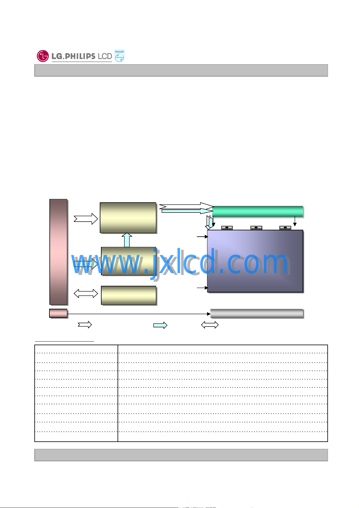
CN
1
User connector
www.jxlcd.com
www.jxlcd.com
30
Pin
CN
General Features
Outline Dimension
LVDS &
Timing
Control
Block
POWER
BLOCK
EDID
BLOCK
Control & Data Power EDID signal & Power
14.1 inches diagonal Active Screen Size
319.5(H,Typ.) × 205.5(V,Typ.) × 5.5(D,Max) [mm]
0.2373mm × 0.2373 mmPixel Pitch
1280 horiz. By 800 vert. Pixels RGB strip arrangementPixel Format
6-bit, 262,144 colorsColor Depth
200 cd/m2(Typ.5 point)Luminance, White
Total 5.2 Watt(Typ.) @ LCM circuit 1.2 Watt(Typ._Mosaic), B/L input 4.0Watt(Typ.)Power Consumption
400g(Max.) Weight
Transmissive mode, normally whiteDisplay Operating Mode
Anti glare treatment of the front polarizerSurface Treatment
YesRoHS Comply
1
GIP(Gate In Panel)
800
Source Driver Circuit
1
TFT-LCD Panel
(1280 x 800)
Backlight Ass’y
1280
Ver. 1.0 Jan. 28, 2008
4 / 31
LP141WX3
Liquid Crystal Display
Product Specification
2. Absolute Maximum Ratings
The following are maximum values which, if exceeded, may cause faulty operation or damage to the unit.
Table 1. ABSOLUTE MAXIMUM RATINGS
60
Values
Units
MaxMin
90% 80%
60%
Humidity[(%)RH]
Storage
40%
Operation
20%
10%
Parameter Notes
Power Input Voltage
Operating Temperature
Storage Temperature
Operating Ambient Humidity
Storage Humidity
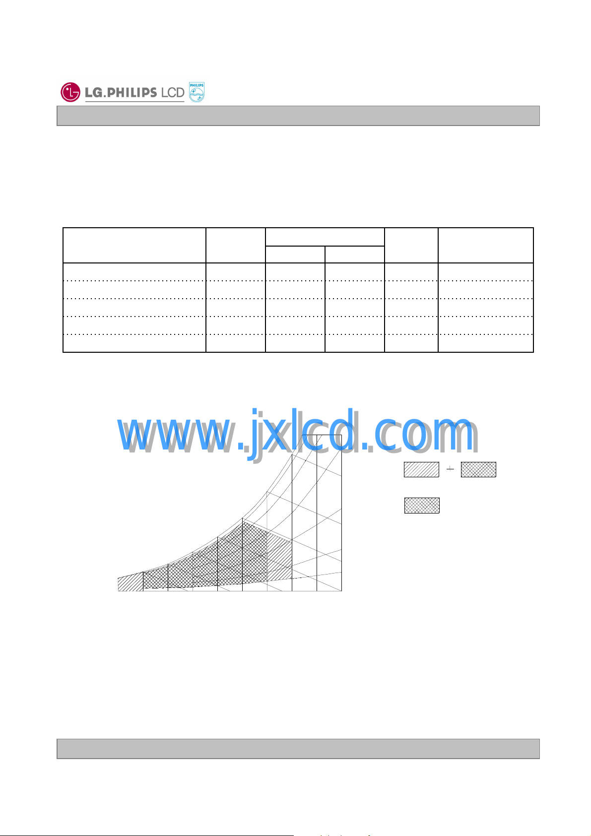
Note : 1. Temperature and relative humidity range are shown in the figure below.
Wet bulb temperature should be 39°C Max, and no condensation of water.
www.jxlcd.com
www.jxlcd.com
Wet Bulb
Temperature [℃℃℃℃]
20
10
0
Symbol
50
40
30
at 25 ± 5°CVdc4.0-0.3VCC
1°C500TOP
1°C60-20HST
1%RH9010HOP
1%RH9010HST
-20
Ver. 1.0 Jan. 28, 2008
10
20 30 40 50
Dry Bulb Temperature [℃℃℃℃]
60 70 800
5 / 31
LP141WX3
Liquid Crystal Display
Product Specification
3. Electrical Specifications
3-1. Electrical Characteristics
The LP141WX3 requires two power inputs. One is employed to power the LCD electronics and to drive the
TFT array and liquid crystal. The second input which powers the CCFL, is typically generated by an
inverter. The inverter is an external unit to the LCD.
Table 2. ELECTRICAL CHARACTERISTICS
Parameter Symbol
MODULE :
LAMP :
Operating Voltage
Operating Current
Power Consumption
Operating Frequency
www.jxlcd.com
www.jxlcd.com
Established Starting Voltage
at 25℃
at 0 ℃
I
CC
Mosaic
BL
BL
BL
BL
Vs
1180
1415
Values
DC
RMS
NotesUnit
1mA414360-Mosaic
1Watt1.41.2-PcPower Consumption
2Ohm11010090ZmDifferential Impedance
3mA
4Min3TsDischarge Stabilization Time
5Hrs15,000Life Time
MaxTypMin
3.63.33.0VCCPower Supply Input Voltage
880(2.0mA)670(6.0mA)640(7.0mA)V
7.06.02.0I
V
V
RMS
W4.54.01.8P
kHz805545f
V
RMS
V
RMS
Note)
1. The specified current and power consumption are under the Vcc = 3.3V , 25℃, fv = 60Hz condition
whereas Mosaic pattern is displayed and fv is the frame frequency.
2. This impedance value is needed to proper display and measured form LVDS Tx to the mating connector.
3. The typical operating current is for the typical surface luminance (LWH) in optical characteristics.
4. Define the brightness of the lamp after being lighted for 5 minutes as 100%, Ts is the time required for
the brightness of the center of the lamp to be not less than 95%.
5. The life time is determined as the time at which brightness of lamp is 50% compare to that of initial value
at the typical lamp current.
Ver. 1.0 Jan. 28, 2008
6 / 31
LP141WX3
Liquid Crystal Display
Product Specification
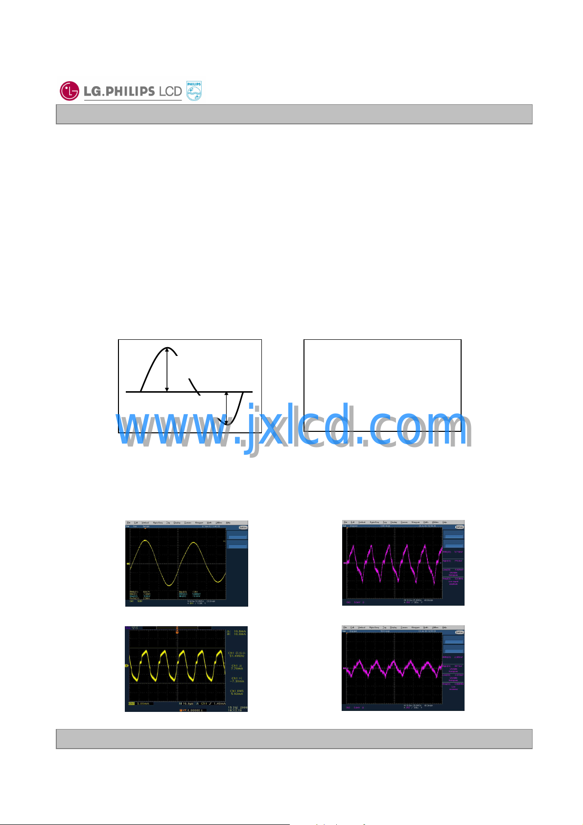
Note)
6. The output of the inverter must have symmetrical(negative and positive) voltage waveform and
symmetrical current waveform.(Asymmetrical ratio is less than 10%) Please do not use the inverter
which has asymmetrical voltage and asymmetrical current and spike wave.
Lamp frequency may produce interface with horizontal synchronous frequency and as a result this may
cause beat on the display. Therefore lamp frequency shall be as away possible from the
horizontal synchronous frequency and from its harmonics in order to prevent interference.
7. It is defined the brightness of the lamp after being lighted for 5 minutes as 100%.
TSis the time required for the brightness of the center of the lamp to be not less than 95%.
8. The lamp power consumption shown above does not include loss of external inverter.
The applied lamp current is a typical one.
9. Requirements for a system inverter design, which is intended to have a better display performance, a
better power efficiency and a more reliable lamp, are following.
It shall help increase the lamp lifetime and reduce leakage current.
a. The asymmetry rate of the inverter waveform should be less than 10%.
b. The distortion rate of the waveform should be within √2 ±10%.
* Inverter output waveform had better be more similar to ideal sine wave.
* Asymmetry rate:
I p
| I p– I –p| / I
rms
* 100%
I -p
10. Inverter open voltage must be more than lamp voltage for more than 1 second for start-up.
Otherwise, the lamps may not be turned on.
※ Do not attach a conducting tape to lamp connecting wire.
If the lamp wire attach to a conducting tape, TFT-LCD Module has a low luminance and the inverter
has abnormal action. Because leakage current is occurred between lamp wire and conducting tape.
Ex of current wave)
www.jxlcd.com
www.jxlcd.com
Normal current wave - Standard
* Distortion rate
I p(or I –p) / I
Abnormal current wave - Bad
rms
Abnormal current wave - Bad
Ver. 1.0 Jan. 28, 2008
Abnormal current wave - Bad
7 / 31
LP141WX3
Liquid Crystal Display
Product Specification
3-2. Interface Connections
This LCD employs two interface connections, a 30 pin connector is used for the module electronics interface
and the other connector is used for the integral backlight system.
The electronics interface connector is a model GT101-30S-HR11 manufactured by LSC.
Table 3. MODULE CONNECTOR PIN CONFIGURATION (CN1)
NotesDescriptionSymbolPin
GroundGND1
Power Supply, 3.3V Typ.VCC2
Power Supply, 3.3V Typ.VCC3
DDC 3.3V powerV EEDID4
Reserved for supplier test pointNC5
DDC ClockClk EEDID6
DDC DataDATA EEDID7
Negative LVDS differential data inputRIN0-8
Positive LVDS differential data inputRIN0+9
GroundGND10
Negative LVDS differential data inputRIN1-11
Positive LVDS differential data inputRIN1+12
GroundGND13
Negative LVDS differential data inputRIN2-14
Positive LVDS differential data inputRIN2+15
GroundGND16
Negative LVDS differential clock inputCLKIN-17
www.jxlcd.com
www.jxlcd.com
NC No Connect21
Positive LVDS differential clock inputCLKIN+18
GroundGND19
No ConnectNC20
GroundGND22
No ConnectNC23
No ConnectNC24
GroundGND25
No ConnectNC26
No ConnectNC27
GroundGND28
No ConnectNC29
No ConnectNC30
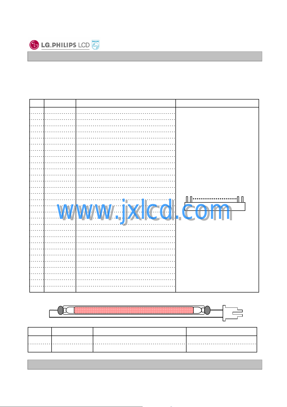
The backlight interface connector is a model BHSR-02VS-1, manufactured by JST or Compatible.
The mating connector part number is AMP1674817-2 or equivalent.
Table 4. BACKLIGHT CONNECTOR PIN CONFIGURATION (J3)
1, Interface chips
1.1 LCD : SW, SW0612B (LCD Controller)
including LVDS Receiver
1.2 System : THC63LVD823A or equivalent
* Pin to Pin compatible with LVDS
2. Connector
2.1 LCD : GT101-30S-HR11, LSC
IS100-C30R-C15 ,UJU Elec.
2.2 Mating : FI-X30M or equivalent.
2.3 Connector pin arrangement
30
it’s compatible.
1
[LCD Module Rear View]
PIN1
PIN2PIN2
NotesDescriptionSymbolPin
1Power supply for lamp (High voltage side)HV1
1Power supply for lamp (Low voltage side)LV2
Notes : 1. The high voltage side terminal is colored Pink and the low voltage side terminal is Yellow.
Ver. 1.0 Jan. 28, 2008
8 / 31
Product Specification
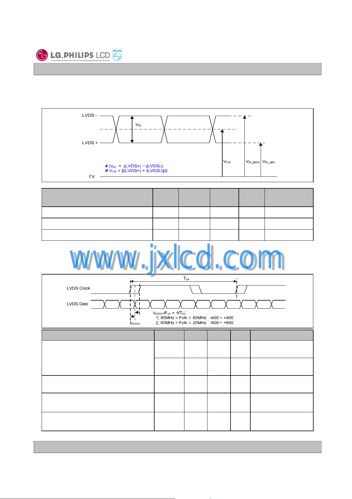
3-3. LVDS Signal Timing Specifications
3-3-1. DC Specification
LP141WX3
Liquid Crystal Display
Description
LVDS Common mode Voltage
LVDS Input Voltage Range
3-3-2. AC Specification
LVDS Clock to Data Skew Margin
www.jxlcd.com
www.jxlcd.com
Symb
ol
CM
IN
SKEW
SKEW
- 600
NotesUnitMaxMin
-mV600100|VID|LVDS Differential Voltage
-V1.80.6V
-V2.10.3V
NotesUnitMaxMinSymbolDescription
ps+ 400- 400t
ps+ 600t
85MHz > Fclk ≥
65MHz
65MHz > Fclk ≥
25MHz
LVDS Clock to Clock Skew Margin (Even
to Odd)
Maximum deviation
of input clock frequency during SSC
Maximum modulation frequency
of input clock during SSC
Ver. 1.0 Jan. 28, 2008
SKEW_EO
DEV
MOD
- 1/7
+ 1/7t
T
clk
%± 3-F
KHz200-F
-
-
-
9 / 31
 Loading...