

LG LP-141WP2-TLB1 Service manual
LP141WP2
Liquid Crystal Display
Product Specification
SPECIFICATION
FOR
APPROVAL
)
(
(
Preliminary Specification
)
Final Specification●
14.1” WXGA+ TFT LCDTitle
LenovoBUYER
Malibu-3MODEL
*When you obtain standard approval,
www.jxlcd.com
www.jxlcd.com
APPROVED BY
/
/
/
SIGNATURE
please use the above model name without suffix
APPROVED BY SIGNATURE
K. J. Kwon / S.Manager
REVIEWED BY
G. J. Han / Manager
PREPARED BY
K. Y. Kwon / Engineer
LP141WP2*MODEL
TLB1Suffix
LG Display Co., Ltd.SUPPLIER
Please return 1 copy for your confirmation with
your signature and comments.
Ver. 1.1 22, Apr, 2008
Product Engineering Dept.
LG Display Co., Ltd
0/ 31
Product Specification
Contents
LP141WP2
Liquid Crystal Display
ITEMNo
CONTENTS
RECORD OF REVISIONS
GENERAL DESCRIPTION1
ABSOLUTE MAXIMUM RATINGS2
ELECTRICAL SPECIFICATIONS3
ELECTRICAL CHARACTREISTICS 3-1
INTERFACE CONNECTIONS 3-2
SIGNAL TIMING SPECIFICATIONS 3-3
SIGNAL TIMING WAVEFORMS 3-4
COLOR INPUT DATA REFERNECE 3-5
POWER SEQUENCE 3-6
www.jxlcd.com
www.jxlcd.com
OPTICAL SFECIFICATIONS4
MECHANICAL CHARACTERISTICS5
RELIABLITY6
Page
1
2
3
4
5
6
8
10
11
12
13
16
20
INTERNATIONAL STANDARDS7
SAFETY 7-1
EMC 7-2
PACKING8
DESIGNATION OF LOT MARK 8-1
PACKING FORM 8-2
PRECAUTIONS9
Ver. 1.1 22, Apr, 2008
21
21
22
22
23
1/ 31
Product Specification
RECORD OF REVISIONS
LP141WP2
Liquid Crystal Display
DescriptionPageRevision DateRevision No
First Draft (Preliminary Specification)-1. Oct. 20070.0
Change pixel strip structure (BGRRGB)313. Mar. 20080.1
Update LED Backlight Spec.5
Update LED PWM Spec.526. Mar. 20080.2
Update Signal Timing Spec. for WWAN10
Update EDID Data29~31
Update LED Backlight Spec.514. Apr. 20081.0
Final SpecificationUpdate Timing table1022. Apr. 20081.1
T4 timing change (2000)12
www.jxlcd.com
www.jxlcd.com
EDID
ver
0.0
1.3Update EDID Data29~31
1.4
Ver. 1.1 22, Apr, 2008
2/ 31
LP141WP2
Liquid Crystal Display
Product Specification
1. General Description
The LP141WP2 is a Color Active Matrix Liquid Crystal Display with an integral LED backlight system. The
matrix employs a-Si Thin Film Transistor as the active element. It is a transmissive type display operating in
the normally white mode. This TFT-LCD has 14.1 inches diagonally measured active display area with
WXGA+ resolution(1440 horizontal by 900 vertical pixel array). Each pixel is divided into Red, Green and
Blue sub-pixels or dots which are arranged in vertical stripes. Gray scale or the brightness of the sub-pixel
color is determined with a 6-bit gray scale signal for each dot, thus, presenting a palette of more than
262,144 colors.
The LP141WP2 has been designed to apply the interface method that enables low power, high speed, low
EMI.
The LP141WP2 is intended to support applications where thin thickness, low power are critical factors and
graphic displays are important. In combination with the vertical arrangement of the sub-pixels, the
LP141WP2 characteristics provide an excellent flat display for office automation products such as Notebook
PC.
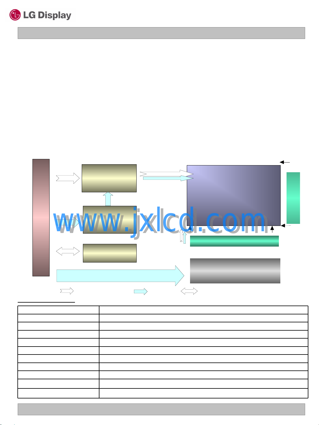
CN1 User connector 40 Pin
www.jxlcd.com
www.jxlcd.com
FI-JT40S
General Features
LVDS &
Timing
Control
Block
POWE
R
BLOCK
EDID
BLOCK
VBL+ & PWM
Control & Data Power EDID signal & Power
14.1 inches diagonal Active Screen Size
319.5 (H) × 206.5 (V) × 5.5(D, max.) mmOutline Dimension
0.2106 mm × 0.2106 mm Pixel Pitch
1440 horiz. by 900 vert. Pixels RGB strip arrangementPixel Format
6-bit, 262,144 colorsColor Depth
250 cd/m2(Typ., @I
Total 4.61Watt @ LCM circuit 1.42W(Typ.), B/L 2.59 W (Typ.), LED Driver 0.6W(Typ.)Power Consumption
360g(Max.)Weight
Transmissive mode, normally whiteDisplay Operating Mode
Haze44% (ARC150T)Surface Treatment
YesRoHS Comply
LED
=15mA) , 5 points Average Luminance, White
TFT-LCD Panel
(1440 x 900)
Source Driver Circuit
LED Backlight Ass’y
9LEDs X 6 strings
1440
1
Gate In Panel
9001
Ver. 1.1 22, Apr, 2008
3/ 31

LP141WP2
Liquid Crystal Display
Product Specification
2. Absolute Maximum Ratings
The following are maximum values which, if exceeded, may cause faulty operation or damage to the unit.
Table 1. ABSOLUTE MAXIMUM RATINGS
Parameter Notes
Power Input Voltage
Operating Temperature
Storage Temperature
Operating Ambient Humidity
Storage Humidity
Note : 1. Temperature and relative humidity range are shown in the figure below.
Wet bulb temperature should be 39C Max, and no condensation of water.
www.jxlcd.com
www.jxlcd.com
Wet Bulb
Temperature [℃]
20
10
0
Symbol
60
50
40
30
Values
MaxMin
90% 80%
60%
40%
20%
10%
Units
Humidity[(%)RH]
Storage
Operation
at 25 5CVdc4.0-0.3VCC
1C500TOP
1C60-20HST
1%RH9010HOP
1%RH9010HST
-20
Ver. 1.1 22, Apr, 2008
10
20 30 40 50
Dry Bulb Temperature [℃]
60 70 800
4/ 31
LP141WP2
Liquid Crystal Display
Product Specification
3. Electrical Specifications
3-1. Electrical Characteristics
The LP141WP2 requires two power inputs. One is employed to power the LCD electronics and to drive the
TFT array and liquid crystal. The second input which powers the LED BLU.
Table 2. ELECTRICAL CHARACTERISTICS
Parameter Symbol
MODULE :
Power Supply Input Current
(Window desktop pattern)
Power Consumption
(Window desktop pattern)
LED Backlight :
Operating Voltage
Operating Current per string
Power Consumption (dimming 100%)
LED Driver power consumption
www.jxlcd.com
www.jxlcd.com
PWM input signal :
CC
LED
LED
BL
Driver
Values
MaxTypMin
3.63.33.0VCC Power Supply Input Voltage
V
Hz230225220- Input Frequency (for wavy)
NotesUnit
DC
1mA495430365I
1Watt1.631.42-Pc
2Ohm11010090Zm Differential Impedance
3V30.628.8-V
4mA-15-I
-Watt2.752.59-P
-Watt-0.6-P
5Hrs--10,000 Life Time
V26157BL_VCC BL Input Voltage
6Hz500-100- Input Frequency (for operating)
V--2.1- on threshold
V0.8--- off threshold
7, 8%100-12.5- Duty Cycle
Note)
1. The specified current and power consumption are under the Vcc = 3.3V , 25℃, fv = 60Hz condition
whereas Window desktop pattern is displayed and fv is the frame frequency.
2. This impedance value is needed to proper display and measured form LVDS Tx to the mating connector.
3. The variance of the voltage is ± 10%.
4. The typical operating current is for the typical surface luminance (LWH) in optical characteristics.
I
5. The life time is determined as the time at which brightness of LED is 50% compare to that of initial value
at the typical LED current.
6. LED Driver operating Frequency
7. There may be a flickering Under 6% dimming.
8. There is no reliability issue. (Under 12.5% duty cycle)
9. There is no reliability issue beyond input frequency 220 ~ 230. It is optimized frequency for wavy noise.
is the current of each LEDs’ string, LED backlight has 6 strings on it.
LED
Ver. 1.1 22, Apr, 2008
5/ 31
LP141WP2
Liquid Crystal Display
Product Specification
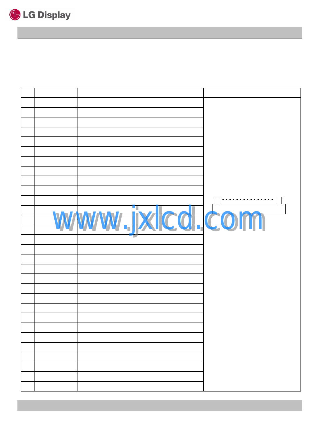
3-2. Interface Connections
This LCD employs two interface connections, a 40 pin connector is used for the module electronics interface
and the other connector is used for the internal backlight system.
The electronics interface connector is a model FI-JT40S manufactured by JAE.
Table 3. MODULE CONNECTOR PIN CONFIGURATION (CN1)
Pin
1
2
3
4
5
6
7
8
9
10
11
12
13
14
15
16
17
18
19
20
21
22
23
24
25
26
27
28
29
30
DescriptionSymbol
Ground/Connector testVSS
Power Supply(3.3V typ.)VDD
Power Supply(3.3V typ.)VDD
Power Supply(3.3V typ.)VDD
DDC 3.3V powerV_EDID
DDC ClockCLK_EDID
DDC DataDATA_EDID
Negative LVDS differential data input Odd_Rin0Positive LVDS differential data input Odd_Rin0+
VSS1
www.jxlcd.com
www.jxlcd.com
Ground
Negative LVDS differential data input Odd_Rin1Positive LVDS differential data input Odd_Rin1+
GroundVSS2
Negative LVDS differential data input Odd_Rin2Positive LVDS differential data input Odd_Rin2+
GroundVSS3
Negative LVDS differential clock input Odd_ClkINPositive LVDS differential clock inputOdd_ClkIN+
GroundVSS4
Negative LVDS differential data input Even_Rin0Positive LVDS differential data inputEven_Rin0+
GroundVSS5
Negative LVDS differential data inputEven_Rin1Positive LVDS differential data inputEven_Rin1+
GroundVSS6
Negative LVDS differential data inputEven_Rin2Positive LVDS differential data inputEven_Rin2+
GroundVSS7
Negative LVDS differential clock inputEven_ClkINPositive LVDS differential clock inputEven_ClkIN+
1, Interface chips
1.1 LCD : SiW, ST2_BS (LCD Controller)
including LVDS Receiver
1.2 System :
* Pin to Pin compatible with LVDS
2.Connector
2.1 LCD :JAE FI-JT40S
(1.0 mm thickness, lock-in type)
2.2 Mating:JAE FI-JT40 series or
equivalent
2.3 Connector pin arrangement
LCD rear view
40
[LCD Module Rear View]
Notes
1
Ver. 1.1 22, Apr, 2008
6/ 31
Product Specification
LP141WP2
Liquid Crystal Display
31
32
33
34
35
36
37
38
39
40
Note1)
BL_ON voltage supply more than 0.8V.
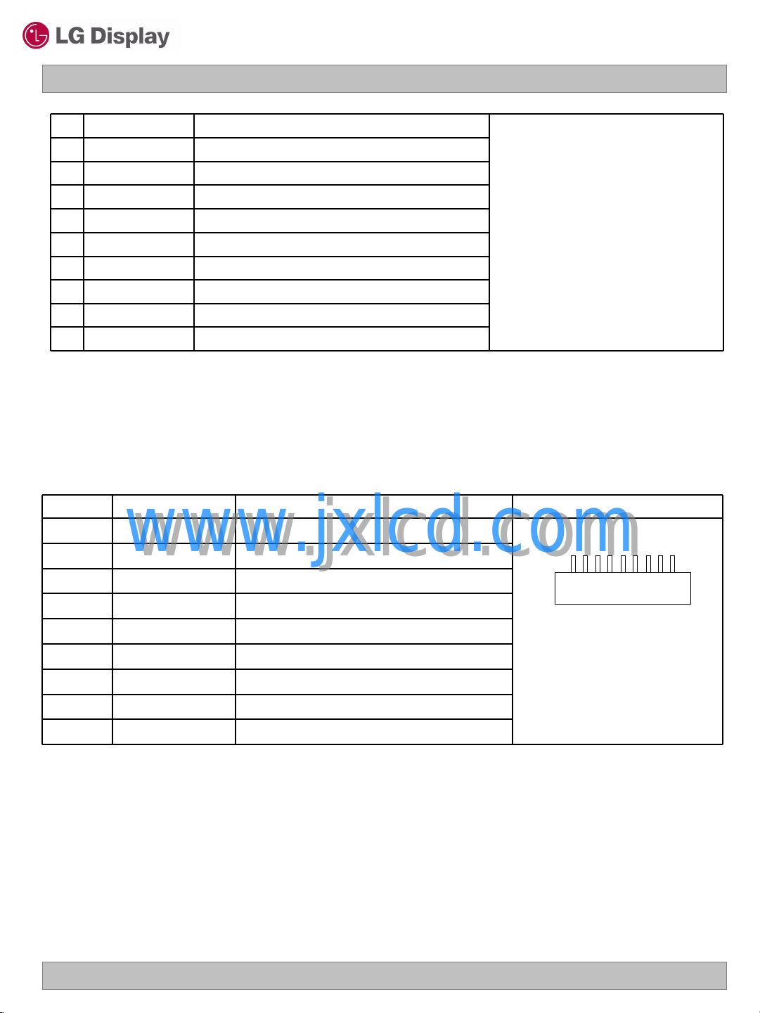
The LED backlight connector is a model TF12-9S-0.5H, manufactured by Hirose.
1
2
Vdc(1,2,3,4,5,6)
www.jxlcd.com
www.jxlcd.com
Vdc(1,2,3,4,5,6)
Backlight On/Off ControlBL_ON
PWM for luminance controlBL_PWM
GroundVSS
7V ~ 26V LED powerBL_VCC
7V ~ 26V LED powerBL_VCC
7V ~ 26V LED powerBL_VCC
LED power returnBL_VSS
LED power returnBL_VSS
LED power returnBL_VSS
No connectionNC
Table 4. BACKLIGHT CONNECTOR PIN CONFIGURATION (CN2)
LED Anode(Positive)
LED Anode(Positive)
No ConnectionNC3
NotesDescriptionSymbolPin
1
9
4
5
6
7
8
9
Ver. 1.1 22, Apr, 2008
Vdc1
Vdc2
Vdc3
Vdc4
Vdc5
Vdc6
LED Cathode (Negative)
LED Cathode (Negative)
LED Cathode (Negative)
LED Cathode (Negative)
LED Cathode (Negative)
LED Cathode (Negative)
7/ 31
Product Specification
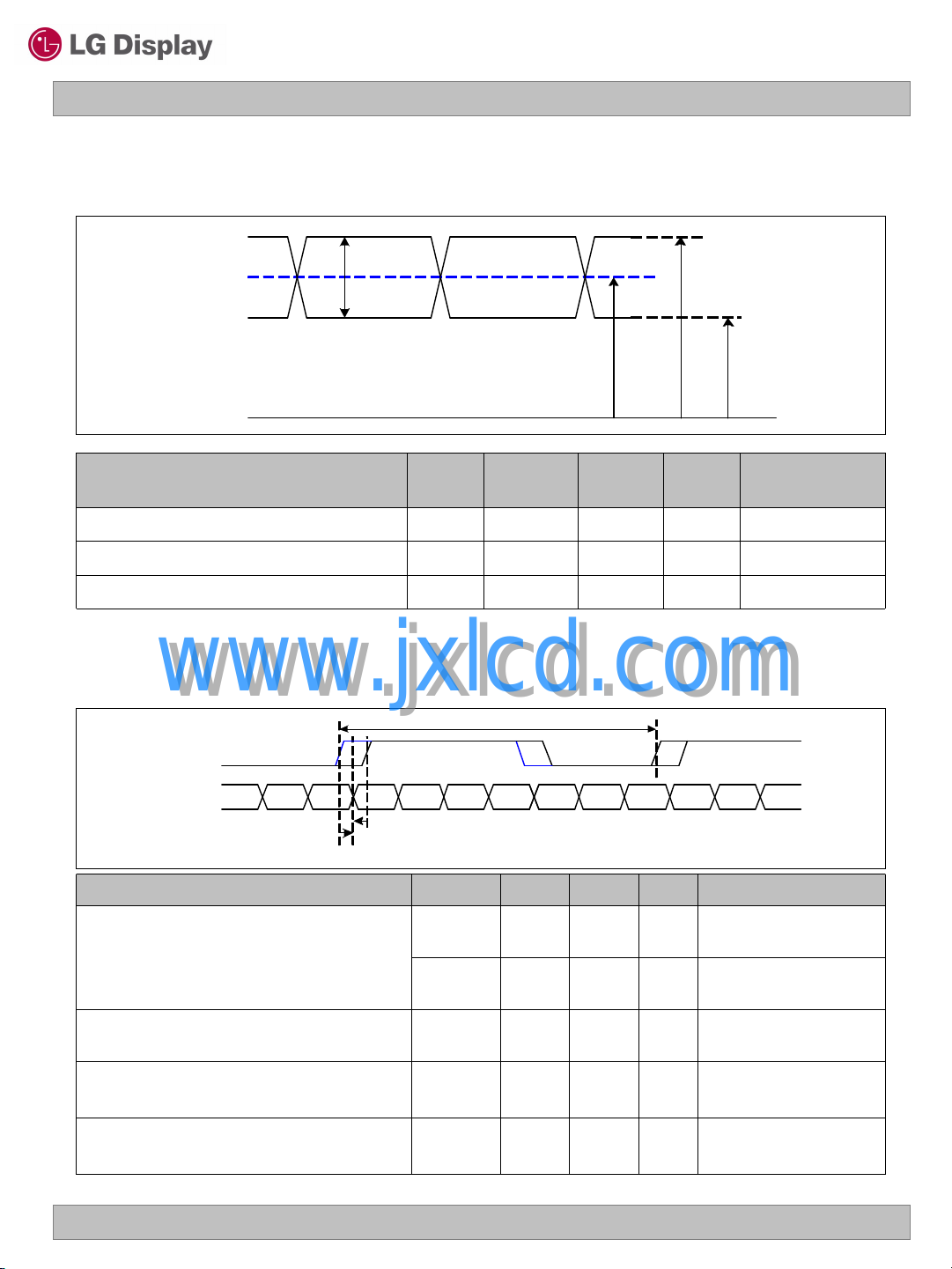
LVDS +
LVDS -
0V
V
CM
# |VID| = |(LVDS +) – (LVDS -)|
# VCM= {(LVDS +) + ( LVDS -)}/2
|VID|
V
IN_MAXVIN_MIN
LVDS Data
t
SKEW
LVDS Clock
T
clk
t
SKEW (Fclk
= 1/T
clk
)
1) 85MHz > Fclk ≥ 65MHz : -400 ~ +400
2) 65MHz > Fclk ≥ 25MHz : -600 ~ +600
3-3. LVDS Signal Timing Specifications
3-3-1. DC Specification
LP141WP2
Liquid Crystal Display
Description
LVDS Common mode Voltage
LVDS Input Voltage Range
3-3-2. AC Specification
www.jxlcd.com
www.jxlcd.com
LVDS Clock to Data Skew Margin
Symbo
l
CM
IN
SKEW
SKEW
NotesUnitMaxMin
-mV600100|VID|LVDS Differential Voltage
-V1.80.6V
-V2.10.3V
NotesUnitMaxMinSymbolDescription
ps+ 400 400-t
600-
ps+ 600t
85MHz > Fclk ≥
65MHz
65MHz > Fclk ≥
25MHz
LVDS Clock to Clock Skew Margin (Even
to Odd)
Maximum deviation
of input clock frequency during SSC
Maximum modulation frequency
of input clock during SSC
Ver. 1.1 22, Apr, 2008
SKEW_EO
DEV
MOD
- 1/7
+ 1/7t
T
clk
%± 3-F
KHz200-F
-
-
-
8/ 31
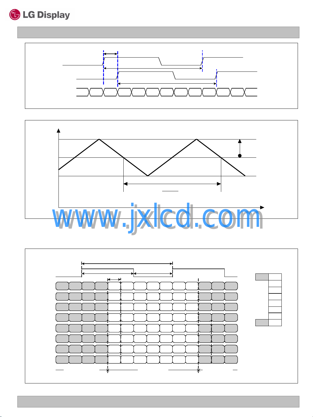
LVDS Even Data
LVDS Odd Clock
LVDS Even Clock
t
SKEW_EO
T
clk
T
clk
OG0 OR5 OR4 OR3 OR2 OR1 OR0
OB1 OB0 OG5 OG4 OG3 OG2 OG1
DE VSYNC HSYNC OB5 OB4 OB3 OB2
X OB7 OB6 OG7 OG6 OR7 OR6
Current(Nth) CyclePrevious(N-1)th Cycle Next(N+1)th Cycle
RCLK +
RXinO0 +/-
Tclk * 4/7 Tclk * 3/7
Tclk
Tclk * 1/7
MSB R7
R6
R5
R4
R3
R2
R1
R0LSB
EG0 ER5 ER4 ER3 ER2 ER1 ER0
EB1 EB0 EG5 EG4 EG3 EG2 EG1
DE
VSYNC HSYNC
EB5 EB4 EB3 EB2
X EB7 EB6 EG7 EG6 ER7 ER6
* ODD = 1st Pixel
EVEN = 2nd Pixel
RXinO1 +/-
RXinO2 +/-
RXinO3 +/-
RXinE0 +/-
RXinE1 +/-
RXinE2 +/-
RXinE3 +/-
OR3 OR2 OR1 OR0
OG4 OG3 OG2 OG1
OB5 OB4 OB3 OB2
OG7 OG6 OR7 OR6
ER3 ER2 ER1 ER0
EG4 EG3 EG2 EG1
EB5 EB4 EB3 EB2
EG7 EG6 ER7 ER6
OG0 OR5 OR4
OB1 OB0 OG5
DE VSYNC HSYNC
X OB7 OB6
EG0 ER5 ER4
EB1 EB0 EG5
DE
VSYNC HSYNC
X EB7 EB6
Freq.
F
max
F
center
F
min
Product Specification
< Clock skew margin between channel >
LP141WP2
Liquid Crystal Display
F
* F
center
DEV
3-3-3. Data Format
- LVDS 2 Port
Ver. 1.1 22, Apr, 2008
www.jxlcd.com
www.jxlcd.com
< Spread Spectrum >
< LVDS Data Format >
1
F
MOD
Time
9/ 31
 Loading...