

Display
www.DataSheet4U.com
( DataSheet : www.DataSheet4U.com )
Product Specification
LP141E2
Liquid Crystal
1. General Description
The LP141E2-A1 is a Color Active Matrix Liquid Crystal Display with an integral Cold Cathode Fluorescent
Lamp(CCFL) backlight system. The matrix employs a-Si Thin Film Transistor as the active element. It is a
transmissive type display operating in the normally white mode. This TFT-LCD has a 14.1 inches diagonally
measured active display area with SXGA+ resolution (1050 vertical by 1400 horizontal pixel array). Each pixel
is divided into Red, Green and Blue sub-pixels or dots which are arranged in vertical stripes. Gray scale or the
brightness of the sub-pixel color is determined with a 6-bit gray scale signal for each dot, thus, presenting a
palette of more than 262,144 colors.
The LP141E2-A1 has been designed to apply the interface method that enables low power, high speed, low
EMI. Flat Link must be used as a LVDS(Low Voltage Differential Signaling) chip.
The LP141E2-A1 is intended to support applications where thin thickness, low power are critical factors and
graphic display s are important. In combination with the vertical arrangement of the sub-pixels, the LP141E2-A1
characteristics provide an excellent flat panel display for office automation products such as Notebook PC.
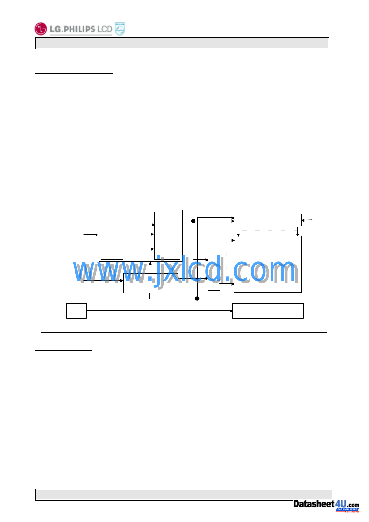
RGB(O)
Power
Block
Timing
Control
Block
Row Driver circuit
RGB(E)
FlatLink
CN1
www.jxlcd.com
www.jxlcd.com
CN2
Clock
(THC63LVD 824)
General Features
Active screen size 14.1 inches(35.7cm) diagonal
Outline dimensions 298.5(H) × 227.0(V) mm (Typ.), 6.0(D) mm(Max.)
Pixel pitch 0.204 mm × 0.204 mm
Pixel format 1400 horiz. by 1050 vert. pixels
RGB stripe arrangement
Color depth 6-bit, 262,144 colors
Luminance,White 185 cd/m2 (Typ.)
Power Consumption 1.32W typ. (Circuit) / 4.08W Max. (Backlight)
Weight 510g (Typ.)
Display operating mode Transmissive mode, normally white
Surface treatments Hard coating (3H),
Anti-glare treatment of the front polarizer
Column driver circuit
TFT -LCD
(1400×1050)
Backlight Ass’y
Ver 1.4 NOV 10, 2000 Page 1 /8

Display
Product Specification
LP141E2
Liquid Crystal
2. Electrical Specifications
2-1. Electrical Characteristics
The LP141E2-A1 requires two power inputs. One is employed to power the LCD electronics and to drive the
TFT array and liquid crystal. The second input which powers the CCFL, is typically generated by an inverter.
The inverter is an external unit to the LCD.
Table 1 ELECTRICAL CHARACTERISTICS:
Parameter Symbol Values Units Notes
Min. Typ. Max.
MODULE:
Power Supply Input Voltage
Power Supply Input Current
Differential Impedance
Power Consumption
Rush current (I2t)
LAMP
Operating Voltage
Operating Current
Established Starting Voltage
at 25 °C
at 0 °C
Operating Frequency
Discharge Stabilization time
Power Consumption
Life Time(at 25 °C)
Notes: 1. The specified current and power consumption are under the Vcc = 3.3V , 25 °C, fv = 50Hz condition
whereas Black pattern is displayed.
3. Littel Fuse guarantees 100,000 pulses(Inrush current), If I2t is less than 22%.
4. The variance of the voltage is +- 10%.
horizontal synchronous frequency and from its harmonics in order to prevent interference.
Ts is the time required for the brightness of the center of the lamp to be not less than 95%.
8.The lamp power consumption shown above does not include loss of external inverter.
9. The life time is determined as the time at which brightness of lamp is 50% compare to that of initial
www.jxlcd.com
www.jxlcd.com
2. This impedance value is needed to proper display and measured form LVDS Tx to the mating
connector.
5. The transformer output voltage in the inverter must be high considering to the loss of the ballast
capacitor in the inverter.
The voltage above Vs should be applied to the lamps for more than 1second for start -up.
Otherwise, the lamps may not be turned on.
6. The output of the inverter must have symmetrical(negative and positive) voltage waveform and
symmetrical current waveform.(Unsymmetrical ratio is less than 10%) Please do not use the inverter
which has unsymmetrical voltage and unsymmetrical current and spike wave.
Lamp frequency may produce interference with horizontal synchronous frequency and as a result
this may cause beat on the display. Therefore lamp frequency shall be as away as possible from the
7.Let’s define the brightness of the lamp after being lighted for 5 minutes as 100%.
value at the typical lamp current on condition of continuous operating at 25 +- 2°C .
V
CC
I
CC
Zm
Pc
V
IBL
f
BL
TS
PBL
BL
3.0
-
90
-
-
680
3.0
-
-
45
-
10,000
3.3
0.400
100
1.32
-
725
5.0
-
-
60
3.63
15,000
3.6
0.450
110
1.50
10
850
6.0
1100
1450
80
3
4.08
-
Vdc
A
ohm
Watts
%
V
RMS
mA
V
RMS
V
RMS
KHz
Minutes
Watts
Hrs
1
2
1
3
4
5
6
7
8
9
Ver 1.4 NOV 10, 2000 Page 2 /8
Display
No. 1
30
Product Specification
LP141E2
Liquid Crystal
2-2. Interface Connections
This LCD employs two interface connections, a 30 pin connector is used for the module electronics and the
other connector is used for the integral backlight system.
The electronics interface connector is a model FI-XB30SR-HF11 manufactured by JAE or equivalent. The pin
configuration for the connector is shown in the table below.
Pin Symbol Description Notes
1
2
3
4
5
6
7
8
9
10
11
12
13
14
15
16
17
18
19
20
21
22
23
24
25
26
27
28
29
30
RCLK1-
RCLK1+
RCLK1-
RCLK2+
Table 2 MODULE CONNECTOR PIN CONFIGURATION (LVDS) [CN1]
Mode
Vcc
Vcc
GND
GND
NC
NC
RA1-
RA1+
GND
RB1-
RB1+
GND
RC1-
RC1+
www.jxlcd.com
www.jxlcd.com
GND
GND
RA2-
RA2+
GND
RB2-
RB2+
GND
RC2-
RC2+
GND
Supply Voltage(+3.3V)
Supply Voltage(+3.3V)
No Connection
No Connection
Odd Channel Differential signal
Odd Channel Differential signal
Odd Channel Differential signal
Odd Channel Differential signal
Odd Channel Differential signal
Odd Channel Differential signal
Odd Channel Differential signal
Odd Channel Differential signal
Even Channel Differential signal
Even Channel Differential signal
Even Channel Differential signal
Even Channel Differential signal
Even Channel Differential signal
Even Channel Differential signal
Even Channel Differential signal
Even Channel Differential signal
Option
Ground
Ground
Ground
Ground
Ground
Ground
Ground
Ground
Ground
1. Interface chips
1.1 LCD : LPZ4E122S6L (Thine)
(THC63LVDF824A core + Timing Controller)
1.2 System : THC63LVDM8233A (Thine)
2. Mode option
-. High : 1-channel(Odd channel)
-. Low : 2- channel(Odd, Even channel)
3. Connector
2.1 LCD : FI-XB30SR -HF11 (JAE)
or compatible
2.2 Mating
-. Wire type : FI-X30H (JAE)
-. FPC type : FI-X30M (JAE)
2.3 Connector pin arrangement
···
CN1
Viewing on Display side
CN2
Ver 1.4 NOV 10, 2000 Page 3 /8
 Loading...