

LG LP-133WX3-TLA4 Service manual
( ) Preliminary Specification
◆
( ) Final Specification
Title 13.3” WXGA TFT LCD
LP133WX3
Liquid Crystal Display
Product Specification
SPECIFICATION
FOR
APPROVAL
Customer APPLE
MODEL K6
www.jxlcd.com
www.jxlcd.com
APPROVED BY SIGNATURE
/
/
/
SUPPLIER LG. Display Co., Ltd.
*MODEL LP133WX3
Suffix TLA4
*When you obtain standard approval,
please use the above model name without suffix
APPROVED BY SIGNATURE
J.K.Kim/ S.Manager
REVIEWED BY
K.T.Moon/ Manager
PREPARED BY
H. H. Lee / Engineer
Please return 1 copy for your confirmation with
your signature and comments.
Ver. 0.0 Oct.23, 2009
Product Engineering Dept.
LG. Display Co., Ltd
1 / 27
Product Specification
Contents
LP133WX3
Liquid Crystal Display
No ITEM
COVER
CONTENTS
RECORD OF REVISIONS
1 GENERAL DESCRIPTION
2 ABSOLUTE MAXIMUM RATINGS
3 ELECTRICAL SPECIFICATIONS
3-1 ELECTRICAL CHARACTREISTICS
3-2 INTERFACE CONNECTIONS
3-3 LVDS SIGNAL TIMING SPECIFICATIONS
3-4 SIGNAL TIMING WAVEFORMS
3-5 COLOR INPUT DATA REFERNECE
www.jxlcd.com
www.jxlcd.com
3-6 POWER SEQUENCE
4 OPTICAL SFECIFICATIONS
5 MECHANICAL CHARACTERISTICS
Page
1
2
3
4
5
6
7
8
11
12
13
14
18
6 RELIABLITY
7 INTERNATIONAL STANDARDS
7-1 SAFETY
7-2 EMC
8 PACKING
8-1 DESIGNATION OF LOT MARK
8-2 PACKING FORM
9 PRECAUTIONS
A APPENDIX. Enhanced Extended Display Identification Data
Ver. 0.0 Oct.23, 2009
21
22
22
23
23
24
26
2 / 27
Product Specification
RECORD OF REVISIONS
LP133WX3
Liquid Crystal Display
Revision No Revision Date Page Description
0.0 23. Oct. 2009 - First Draft 0.0
www.jxlcd.com
www.jxlcd.com
EDID
ver
Ver. 0.0 Oct.23, 2009
3 / 27
LP133WX3
Liquid Crystal Display
Product Specification
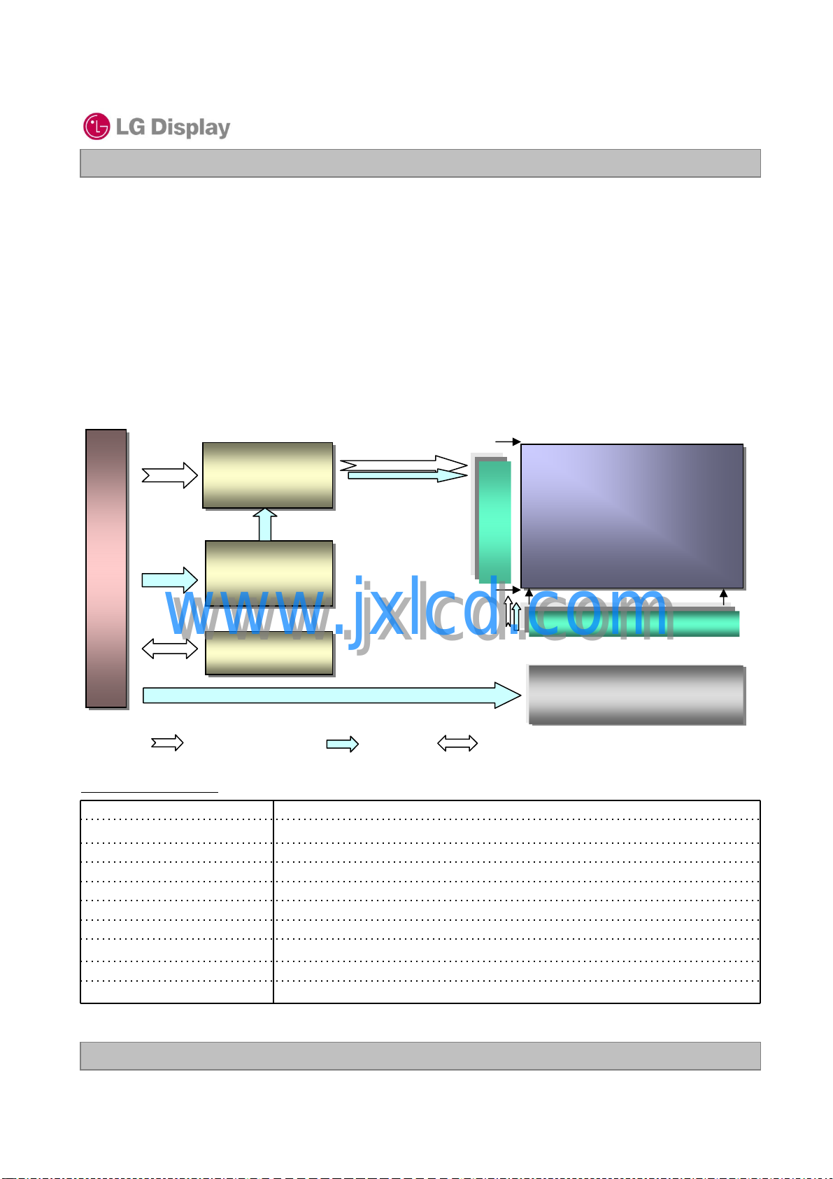
1. General Description
The LP133WX3 is a Color Active Matrix Liquid Crystal Display with an integral LED backlight system. The
matrix employs a-Si Thin Film Transistor as the active element. It is a transmissive type display operating in
the normally white mode. This TFT-LCD has 13.3 inches diagonally measured active display area with WXGA
resolution(1280 horizontal by 800 vertical pixel array). Each pixel is divided into Red, Green and Blue subpixels or dots which are arranged in vertical stripes. Gray scale or the brightness of the sub-pixel color is
determined with a 6-bit gray scale signal for each dot, thus, presenting a palette of more than 262,144 colors.
The LP133WX3 has been designed to apply the interface method that enables low power, high speed, low
EMI.
The LP133WX3 is intended to support applications where thin thickness, low power are critical factors and
graphic displays are important. In combination with the vertical arrangement of the sub-pixels, the LP133WX3
characteristics provide an excellent flat display for office automation products such as Notebook PC.
800
1
Gate Driver
TFT-LCD Panel
(1280 x 800)
(LOG_B type)
(LOG_B type)
(LOG_B type)(LOG_B type)
1
Source Driver Circuit
LED Backlight Ass’y
9LEDs X 6 strings
CN
User connector
30
Pin
LVDS &
Timing
1
www.jxlcd.com
www.jxlcd.com
Control & Data Power EDID signal & Power
Control
Block
POWER
BLOCK
EDID
BLOCK
General Features
Active Screen Size 13.3 inches diagonal
Outline Dimension 297.15 (H) × 192.15 (V) ×
Pixel Pitch 0.2235 mm × 0.2235 mm
Pixel Format 1280 horiz. by 800 vert. Pixels RGB strip arrangement
Color Depth 6-bit, 262,144 colors
Luminance, White 275cd/m2(Typ., @I
Power Consumption Logic : 0.76W(typ.@Mosaic), Back Light : 3.4W(typ.@ I
Weight
Display Operating Mode Transmissive mode, normally white
Surface Treatment Hard Coating(Glare), Anti reflection treatment of the front Polarizer (Haze 0%)
310(Max.)
LED
3.75(D, Max.) mm
=20mA)
= 21mA)
LED
1280
Ver. 0.0 Oct.23, 2009
4 / 27
LP133WX3
Liquid Crystal Display
Product Specification
2. Absolute Maximum Ratings
The following are maximum values which, if exceeded, may cause faulty operation or damage to the unit.
Table 1. ABSOLUTE MAXIMUM RATINGS
Parameter Symbol
Power Input Voltage
Operating Temperature
Storage Temperature
Operating Ambient Humidity
Storage Humidity
Note : 1. Temperature and relative humidity range are shown in the figure below.
Wet bulb temperature should be 39°C Max, and no condensation of water.
www.jxlcd.com
www.jxlcd.com
Wet Bulb
Temperature [℃℃℃℃]
20
10
0
VCC -0.3 4.0 Vdc at 25 ± 5°C
TOP 0 50 °C 1
HST -20 60 °C 1
HOP 10 90 %RH 1
HST 10 90 %RH 1
50
40
30
Values
Min Max
90% 80%
60
Units Notes
60%
Humidity[(%)RH]
Storage
40%
Operation
20%
10%
-20
Ver. 0.0 Oct.23, 2009
10
20 30 40 50
Dry Bulb Temperature [℃℃℃℃]
60 70 800
5 / 27
LP133WX3
Liquid Crystal Display
Product Specification
3. Electrical Specifications
3-1. Electrical Characteristics
The LP133WX3 requires two power inputs. One is employed to power the LCD electronics and to drive the
TFT array and liquid crystal. The second input which powers the LED BL.
Table 2. ELECTRICAL CHARACTERISTICS
Parameter Symbol
MODULE :
Power Supply Input Voltage VCC 3.0 3.3 3.6 V
Power Supply Input Current I
Power Consumption Pc - 0.76 0.875 Watt 1
Differential Impedance Zm 90 100 110 Ohm 2
LED Backlight :
Operating Current per string I
Power Consumption P
Life Time 10,000 - - Hrs 5
CC
Mosaic - 230 265 mA 1
LED
BL
Min Typ Max
5 20 21 mA 3
- 3.46 - Watt 4
Values
Unit Notes
DC
www.jxlcd.com
www.jxlcd.com
Note)
1. The specified current and power consumption are under the Vcc = 3.3V , 25℃, fv = 60.2Hz condition
whereas Mosaic pattern is displayed and fv is the frame frequency.
2. This impedance value is needed to proper display and measured form LVDS Tx to the mating connector.
3. The typical operating current is for the typical surface luminance (LWH) in optical characteristics.
4. The LED power consumption shown above does not include power of external LED driver circuit
for typical current condition.
5. The life time is determined as the time at which brightness of lamp is 50% compare to that of initial value
at the typical lamp current.
Ver. 0.0 Oct.23, 2009
6 / 27

LP133WX3
Liquid Crystal Display
Product Specification
3-2. Interface Connections
This LCD employs two interface connections, a 30 pin connector is used for the module electronics interface
and the other connector is used for the integral backlight system.
The electronics interface connector is a model 20474-030E-12 manufactured by I-PEX.
Table 3. MODULE CONNECTOR PIN CONFIGURATION (CN1)
Pin Symbol Description Notes
1 GND Ground [LVDS Receiver]
2 VCC Power Supply, 3.3V Typ.
3 VCC Power Supply, 3.3V Typ.
4 V EEDID DDC 3.3V power
5 GSP
6 Clk EEDID DDC Clock
7 DATA EEDID DDC Data
8 RIN0- Negative LVDS differential data input
9 RIN0+ Positive LVDS differential data input
10 GND Ground
11 RIN1- Negative LVDS differential data input
12 RIN1+ Positive LVDS differential data input
13 GND Ground
14 RIN2- Negative LVDS differential data input
15 RIN2+ Positive LVDS differential data input
16 GND Ground
17 CLKIN- Negative LVDS differential clock input
18 CLKIN+ Positive LVDS differential clock input
19 GND Ground
20 NC
21 Vdc LED Anode (Positive)
22 Vdc LED Anode (Positive)
23 NC
24 Vdc1 LED Cathode (Negative)
25 Vdc2 LED Cathode (Negative)
26 Vdc3 LED Cathode (Negative)
27 Vdc4 LED Cathode (Negative)
28 Vdc5 LED Cathode (Negative)
29 Vdc6 LED Cathode (Negative)
30 NC
www.jxlcd.com
www.jxlcd.com
GSP
No Connection
No Connection
No Connection
[LVDS Receiver]
[LVDS Receiver][LVDS Receiver]
SiliconWorks, SW0618V
[Connector]
[Connector]
[Connector][Connector]
I-PEX 20474-030E–1#
[Mating Connector]
[Mating Connector]
[Mating Connector][Mating Connector]
I-PEX 20472-030T-10 series
or equivalent (micro-coax type)
[Connector pin arrangement]
[Connector pin arrangement]
[Connector pin arrangement][Connector pin arrangement]
LCD front view
1
3
0
Ver. 0.0 Oct.23, 2009
7 / 27
Product Specification
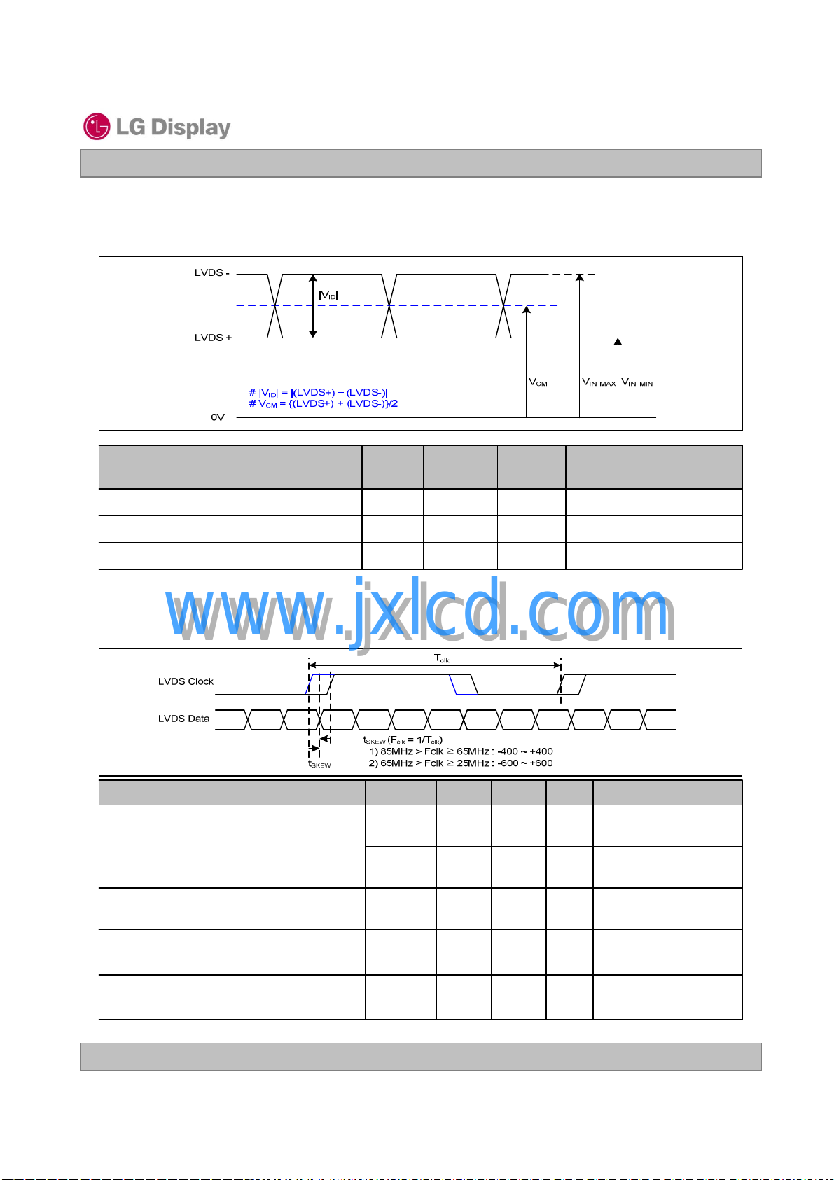
3-3. LVDS Signal Timing Specifications
3-3-1. DC Specification
LP133WX3
Liquid Crystal Display
Description
LVDS Differential Voltage |VID| 100 600 mV -
LVDS Common mode Voltage V
LVDS Input Voltage Range V
3-3-2. AC Specification
LVDS Clock to Data Skew Margin
www.jxlcd.com
www.jxlcd.com
Description Symbol Min Max Unit Notes
Symb
ol
CM
IN
t
SKEW
t
SKEW
Min Max Unit Notes
0.6 1.8 V -
0.3 2.1 V -
- 400 + 400 ps
- 600 + 600 ps
85MHz > Fclk ≥
65MHz > Fclk ≥
65MHz
25MHz
LVDS Clock to Clock Skew Margin (Even
to Odd)
Maximum deviation
of input clock frequency during SSC
Maximum modulation frequency
of input clock during SSC
Ver. 0.0 Oct.23, 2009
t
SKEW_EO
F
DEV
F
MOD
- 1/7 + 1/7 T
- ± 3 % -
- 200 KHz -
clk
-
8 / 27
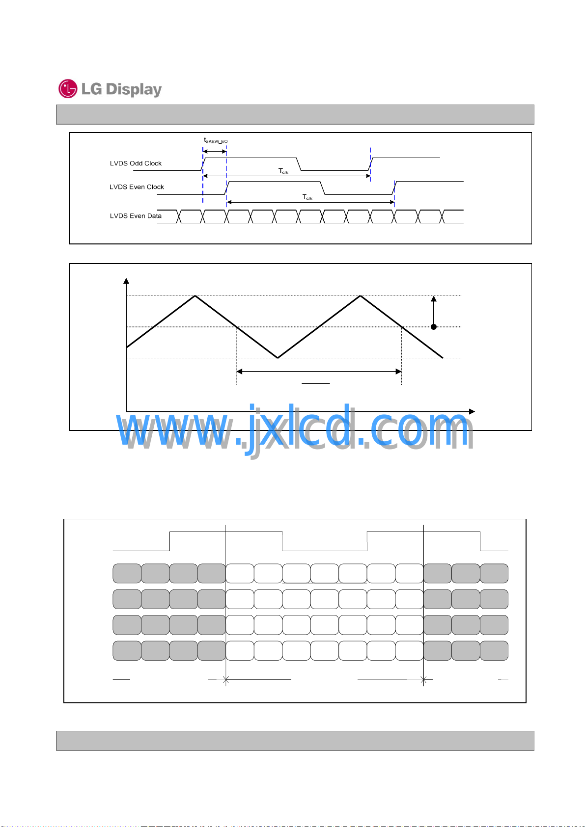
Freq.
F
max
F
center
F
min
Product Specification
< Clock skew margin between channel >
LP133WX3
Liquid Crystal Display
F
* F
center
DEV
www.jxlcd.com
www.jxlcd.com
3-3-3. Data Format
1) LVDS 1 Port
RCLK+
RA+/-
RB+/-
RC+/-
RD+/-
R3 R2
G4 G3
B5 B4
G7 G6
R1 R0
G2 G1
B3 B2
R7 R6
1
F
MOD
< Spread Spectrum >
G0 R5 R4 R3 R2 R1 R0
B1 B0 G5 G4 G3 G2 G1
DE VSYNC HSYNC B5 B4 B3 B2
X B7 B6 G7 G6 R7 R6
G0
B1
DE
VSYNC HSYNC
X
Time
R5 R4
B0 G5
B7 B6
Previous (N-1)th Cycle Next (N+1)th Cycle
< LVDS Data Format >
Ver. 0.0 Oct.23, 2009
Current (Nth ) Cycle
9 / 27
 Loading...