

LG LP-121WX3-TLA1 Service manual
Product Specification
LP121WX3
Liquid Crystal Display
www.jxlcd.com
www.jxlcd.com
Ver. 1.0 Dec. 10, 2008
0 / 30
( )Preliminary Specification
( )Final Specification
◆
Title 12.1” WXGA TFT LCD
LP121WX3
Liquid Crystal Display
Product Specification
SPECIFICATION
FOR
APPROVAL
Customer HP
MODEL
www.jxlcd.com
www.jxlcd.com
APPROVED BY SIGNATURE
/
/
/
SUPPLIER LG Display Co., Ltd.
*MODEL LP121WX3
Suffix TLA1
*When you obtain standard approval,
please use the above model name without suffix
APPROVED BY
G. J. Kwon / G.Manager
REVIEWED BY
W. Y. Park / Manager
PREPARED BY
S. Y. Kim / Engineer
T.S. Yun / Engineer
SIGNATURE
Please return 1 copy for your confirmation with
your signature and comments.
Ver. 1.0 Dec. 10, 2008
Products Engineering Dept.
LG Display Co., Ltd
1 / 30

Product Specification
Contents
LP121WX3
Liquid Crystal Display
No ITEM
COVER
CONTENTS
RECORD OF REVISIONS
1 GENERAL DESCRIPTION
2 ABSOLUTE MAXIMUM RATINGS
3 ELECTRICAL SPECIFICATIONS
3-1 ELECTRICAL CHARACTREISTICS
3-2 INTERFACE CONNECTIONS
3-3 LVDS SIGNAL TIMING SPECIFICATIONS
3-4 SIGNAL TIMING SPECIFICATIONS
3-5 SIGNAL TIMING WAVEFORMS
www.jxlcd.com
www.jxlcd.com
3-6 COLOR INPUT DATA REFERNECE
3-7 POWER SEQUENCE
4 OPTICAL SFECIFICATIONS
Page
1
2
3
4
5
6
8
9
11
11
12
13
14
5 MECHANICAL CHARACTERISTICS
6 RELIABLITY
7 INTERNATIONAL STANDARDS
7-1 SAFETY
7-2 EMC
8 PACKING
8-1 DESIGNATION OF LOT MARK
8-2 PACKING FORM
9 PRECAUTIONS
A APPENDIX. Enhanced Extended Display Identification Data
Ver. 1.0 Dec. 10, 2008
17
24
25
25
26
26
27
29
2 / 30
Product Specification
RECORD OF REVISIONS
LP121WX3
Liquid Crystal Display
Revision No Revision Date Page Description
0.0 May 21. 2008 - First Draft (Preliminary Specification) 0.0
0.1 Sep. 05. 2008 28~30 Update of the EEDID Table
6 Update of the Electrical characteristics.
0.2 Oct. 23. 2008
1.0 Dec. 10. 2008 - Final Specification 1.0
www.jxlcd.com
www.jxlcd.com
13~14 Update of the optical characteristics.
16~17 Change of the mechanical drawing.
6 Update the Electrical characteristics.
12 Update the Power Sequence.
EDID
ver
Ver. 1.0 Dec. 10, 2008
3 / 30
LP121WX3
Liquid Crystal Display
Product Specification
1. General Description
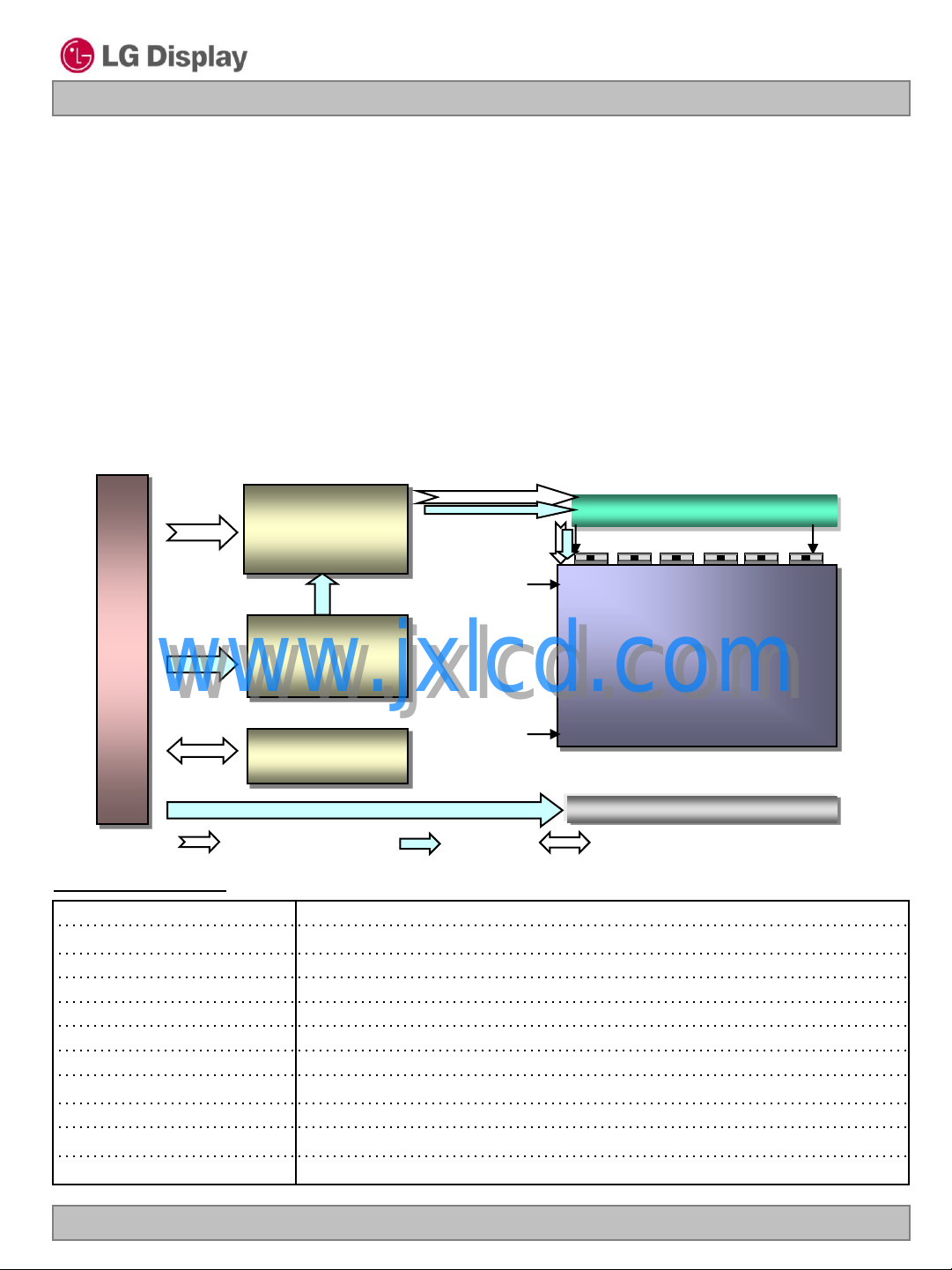
The LP121WX3 is a Color Active Matrix Liquid Crystal Display with an integral White LED backlight system.
The matrix employs a-Si Thin Film Transistor as the active element. It is a transmissive type display
operating in the normally white mode. This TFT-LCD has 12.1 inches diagonally measured active display
area with WXGA resolution(800 vertical by 1280 horizontal pixel array). Each pixel is divided into Red,
Green and Blue sub-pixels or dots which are arranged in vertical stripes. Gray scale or the brightness of the
sub-pixel color is determined with a 6-bit gray scale signal for each dot, thus, presenting a palette of more
than 262,144 colors.
The LP121WX3 has been designed to apply the interface method that enables low power, high speed, low
EMI.
The LP121WX3 is intended to support applications where thin thickness, low power are critical factors and
graphic displays are important. In combination with the vertical arrangement of the sub-pixels, the
LP121WX3 characteristics provide an excellent flat display for office automation products such as Notebook
PC.
LVDS &
CN
1
User connector
www.jxlcd.com
www.jxlcd.com
40
Pin
Control & Data Power EDID signal & Power
Timing
Control
Block
POWER
BLOCK
EDID
BLOCK
1
GIP(Gate In Panel)
800
Source Driver Circuit
1
TFT-LCD Panel
(1280 x 800)
Backlight Ass’y
General Features
Active Screen Size 12.1 inches diagonal
Outline Dimension
Pixel Pitch
Pixel Format 1280 horiz. By 800 vert. Pixels RGB strip arrangement
Color Depth 6-bit, 262,144 colors
Luminance, White 200 cd/m2(Typ.5 point)
Power Consumption Total 4.0 Watt(Typ.) @ LCM circuit 0.8Watt(Typ.), B/L input 3.2Watt(Typ.)
Weight 270g(Max.)
Display Operating Mode Transmissive mode, normally white
Surface Treatment Glare treatment of the front polarizer
RoHS Comply Yes
275.8 (H) × 178.1 (V) × 5.5(D, max) mm
0.204 mm × 0.204 mm
1280
Ver. 1.0 Dec. 10, 2008
4 / 30
LP121WX3
Liquid Crystal Display
Product Specification
2. Absolute Maximum Ratings
The following are maximum values which, if exceeded, may cause faulty operation or damage to the unit.
Table 1. ABSOLUTE MAXIMUM RATINGS
Parameter Symbol
Power Input Voltage
Operating Temperature
Storage Temperature
Operating Ambient Humidity
Storage Humidity
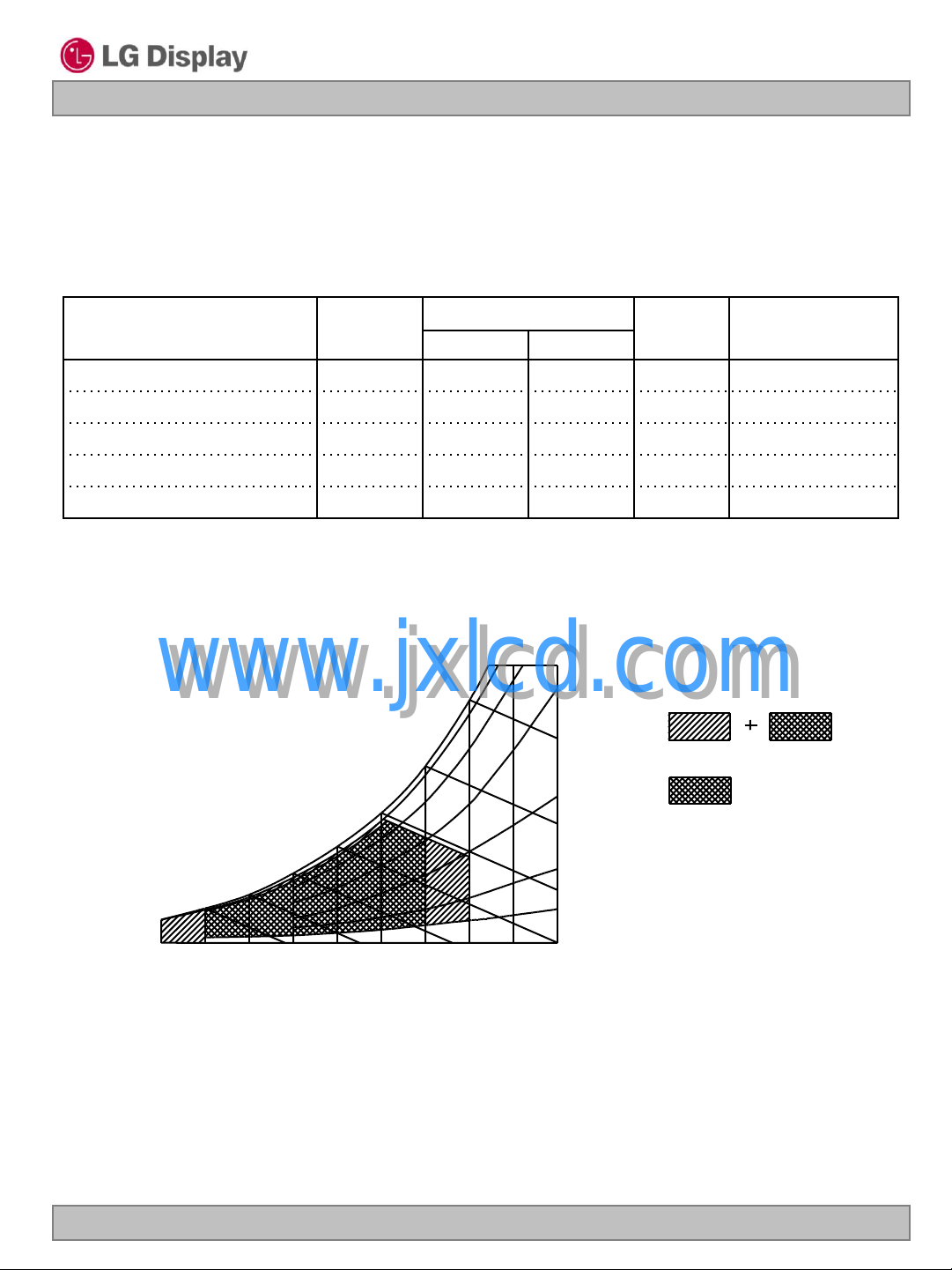
Note : 1. Temperature and relative humidity range are shown in the figure below.
Wet bulb temperature should be 39C Max, and no condensation of water.
www.jxlcd.com
www.jxlcd.com
Wet Bulb
Temperature[℃]
20
10
0
VCC -0.3 4.0 Vdc
TOP 0 50
HST -20 60
HOP 10 90 %RH 1
HST 10 90 %RH 1
50
40
30
Values
Min Max
90% 80%
60
Units Notes
C
C
60%
Humidity[(%)RH]
Storage
40%
Operation
20%
10%
at 25 5C
1
1
-20
Ver. 1.0 Dec. 10, 2008
10
20 30 40 50
Dry Bulb Temperature [℃]
60 70 800
5 / 30
LP121WX3
Liquid Crystal Display
Product Specification
3. Electrical Specifications
3-1. Electrical Characteristics
The LP121WX3 requires two power inputs. The first logic is employed to power the LCD electronics and to
drive the TFT array and liquid crystal. The second backlight is the input about LED BL.with LED Driver.
Table 2. ELECTRICAL CHARACTERISTICS
Parameter Symbol
MODULE :
Power Supply Input Voltage VCC 3.0 3.3 3.6 V
Power Supply Input Current I
Power Consumption Pc Mosaic - 0.8 0.9 W
LVDS Impedance ZLVDS 90 100 110 Ω 2
LED Backlight:
Operating Current per string I
Operating Voltage per string V
Power Consumption P
Life Time 12,000 Hrs 4
LED Driver
Power Supply Input Voltage V
Frequency F
PWM Dimming (Duty) Ratio D
PWM High Voltage Level V
PWM Low Voltage Level V
LED_EN High Voltage V
LED_EN Low Voltage V
Note)
1. The specified current and power consumption are under the Vcc = 3.3V , 25℃, fv= 60Hz condition
whereas Mosaic pattern is displayed and fv is the frame frequency.
www.jxlcd.com
www.jxlcd.com
CC
Mosaic - 250 280 mA 1
LED
LED
BL
BL+
PWM
on
PWM_H
PWM_L
LED_EN_H
LED_EN_L
Min Typ Max
5.0 20.0 21.0 mA 3
- 22.1 23.8 V
7.0 12.0 20.0 V
200 1000 Hz 5
12.5 - 100 % 6
3.0 - 5.3 V
0 - 0.5 V
3.0 - 5.3 V
0 - 0.5 V
Values
3.1 3.4 W 3
Unit Notes
DC
2. This impedance value is needed to proper display and measured form
LVDS Tx to the mating connector.
3. The specified LED current and power consumption are under the Vled = 12.0V , 25℃, Dimming of Max
luminance whereas White pattern is displayed and fv is the frame frequency.
4. The life time is determined as the time at which brightness of LCD is 50% compare to that of initial value
at the typical LED current. These LED backlight has 6 strings on it and the typical current of LED‟s string
is base on 20mA
5. This Spec. is not effective at 100% dimming ratio as an exception because it has DC level equivalent
to 0Hz. In spite of acceptable range as defined, the PWM Frequency should be fixed and stable for
more consistent brightness control at any specific level desired.
6. The operation of LED Driver below minimum dimming ratio may cause flickering or reliability issue.
Ver. 1.0 Dec. 10, 2008
6 / 30
LP121WX3
Liquid Crystal Display
Product Specification
3-2. Interface Connections
This LCD employs one interface connections, a 40 pin connector is used for the module electronics interface
and the integral backlight system.
The electronics interface connector is a model FI-NXB40SL-HF10 manufactured by JAE.
Table 3. MODULE CONNECTOR PIN CONFIGURATION (CN1)
Pin Symbol Description Notes
1 NC No Connection (Reserved for supplier)
2 VCC Power Supply, 3.3V (typical)
3 VCC Power Supply, 3.3V (typical)
4 V EEDID DDC 3.3V power
5 NC No Connection
6 Clk EEDID DDC Clock
7 DATA EEDID DDC Data
8
9
10
11
12
13
14
15
16
17
18
19 GND Ground
20 NC No Connection
21 NC No Connection
22 GND Ground
23 NC No Connection
24 NC No Connection
25 GND Ground
26 NC No Connection
27 NC No Connection
28 GND Ground
29 NC No Connection
30 NC No Connection
31 VBL- LED Ground
32 VBL- LED Ground
33 VBL- LED Ground
34 NC No Connection (Reserved for supplier)
35 VBL+ LED Power Supply 6V-20V
36 VBL+ LED Power Supply 6V-20V
37 VBL+ LED Power Supply 6V-20V
38 BLIM PWM for luminance control (200Hz ~ 1000Hz)
39 BL_Enable Backlight On/Off Control
40 NC No Connection (Reserved for supplier)
RIN0- Negative LVDS differential data input
RIN0+ Positive LVDS differential data input
GND Ground
RIN1- Negative LVDS differential data input
RIN1+ Positive LVDS differential data input
GND Ground
RIN2- Negative LVDS differential data input
RIN2+ Positive LVDS differential data input
GND Ground
CLKIN- Negative LVDS differential clock input
www.jxlcd.com
CLKIN+ Positive LVDS differential clock input
www.jxlcd.com
1, Interface chips
1.1 LCD : SW, SW0612B (LCD Controller)
including LVDS Receiver
1.2 System : THC63LVD823A or equivalent
* Pin to Pin compatible with LVDS
2. Connector
2.1 LCD : FI-NXB40SL-HF10, JAE
2.2 Mating : FI-NX400L or equivalent.
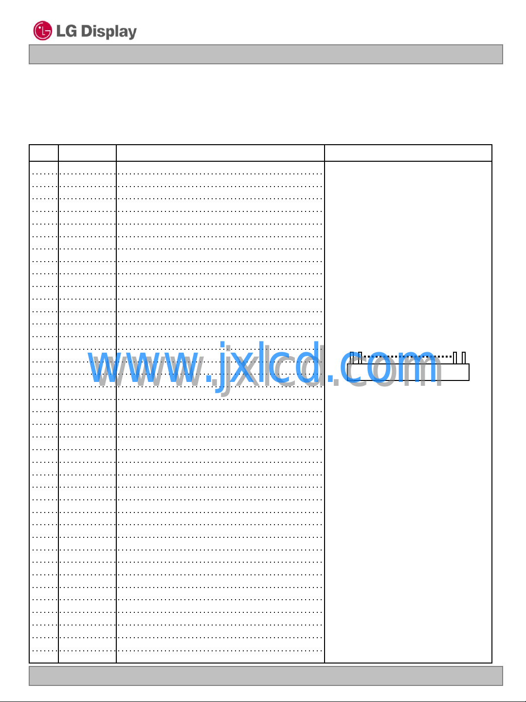
2.3 Connector pin arrangement
40
it‟s compatible.
1
[LCD Module Rear View]
Ver. 1.0 Dec. 10, 2008
7 / 30
Product Specification
LVDS +
LVDS -
0V
V
CM
# |VID| = |(LVDS+) – (LVDS-)|
# VCM = {(LVDS+) + (LVDS-)}/2
|VID|
V
IN_MAXVIN_MIN
LVDS Data
t
SKEW
LVDS Clock
T
clk
t
SKEW (Fclk
= 1/T
clk
)
1) 85MHz > Fclk ≥ 65MHz : -400 ~ +400
2) 65MHz > Fclk ≥ 25MHz : -600 ~ +600
3-3. LVDS Signal Timing Specifications
3-3-1. DC Specification
LP121WX3
Liquid Crystal Display
Description
Symb
ol
Min Max Unit Notes
LVDS Differential Voltage |VID| 100 600 mV LVDS Common mode Voltage V
LVDS Input Voltage Range V
3-3-2. AC Specification
www.jxlcd.com
www.jxlcd.com
CM
IN
0.6 1.8 V -
0.3 2.1 V -
Description Symbol Min Max Unit Notes
t
SKEW
- 400 + 400 ps
85MHz > Fclk ≥
LVDS Clock to Data Skew Margin
t
SKEW
- 600 + 600 ps
65MHz > Fclk ≥
65MHz
25MHz
LVDS Clock to Clock Skew Margin (Even
to Odd)
Maximum deviation
of input clock frequency during SSC
Maximum modulation frequency
of input clock during SSC
Ver. 1.0 Dec. 10, 2008
t
SKEW_EO
F
DEV
F
MOD
- 1/7 + 1/7 T
clk
- ± 3 % -
- 200 KHz -
-
8 / 30
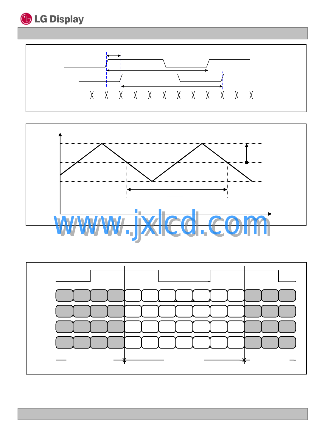
LVDS Even Data
LVDS Odd Clock
LVDS Even Clock
t
SKEW_EO
T
clk
T
clk
Freq.
F
max
F
center
F
min
Product Specification
< Clock skew margin between channel >
LP121WX3
Liquid Crystal Display
F
* F
center
DEV
www.jxlcd.com
www.jxlcd.com
3-3-3. Data Format
1) LVDS 1 Port
RCLK+
RA+/-
RB+/-
RC+/-
RD+/-
R3 R2
G4 G3
B5 B4
G7 G6
Previous (N-1)th Cycle Next(N+1)th Cycle
R1 R0
G2 G1
B3 B2
R7 R6
1
F
MOD
< Spread Spectrum >
G0 R5 R4 R3 R2 R1 R0
B1 B0 G5 G4 G3 G2 G1
DE VSYNC HSYNC B5 B4 B3 B2
X B7 B6 G7 G6 R7 R6
Current (Nth) Cycle
Time
G0
B1
DE
VSYNC HSYNC
X
R5 R4
B0 G5
B7 B6
Ver. 1.0 Dec. 10, 2008
< LVDS Data Format >
9 / 30
 Loading...