

LG LP-116WH2-TLC1 Service manual

LP116WH2
www.DataSheet.net/
Datasheet pdf - http://www.DataSheet4U.co.kr/
Liquid Crystal Display
Product Specification
SPECIFICATION
FOR
APPROVAL
)
(
(
Preliminary Specification
)
Final Specification
◆
11.6” HD TFT LCDTitle
DellCustomer
MODEL
*When you obtain standard approval,
www.jxlcd.com
www.jxlcd.com
SIGNATUREAPPROVED BY
/
/
/
please use the above model name without suffix
APPROVED BY
C. J. Jun / Manager
REVIEWED BY
S. W. Paeng / Manager
PREPARED BY
P. A. Choi / Engineer
LG Display Co., Ltd.SUPPLIER
LP116WH2*MODEL
TLC1Suffix
SIGNATURE
Please return 1 copy for your confirmation with
your signature and comments.
Ver. 1.0 Aug. 18, 2009
Products Engineering Dept.
LG Display Co., Ltd
1 / 27
Product Specification
www.DataSheet.net/
Datasheet pdf - http://www.DataSheet4U.co.kr/
Contents
LP116WH2
Liquid Crystal Display
ITEMNo
COVER
CONTENTS
RECORD OF REVISIONS
GENERAL DESCRIPTION1
ABSOLUTE MAXIMUM RATINGS2
ELECTRICAL SPECIFICATIONS3
ELECTRICAL CHARACTREISTICS3-1
INTERFACE CONNECTION3-2
LVDS SIGNAL TIMING SPECIFICATIONS3-3
SIGNAL TIMING SPECIFICATIONS3-4
SIGNAL TIMING WAVEFORMS3-5
www.jxlcd.com
www.jxlcd.com
COLOR INPUT DATA REFERNECE3-6
POWER SEQUENCE3-7
OPTICAL SFECIFICATIONS4
Page
1
2
3
4
5
6
7
8
10
10
11
12
13
MECHANICAL CHARACTERISTICS5
RELIABLITY6
INTERNATIONAL STANDARDS7
SAFETY7-1
EMC7-2
PACKING8
DESIGNATION OF LOT MARK8-1
PACKING FORM8-2
PRECAUTIONS9
APPENDIX. Enhanced Extended Display Identification Data A
Ver. 1.0 Aug. 18, 2009
16
20
21
21
22
22
23
25
2 / 27
Product Specification
www.DataSheet.net/
Datasheet pdf - http://www.DataSheet4U.co.kr/
RECORD OF REVISIONS
LP116WH2
Liquid Crystal Display
DescriptionPageRevision DateRevision No
First Draft (Preliminary Specification)AllApr. 02. 20090.0
Label Information Add19
Packing Form update22
Power Consumption, PWM Frequency, PWM Duty ranges are6
limited.
Dclk Typ. is changed to 71.1 as real Dclk.10
Color Coordinates is confirmed.13
14
Gray scale specification is confirmed.
Final EDID25-27
www.jxlcd.com
www.jxlcd.com
EDID
ver
-
-Mechanical Dimension(Mount Hole shape change)17Jun. 02. 20090.1
-Final CASAug.18.20091.0
Ver. 1.0 Aug. 18, 2009
3 / 27
LP116WH2
www.DataSheet.net/
Datasheet pdf - http://www.DataSheet4U.co.kr/
Liquid Crystal Display
Product Specification
1. General Description
The LP116WH2 is a Color Active Matrix Liquid Crystal Display with an integral LED backlight system. The
matrix employs a-Si Thin Film Transistor as the active element. It is a transmissive type display operating in
the normally white mode. This TFT-LCD has 10.1inches diagonally measured active display area with HD
resolution(1366 horizontal by 768 vertical pixel array). Each pixel is divided into Red, Green and Blue subpixels or dots which are arranged in vertical stripes. Gray scale or the brightness of the sub-pixel color is
determined with a 6-bit gray scale signal for each dot, thus, presenting a palette of more than 262,144
colors.
The LP116WH2 has been designed to apply the interface method that enables low power, high speed, low
EMI.
The LP116WH2 is intended to support applications where thin thickness, low power are critical factors and
graphic displays are important. In combination with the vertical arrangement of the sub-pixels, the
LP116WH2 characteristics provide an excellent flat display for office automation products such as Notebook
PC.
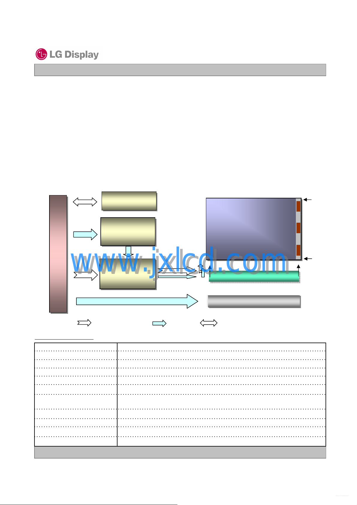
EDID
CN
BLOCK
1
1
User connector
www.jxlcd.com
40
www.jxlcd.com
Pin
Control & Data Power EDID signal & Power
POWER
BLOCK
LVDS &
Timing
Control
Block
PWM & VBL
General Features
11.6 inches diagonal Active Screen Size
268.0(H) × 169.0(V) × .3.6(D,Max.) [mm]Outline Dimension
0.1875mm × 0.1875 mmPixel Pitch
1366 horiz. By 768 vert. Pixels RGB strip arrangementPixel Format
6-bit, 262,144 colorsColor Depth
200 cd/m2(Typ.5 point)Luminance, White
Power Consumption
Ver. 1.0 Aug. 18, 2009
Total 3.01 Watt(Typ.) @ LCM circuit 0.9 Watt(Typ.), B/L input 2.11 Watt(Typ.)
(W/O LED Driver)
235g (Max.)Weight
Transmissive mode, normally whiteDisplay Operating Mode
Glare treatment of the front polarizerSurface Treatment
YesRoHS Comply
TFT-LCD Panel
(1366 x 768)
1
Source Driver Circuit
LED Backlight Ass’y
COG
768
1366
4 / 27
LP116WH2
www.DataSheet.net/
Datasheet pdf - http://www.DataSheet4U.co.kr/
Liquid Crystal Display
Product Specification
2. Absolute Maximum Ratings
The following are maximum values which, if exceeded, may cause faulty operation or damage to the unit.
Table 1. ABSOLUTE MAXIMUM RATINGS
60
Values
90% 80%
MaxMin
60
40
20
10
%
%
%
%
Parameter Notes
Power Input Voltage
Operating Temperature
Storage Temperature
Operating Ambient Humidity
Storage Humidity
Note : 1. Temperature and relative humidity range are shown in the figure below.
Wet bulb temperature should be 39°CMax, and no condensation of water.
www.jxlcd.com
www.jxlcd.com
Wet Bulb
Temperature [℃℃℃℃]
20
10
0
Symbol
OP
ST
OP
ST
50
40
30
Units
Humidity[(%)RH]
Storage
Operation
at 25 ± 5°CVdc4.0-0.3VCC
1°C500T
1°C60-20H
1%RH9010H
1%RH9010H
-20
Ver. 1.0 Aug. 18, 2009
10
20 30 40 50
Dry Bulb Temperature [℃℃℃℃]
60 70 800
5 / 27
LP116WH2
www.DataSheet.net/
Datasheet pdf - http://www.DataSheet4U.co.kr/
Liquid Crystal Display
Product Specification
3. Electrical Specifications
3-1. Electrical Characteristics
The LP116WH2 requires two power inputs. One is employed to power the LCD electronics and to drive the
TFT array and liquid crystal. The second input which powers the LED BL.
Table 2. ELECTRICAL CHARACTERISTICS
Parameter Symbol
MODULE :
Power Supply Input Current
Differential Impedance
LED Backlight ( With LED Driver ) :
LED Driver ( @12V )
Operating Voltage
Operating Current per string
Power Consumption
www.jxlcd.com
www.jxlcd.com
Note)
1. The specified current and power consumption are under the Vcc = 3.3V , 25℃, fv = 60Hz condition
whereas Mosaic pattern is displayed and fv is the frame frequency.
I
CC
Zm
DRIVER
LED
LED
BL
Values
MaxTypMin
3.63.33.0VCCPower Supply Input Voltage
315270225
V
DC
Watt0.140.12P
V3432-V
Hz10000-1000PWMPWM Frequency
%100-12.5PWM Duty
NotesUnit
1mA
1Watt1.050.9-PcPower Consumption
2Ohm11010090
3mA22-I
4Watt2.252.11-P
5Hrs15,000Life Time
2. This impedance value is needed to proper display and measured form LVDS Tx to the mating connector.
3. The typical operating current is for the typical surface luminance (LWH) in optical characteristics.
I
is the current of each LED’s string, LED backlight has 3 strings on it.
LED
4. The LED power consumption shown above does not include power of external LED driver circuit
for typical current condition.
5. The life time is determined as the time at which brightness of LED is 50% compare to that of initial value
at the typical LED current.
Ver. 1.0 Aug. 18, 2009
6 / 27
LP116WH2
www.DataSheet.net/
Datasheet pdf - http://www.DataSheet4U.co.kr/
Liquid Crystal Display
Product Specification
3-2. Interface Connection
This LCD employs one interface connection, a 40 pin connector is used for the module electronics interface.
Table 3. MODULE CONNECTOR PIN CONFIGURATION (CN1)
NotesDescriptionSymbolPin
Connector Test/No Connection(Reserved)CT1/NC1
+3.3V Power SupplyVDD2
+3.3V Power SupplyVDD3
4
6
7
EDID
EDID
EDID
www.jxlcd.com
www.jxlcd.com
NC No Connection21
Connector Test/No Connection(Reserved)CT2/NC34
System PWM signal input(+3.3V swing)S_PWMIN35
+3.3V EDID PowerV
Panel Self TestTest5
EDID Clock InputCLK
EDID Data InputDATA
LVDS differential data inputRxIN0-8
LVDS differential data inputRxIN0+9
GroundGND10
LVDS differential data inputRxIN1-11
LVDS differential data inputRxIN1+12
GroundGND13
LVDS differential data inputRxIN2-14
LVDS differential data inputRxIN2+15
GroundGND16
LVDS differential clock inputRxCLKIN-17
LVDS differential clock inputRxCLKIN+18
GroundGND19
No ConnectionNC20
GroundGND22
No ConnectionNC23
No ConnectionNC24
GroundGND25
No ConnectionNC26
No ConnectionNC27
GroundGND28
No ConnectionNC29
No ConnectionNC30
LED GroundVLED_GND31
LED GroundVLED_GND32
LED GroundVLED_GND33
LED Enable(3.3V Input)[Note 1]BL_ON36
No ConnectionNC37
5~20V LED Power SupplyVLED38
5~20V LED Power SupplyVLED39
5~20V LED Power SupplyVLED40
1, Interface chips
1.1 LCD : SiW, 1port including
LVDS Receiver
1.2 System :
* Pin to Pin compatible with LVDS
2. Connector
2.1 LCD :I-PEX 20455-040E-0*
(Locking type)
or equivalent
2.2 Mating :
2.3 Connector pin arrangement
40
[LCD Module Rear View]
[Note 1]
On: 2.0V↑,Off:0~0.4V
1
Ver. 1.0 Aug. 18, 2009
7 / 27
Product Specification
www.DataSheet.net/
Datasheet pdf - http://www.DataSheet4U.co.kr/
3-3. LVDS Signal Timing Specifications
3-3-1. DC Specification
LP116WH2
Liquid Crystal Display
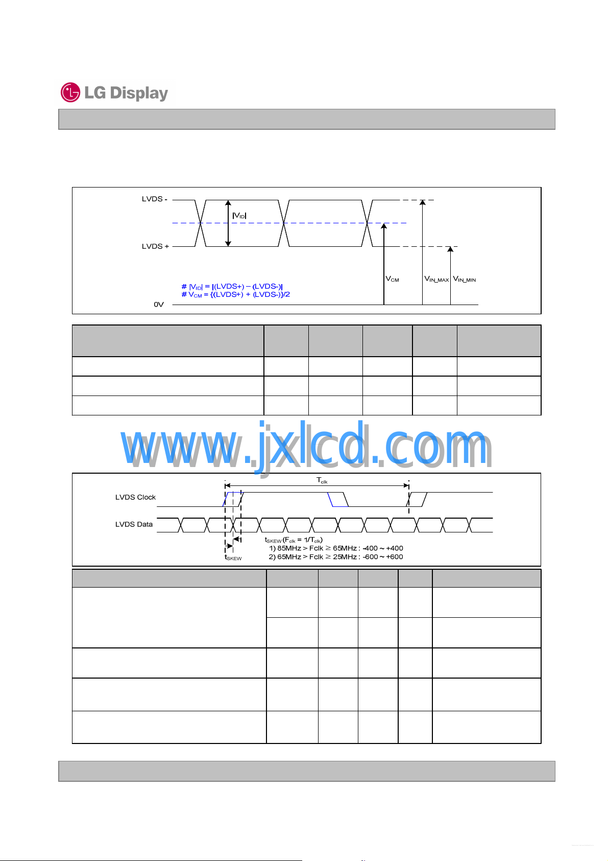
Description
LVDS Common mode Voltage
LVDS Input Voltage Range
3-3-2. AC Specification
LVDS Clock to Data Skew Margin
www.jxlcd.com
www.jxlcd.com
Symb
ol
CM
IN
SKEW
SKEW
- 600
NotesUnitMaxMin
-mV600100|VID|LVDS Differential Voltage
-V1.80.6V
-V2.10.3V
NotesUnitMaxMinSymbolDescription
ps+ 400- 400t
ps+ 600t
85MHz > Fclk ≥
65MHz
65MHz > Fclk ≥
25MHz
LVDS Clock to Clock Skew Margin (Even
to Odd)
Maximum deviation
of input clock frequency during SSC
Maximum modulation frequency
of input clock during SSC
Ver. 1.0 Aug. 18, 2009
SKEW_EO
DEV
MOD
- 1/7
+ 1/7t
T
clk
%± 3-F
KHz200-F
-
-
-
8 / 27
Freq.
www.DataSheet.net/
Datasheet pdf - http://www.DataSheet4U.co.kr/
F
max
F
center
F
min
Product Specification
< Clock skew margin between channel >
LP116WH2
Liquid Crystal Display
F
* F
center
DEV
www.jxlcd.com
www.jxlcd.com
3-3-3. Data Format
- LVDS 1 Port
RCLK+
RA+/-
RB+/-
RC+/-
RD+/-
R3 R2
G4 G3
B5 B4
G7 G6
R1 R0
G2 G1
B3 B2
R7 R6
1
F
MOD
< Spread Spectrum >
G0 R5 R4 R3 R2 R1 R0
B1 B0 G5 G4 G3 G2 G1
DE VSYNC HSYNC B5 B4 B3 B2
X B7 B6 G7 G6 R7 R6
Time
G0
B1
DE
VSYNC HSYNC
X
R5 R4
B0 G5
B7 B6
Previous (N-1)th Cycle Next(N+1)th Cycle
Current (Nth) Cycle
< LVDS Data Format >
Ver. 1.0 Aug. 18, 2009
9 / 27
 Loading...