

LG LN240 Service Manual
LN240
Features of LN240
1. Wave Type
CELLULAR : G7W
●
PCS: G7W
●
2. Frequency Scope
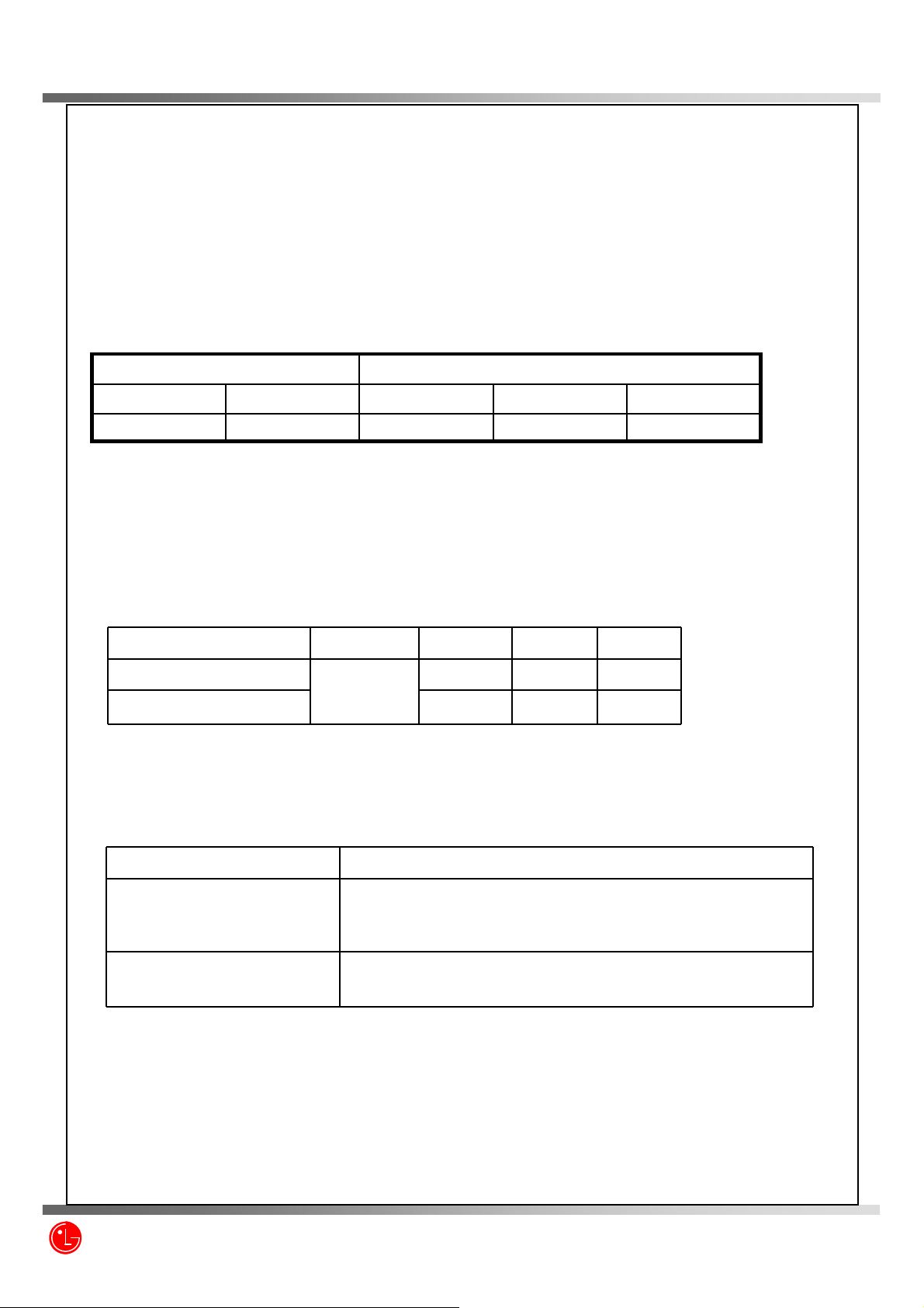
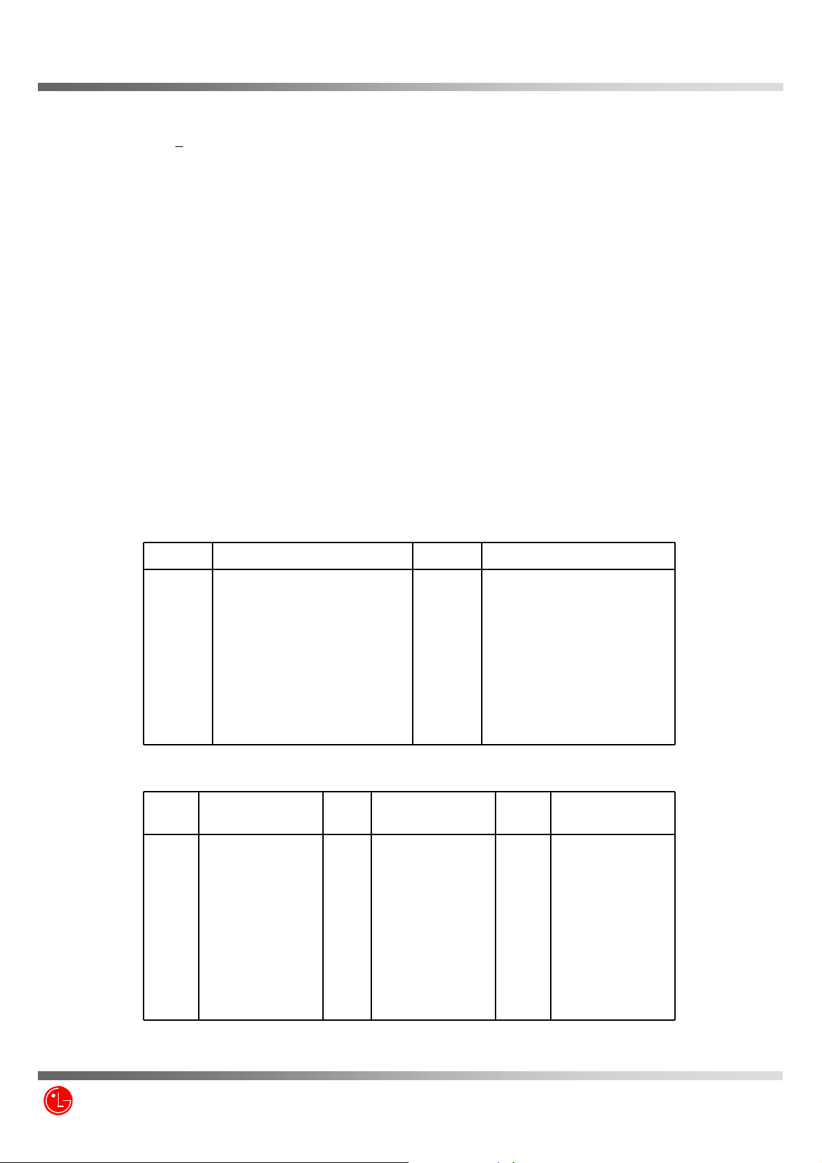
3. Rated Output Power : CELLULAR = 0.251W
PCS = 0.251W
Transmit Frequency (MHz)Transmit Frequency (MHz)
GPSPCSCELLULARPCSCELLULAR
1575.421930~1990869.82~893.191850~1910824.82 ~ 848.19
4. Output Conversion Method : This is possible by correcting the key board channel.
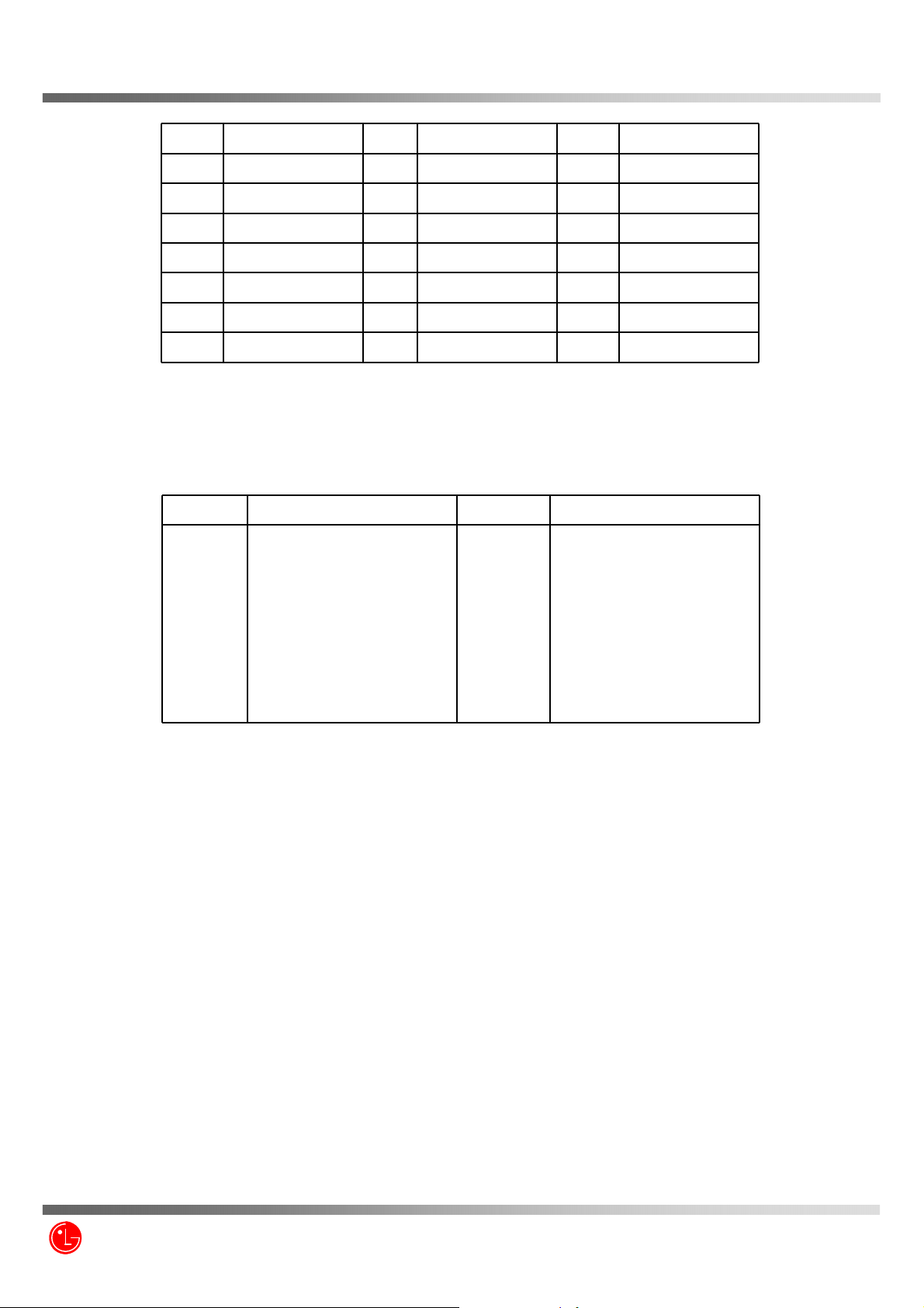
5. Voltage and Current Value of Termination Part Amplifier (Catalogue included)
MODE Part Name Voltage Current Power
CELLULAR
ACPM7353
PCS 4.2V 700mA 0.251W
6. Functions of Major Semi-Conductors
Classification Function
QSC6055 Terminal operation control and digital signal processing
Converts RF signal to baseband signal
Converts baseband signal to RF signal
MCP (TY9A0A111110KC) NAND (1Gbit) + DDR (512Mbit)
Storing of terminal operation program
4.2V 700mA 0.251W
7. Frequency Stability
CELLULAR : ±0.5PPM
●
● PCS : ±0.1PPM
LG Electronics Inc.
1/169
LN240
CDMA Mobile Subscriber Unit
LN240
SERVICE MANUAL
SERVICE MANUAL
Triple BAND, Triple Mode
[PCS/Cellular/GPS]
CDMA MOBILE PHONE
LG Electronics Inc.
2/169

LN240
Table of Contents
General Introduction……………………………………………………………………………...4
CHAPTER 1. System Introduction
1. CDMA Abstract…….………………………………………………………………….…….…..5
2. Features and Advantages of CDMA Mobile Phone…………....................................................6
3. Structure and Functions of Tri-Band CDMA Mobile Phone……………………...……….….9
4. Specification…………………………………………………………………………..…………10
5. Installation………………………………………………………………………………………16
CHPATER 2. NAM Input Method
1. NAM Program Method and Telephone Number Inputting Method……………..…………18
CHAPTER 3. Circuit Description
1. RF Transmit/Receive Part………………………………………………………….…….……21
2. Digital/Voice Processing Part………………………………………………………………….32
CHAPTER 4. Trouble Shooting
4.1. RX PART TROUBLE....………………………………………………..…………………...36
4.2. TX PART TROUBLE....……………………………………………………..……………...54
4.3. POWER PART TROUBLE………………………………………………….………..….....80
CHAPTER 5. Safety…………………………………………………….……………..…… 112
CHAPTER 6. Glossary………………………………………………….…………………. 115
APPENDIX ……………………………………………………..……... 127
1. Block Diagram ……………………………………………………………….……….128
2. Circuit diagram……………………………………………………………………..…129
3. Component Layout……………………………………………………………………137
4. Exploded View ……………………………………………………………….……….144
5. Part list (Mechanical) …………….……………………………………………..…...146
6. Part List(Circuit)……………………………………………………………..……….149
7. BGA PIN MAP…………………………………………………………………..……..165
LG Electronics Inc.
3/169
LN240
General Introduction
General Introduction
The LfN240 phone has been designed to operate on the latest digital mobile communication technology, Code
Division Multiple Access (CDMA). This CDMA digital technology has greatly enhanced voice clarity and can
provide a variety of advanced features. Currently, CDMA mobile communication technology has been
commercially used in Cellular and Personal Communication Service (PCS). The difference between them is the
operating frequency spectrum. Cellular uses 800MHz and PCS uses 1.9GHz. The LN240 support GPS Mode, we
usually call it tri-band phone. Also, LN240 works on Advanced Mobile Phone Service (S-GPS). We call it dualmode phone. If one of the Cellular, PCS base stations is located nearby, Call fail rate of triple-mode phone is less
than dual-mode phone or single-mode phone.
The CDMA technology adopts DSSS (Direct Sequence Spread Spectrum). This feature of DSSS enables the phone
to keep communication from being crossed and to use one frequency channel by multiple users in the same specific
area, resulting that it increases the capacity 1 0 times more co mpar ed with that in the analog mode currently used.
Soft/Softer Handoff, Hard Handoff, and Dynamic RF power Control technologies are combined into this phone to
reduce the call being interrupted in a middle of talking over the phone.
Cellular and PCS CDMA network consists of MSO (Mobile Switching Office), BSC (Base Station Controller), BTS
(Base station Transmission System), and MS (Mobile Station). The following table lists some major CDMA
Standards.
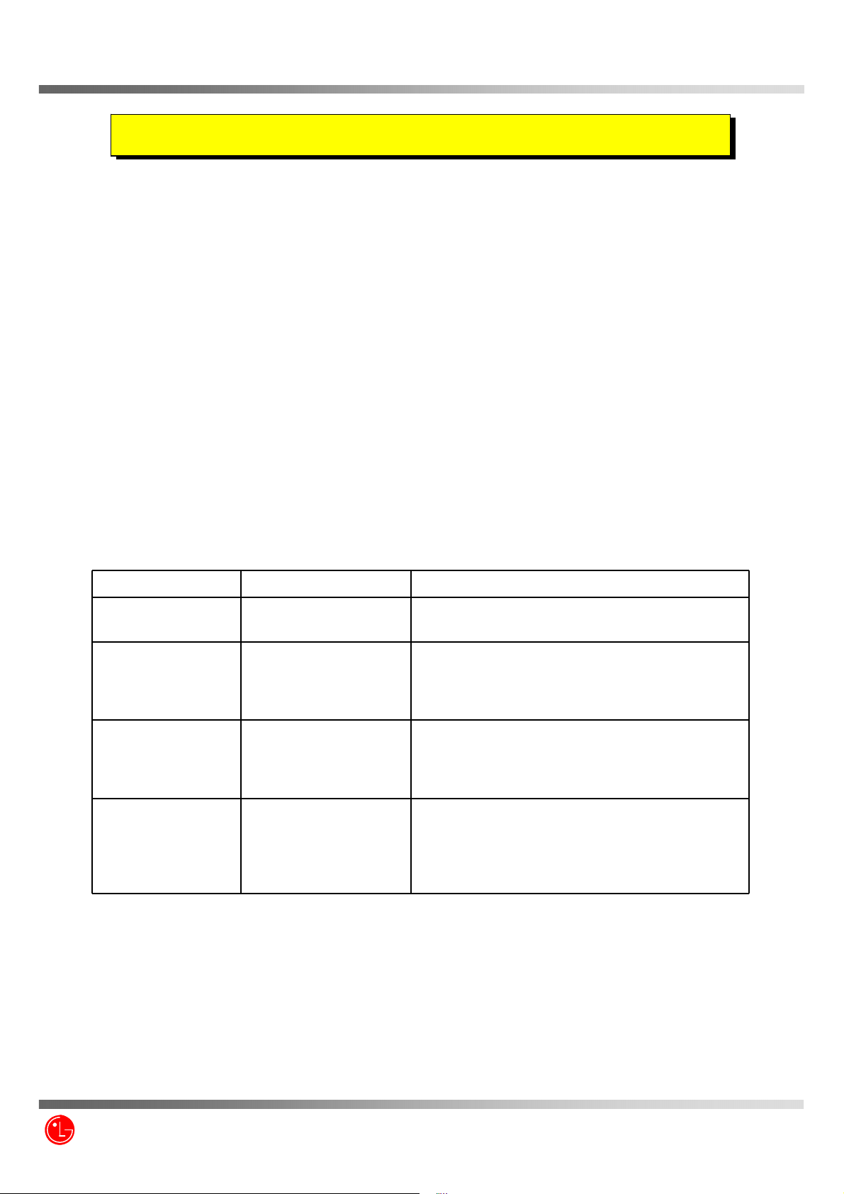
CDMA Standard Designator Description
Basic air interface TIA/EIA/IS-95-A/B/C
ANSI J-STD-008
Network TIA/EIA/IS-634
TIA/EIA/IS/651
TIA/EIA/IS-41-C
TIA/EIA/IS-124
Service TIA/EIA/IS-96-B
TIA/EIA/IS-99
TIA/EIA/IS-637
TIA/EIA/IS-657
Performance TIA/EIA/IS-97
TIA/EIA/IS-98
ANSI J-STD-018
ANSI J-STD-019
TIA/EIA/IS-125
* TSB –74: Protocol between an IS-95A system and ANSI J-STD-008
Protocol between MS and BTS for Cellular & AMPS
Protocol between MS and BTS for PCS
MAS-BS
PCSC-RS
Intersystem operations
Nom-signaling data comm.
Speech CODEC
Assign data and fax
Short message service
Packet data
Cellular base station
Cellular mobile station
PCS personal station
PCS base station
Speech CODEC
LG Electronics Inc.
4/169

LN240
Chapter1. System Introduction
Chapter1. System Introduction
1. CDMA Abstract
The CDMA mobile communication system has a channel hand-off function that is used for collecting the information
on the locations and movements of mobile telephones from the cell site by auto matically controlling several cell site
through the setup of data transmission routes, and then enabling one switching system to carry out the automatic
remote adjustment. This is to maintain continuously the call state through the automatic location co nfirmation and
automatic radio channel conversion when the busy subscriber moves from the service area of one cell site to that of
another by using automatic location confirmation and automatic radio channel conversion functions. The call state
can be maintained continuously by the information exchange between switching systems when the busy subscriber
moves from one Cellular system area to the other Cellular system area.
In the Cellular system, the cell site is a small-sized low output type and utilizes a frequency allocation system that
considers mutual interference, in an effort to enable the re-use of corresponding frequency from a cell site separated
more than a certain distance.
Unlike the time division multiple access (TDMA) or frequency division multiple access (FDMA) used in the band
limited environment, the Code Division Multiple Access (CDMA) system which is one of digital Cellular systems is
a multi-access technology under the interference limited environment. It can process more number of subscribers
compared to other systems (TDMA system has the processing capacity three times greater than the existing FDMA
system whereas CDMA system, about 12~15 times of that of the existing system).
CDMA system can be explained as follows; TDMA or CDMA can be used to enable each person to talk alternately
or provide a separate room for each person when two persons desire to talk with each other at the same time, whereas
FDMA can be used to enable one person to talk in soprano, whereas the other in bass (one of the two talkers can
carry out synchronization for hearing in case there is a bandpass filter function in the area of the hearer). Another
available method is to make two persons to sing in different languages at the same time, space, and frequency when
wishing to let the audience hear the singing without being confused. This is the characteristic of CDMA.
On the other hand, when employing the CDMA technology, each signal has a different pseudo-random binary
sequence used to spread the spectrum of carrier. A great number of CDMA signals share the same frequency
spectrum. In the perspective of frequency area or time area, several CDMA signals are overlapped. Among these
types of signals, only desired signal energy is selected and received through the use of pre-determined binary
sequence; desired signals can be separated, and then received with the correlators used for recovering the spectrum
into its original state. At this time, the spectrums of other signals that have different codes are not recovered into its
original state, and appears as the self-interference of the system.
LG Electronics Inc.
5/169

LN240
2. Features and Advantages of CDMA Mobile Phone
2.1 Various Types of Diversities
When employing the narrow band modulation (30kHz band) that is the same as the analog FM modulation system
used in the existing Cellular system, the multi-paths of radio waves create a serious fading. However, in the CDMA
broadband modulation (1.25MHz band), three types of diversities (time, frequency, and space) are used to reduce
serious fading problems generated from radio channels in order to obtain high-quality calls.
Time diversity can be obtained through the use of code interleaving and error correction code whereas frequency
diversity can be obtained by spreading signal energy to wider frequency band. The fading related to normal
frequency can affect the normal 200~300KHz among signal bands and accordingly, serious effect can be avoided.
Moreover, space diversity (also called path diversity) can be realized with the following three types of methods.
First, it can be obtained by the duplication of cell site receive antenna. Second, it can be obtained through the use of
multi-signal processing device that receives a transmit signal having each different transmission delay time and then,
combines them. Third, it can be obtained through the multiple cell site connection (Soft Handoff) that connects the
mobile station with more than two cell sites at the same time.
2.2 Power Control
The CDMA system utilizes the forward (from a base station to mobile stations) and backward (from the mobile
station to the base station) power control in order to increase the call processing capacity and obtain high-quality calls.
In case the originating signals of mobile stations are received by the cell site in the minimum call quality level (signal
to interference) through the use of transmit power con trol on all the mobile stations, the syste m capacity can be
maximized. If the signal power of mobile station is received too strong, the performance of that mobile station is
improved. However, because of this, the interference on other mobile stations using the same channel is increased
and accordingly, the call quality of other subscribers is reduced unless the maximum accommodation capacity is
reduced.
In the CDMA system, forward power control, backward open loop power control, and closed loop power control
methods are used. The forward power control is carried out in the cell site to reduce the transmit power on mobile
stations less affected by the multi-path fading and shadow phenomenon and the interference of other cell sites when
the mobile station is not engaged in the call or is relatively nearer to the corresponding cell site. This is also used to
provide additional power to mobile stations having high call error rates, located in bad reception areas or far away
from the cell site.
The backward open loop power control is carried out in a corresponding mobile station; the mobile station measures
power received from the cell site and then, reversely increases/decreases transmit power in order to compensate
channel changes caused by the forward link path loss and terrain characteristics in relation to the mobile station in the
cell site. By doing so, all the mobile transmit signals received by the base station have same strength.
Moreover, the backward closed loop power control used by the mobile station is performed to control power using
the commands issued out by the cell site. The cell site receives the signal of each corresponding mobile station and
compares this with the pre-set threshold value and then, issues out power increase/decrease commands to the
corresponding mobile station every 1.25msec (800 times per second). By doing so, the gain tolerance and the
different radio propagation loss on the forward/backward link are complemented.
LG Electronics Inc.
6/169

LN240
2.3 Voice Encoder and Variable Data Speed
The bi-directional voice service having variable data speed provides voice communication which employs voice
encoder algorithm having power variable data rate between the base station and the mobile station. On the other hand,
the transmit voice encoder performs voice sampling and then, creates encoded voice packets to be sent out to the
receive voice encoder, whereas the receive voice encoder demodulates the received voice packets into voice samples.
One of the two voice encoders described in the above is selected for use depending on inputted automatic conditions
and message/data; both of them utilize four-stage frames of 9600, 4800, 2400 , and 1200 bits per second for Cellular
and 14400,7200,3600,1800 bits per second for PCS, so PCS provide relatively better voice quality (almost twice
better than the existing cellular system). In addition, this type of variable voice encoder u tilizes adaptive threshold
values on selecting required data rate. It is adjusted in accordance with the size of background noise and the data rate
is increased to high rate only when the voice of caller is inputted.
Therefore, background noise is suppressed and h igh-qu ality voice transmission is possible under the environment
experiencing serious noise. In addition, in case the caller does not talk, data transmission rate is reduced so that the
transmission is carried out in low energy. This will reduce the interference on other CDMA signals and as a result,
improve system performance (capacity increased by about two times).
2.4 Protecting Call Confidentiality
Voice privacy is provided in the CDMA system by means of the private long code mask used for PN spreading.
Voice privacy can be applied on the traffic channels only. All calls are initiated using the public long code mask for
PN spreading. The mobile station user may request voice privacy during call setup using the origination message or
page response message, and during traffic channel operation using the long code transition request order.
The Transition to private long code mask will not be performed if authentication is not performed. To initiate a
transition to the private or public long code mask, either the base station or the mobile station send s a long code
transition request order on the traffic channel.
2.5 Soft Handoff
A handoff in which the mobile station commences communications with a new base station without interrupting
communications with the old base station. Soft handoff can only be used between CDMA channels having identical
frequency assignments.
2.6 Frequency Re-Use and Sector Segmentation
Unlike the existing analog Cellular system, the CDMA system can reuse the same frequency at the adjacent cell.
there is no need to prepare a separate frequency plan. Total interference generated on mobile station signals received
from the cell site is the sum of interference generated from other mobile stations in the same cell site and interference
generated from the mobile station of adjacent cell site. That is, ea ch mobile station signal generates interference in
relation to the signals of all the other mobile stations.
LG Electronics Inc.
7/169

LN240
Total interference from all the adjacen t cell sites is the ratio of interference from all the cell sites versus total
interference from other mobile stations in the same cell site (about 65%). In the case of directional cell site, one cell
normally uses a 120°sector antenna in order to divide the sector into three. In this case, each antenna is used only for
1/3 of mobile stations in the cell site and accordingly, interference is reduced by 1/3 on the average and the capacity
that can be supported by the entire system is increased by three times.
2.7 Soft Capacity
The subscriber capacity of the CDMA system is flexible depending on the relation between the number of users and
service classes. For example, the system operator can increase the number of channels available for use during the
busy hour despite the drop in call quality. This type of function requires 40% o f normal call channels in the standby
mode during the handoff, in an effort to avoid call disconnection resulting from the lack of channels.
In addition, in the CDMA system, services and service charges are classified further into different classes so that
more transmit power can be allocated to high class service users for easier call set-up; they can also be given higher
priority of using hand-off function than the general users.
LG Electronics Inc.
8/169

LN240
3. Structure and Functions of Tri-band CDMA Mobile Phone
The hardware structure of CDMA mobile phone is made up of radio frequency (RF) part and logic part. The RF part
is composed of Receiver part (Rx), Transmitter part (Tx) and Local part (LO). For the purpose of operating on triband, It is necessary dual Tx path, tri Rx path, dual PLL and switching system for band selection. The mobile phone
antenna is connected with the frequency separator which divide antenna input/output signals between Cellular
frequency band (824~894 MHz) and PCS frequency band (1850~1990MHz). Each separated path is linked with the
Cellular duplexer and PCS duplexer. Duplexer carries out separating Rx band and Tx band. The Rx signals from the
antenna are converted into intermediate frequency(IF) band by the frequency synthesizer and frequency down
converter. And then, pass SAW filter which is a band pass filter for removing out image frequency. The IF output
signals that have been filtered is converted into digital signals via Analog-to-Digital Converter (ADC). In front of the
ADC, switching system is required to choose which band path should be open. The digital signals send to 5
correlators in each CDMA de-modulator. Of these, one is called a searcher whereas the remaining 4 are called data
receivers (fingers). Digitalized IF signals include a great number of call signals that have been sent out by the
adjacent cells. These signals are detected with pseudo-noise sequence (PN Sequence). Signal to interference ratio
(C/I) on signals that match the desired PN sequence are increased through this type of cor relation detection process,
but other signals obtain processing gain by not increasing the ratio. The carrier wave of pilot channel from the cell
site most adjacently located is demodulated in order to obtain the sequence of encoded data symbols. During the
operation with one cell site, the searcher searches ou t multi-paths in ac cordance with terrain and building reflections.
On three data receivers, the most powerful 3 paths are allocated for the parallel tracing and receiving. Fading
resistance can be improved a great deal by obtaining the diversity combined output for de-modulation. Moreover, the
searcher can be used to determine the most powerful path from the cell sites even during the soft handoff between the
two cell sites. Moreover, 3 data receivers are alloc ated in order to carry out the de-modulation of these paths. Output
data that has been demodulated changes the data string in the combined data row as in the case of original
signals(deinterleaving), and then, are demodulated by the forward error correction decoder which uses the Viterbi
algorithm.
Mobile station user information send out from the mobile station to the cell site pass through the digital voice
encoder via a mike. Then, they are encoded and forward errors are corrected through the use of convolution encoder.
Then, the order of code rows is changed in accordance with a certain regulation in order to remove any errors in the
interleaver. Symbols made through the above process are spread after being loaded onto PN carrier waves. At this
time, PN sequence is selected by each address designated in each call.
Signals that have been code spread as above are digital modulated (QPSK) and then, power controlled at the
automatic gain control amplifier (AGC Amp). Then, they are converted into RF band by the frequency synthesizer
synchronizing these signals to proper output frequencies.
Transmit signals obtained pass through the duplexer filter and then, are sent out to the cell site via the antenna.
LG Electronics Inc.
9/169
LN240
4. Specification
4.1 General Specification
4.1.1 Transmit/Receive Frequency Interval :
1) CELLULAR : 45 MHz
2) PCS : 80 MHz
4.1.2 Number of Channels (Channel Bandwidth)
1) CELLULAR : 20 Channels
2) PCS : 48 Channels
4.1.3 Operating Voltage : DC 3.2~4.2V
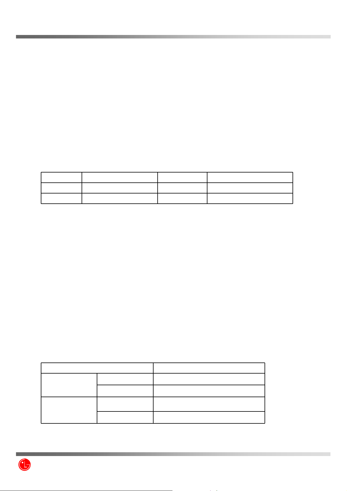
4.1.4 Battery Power Consumption : DC 3.7V
SLEEP IDLE MAX POWER
CELLULAR 1.5 mA 150mA 700 mA (24.5 dBm)
PCS 1.5 mA 150mA 700 mA (24.5 dBm)
4.1.5 Operating Temperature : -20°C ~ +50°C
4.1.6 Frequency Stability
1) CELLURAR : ±0.5PPM
2) PCS : ±0.1PPM
4.1.7 Antenna : Internal Antenna, 50
4.1.8 Size and Weight
1) Size : 88x63x15.8mm
2) Weight :108g
4.1.9 Channel Spacing
1) CELLULAR : 1.25MHz
2) PCS : 1.25 MHz
4.1.10 Battery Type, Capacity and Operating Time. Unit = Hours : Minutes
Standby Time
Talk Time
LG Electronics Inc.
Standard (900mAh)
PCS (Slot Cycle 2) About 170 Hrs (SCI=2)
DCN (Slot Cycle 2) About 170 Hrs (SCI=2)
PCS (Slot Cycle 2) 180 Min .(typical duplexer,10dBm output)
DCN (Slot Cycle 2) 180 Min .(typical duplexer,10dBm output)
10/169

LN240
4.2 Receive Specification
4.2.1 Frequency Range
1) CELLULAR : 869.820 MHz ~ 893.190 MHz
2) PCS : 1930 MHz ~ 1990 MHz
3) GPS : 1575.42 MHz
4.2.2 Local Oscillating Frequency Range :
1) CELLULAR : 3404.0 MHz ~ 3576.0 MHz
2) PCS : 3860.0 MHz ∼ 4000.0 MHz
3) GPS : 3150.84 MHz
4.2.3 Sensitivity
1) CELLULAR : -104dBm (C/N 12dB or more)
2) PCS : -104dBm (C/N 12dB or more)
3) GPS : -148.5dBm
4.2.4 Selectivity
1) CELLULAR : 3dB C/N Degration (With Fch±1.25 kHz : -30dBm)
2) PCS : 3dB C/N Degration (With Fch±1.25 kHz : -30dBm)
4.2.5 Interference Rejection
1) Single Tone : -30dBm at 900 kHz (CELLULAR), -30dBm at 1.25MHz (PCS)
2) Two Tone : -43dBm at 900 kHz & 1700kHz (CELLULAR), -43dBm at 1.25 MHz & 2.05 MHz (PCS)
4.2.6 Spurious Wave Suppression : Maximum of -80dB
4.2.7 CDMA Input Signal Range
Dynamic area of more than -104~ -25 dB: 79dB at the 1.23MHz band.
4.3 Transmit Specification
4.3.1 Frequency Range
1) CELLULAR : 824.820MHz ~ 848.190MHz
2) PCS : 1850 MHz ~ 1910 MHz
4.3.2 Output Power
1) CELLULAR : 0251W
2) PCS: 0.251W
LG Electronics Inc.
11/169
LN240
4.3.3 CDMA TX Frequency Deviation :
1) CELLULAR: +300Hz or less
2) PCS: ± 150Hz
4.3.4 CDMA TX Conducted Spurious Emissions
1) CELLULAR: 900kHz : - 42 dBc/30kHz below
1.98MHz : - 54 dBc/30kHz below
2) PCS : 1.25MHz: - 42 dBc/30kHz below
1.98MHz : - 50 dBc/30kHz below
4.3.5 CDMA Minimum TX Power Control
1) CELLULAR: - 50dBm below
2) PCS: -50dBm below
4.4 MS (Mobile Station) Transmitter Frequency
4.4.1 CELLULAR mode
Ch # Center Freq. (MHz) Ch # Center Freq. (MHz)
1011
29
70
111
152
193
234
275
316
363
4.4.2 PCS mode
Ch # Center Freq
25 1851.25 425 1871.25 825 1891.25
50 1852.50 450 1872.50 850 1892.50
75 1853.75 475 1873.75 875 1893.75
(MHz)
824.640
825.870
827.100
828.330
829.560
830.790
832.020
833.250
834.480
835.890
404
445
486
527
568
609
650
697
738
779
Ch # Center Freq
(MHz)
837.120
838.350
839.580
840.810
842.040
843.270
844.500
845.910
847.140
848.370
Ch # Center Freq
(MHz)
100 1855.00 500 1875.00 900 1895.00
125 1856.25 525 1876.25 925 1896.25
150 1857.50 550 1877.50 950 1897.50
175 1858.75 575 1878.75 975 1898.75
LG Electronics Inc.
12/169
LN240
200 1860.00 600 1880.00 1000 1900.00
225 1861.25 625 1881.25 1025 1901.25
250 1862.50 650 1882.50 1050 1902.50
275 1863.75 675 1883.75 1075 1903.75
300 1865.00 700 1885.00 1100 1905.00
325 1866.25 725 1886.25 1125 1906.25
350 1867.50 750 1887.50 1150 1907.50
375 1868.75 775 1888.75 1175 1908.75
4.5 MS (Mobile Station) Receiver Frequency
4.5.1 CELLULAR mode
Ch. # Center Freq. (MHz) Ch. # Center Freq. (MHz)
1011
29
70
111
152
193
234
275
316
363
869.640
870.870
872.100
873.330
874.560
875.790
877.020
878.250
879.480
880.890
404
445
486
527
568
609
650
697
738
779
882.120
883.350
884.580
885.810
887.040
888.270
889.500
890.910
892.140
893.370
LG Electronics Inc.
13/169
LN240
4.5.2 PCS mode
Center Freq
Ch #
25 1931.25 425 1951.25 825 1971.25
50 1932.50 450 1952.50 850 1972.50
75 1933.75 475 1953.75 875 1973.75
100 1935.00 500 1955.00 900 1975.00
125 1936.25 525 1956.25 925 1976.25
150 1937.50 550 1957.50 950 1977.50
175 1938.75 575 1958.75 975 1978.75
200 1940.00 600 1960.00 1000 1980.00
225 1941.25 625 1961.25 1025 1981.25
250 1942.50 650 1962.50 1050 1982.50
275 1943.75 675 1963.75 1075 1983.75
300 1945.00 700 1965.00 1100 1985.00
325 1946.25 725 1966.25 1125 1986.25
350 1947.50 750 1967.50 1150 1987.50
(MHz)
Ch # Center Freq
(MHz)
Ch # Center Freq
(MHz)
375 1948.75 775 1968.75 1175 1988.75
LG Electronics Inc.
14/169

LN240
4.5.4 GPS mode : 1575.42 MHz
4.5.5 Bluetooth mode : 2400 MHz ~ 2483.5 MHz
4.6 AC Adaptor : See Appendix
4.7 Cigar Lighter Charger : See Appendix
4.8 Hand-Free Kit : See Appendix
LG Electronics Inc.
15/169

LN240
5. Installation
5.1 Installing a Battery Pack
1) The Battery pack is keyed so it can only fit one way. Align the groove in the battery pa ck with the rail on the back
of the phone until the battery pack rests flush with the back of the phone.
2) Slide the battery pack forward until you hear a “click”, which locks the battery in place.
5.2 For Adapter Use
1) Plug the adapter into a wall outlet. The adapter can be operated from a 110~220V source. When AC power is
connected to the adapter.
2) Insert the adapter IO plug into the phone with the installed battery pack.
.
5.3 For Mobile Mount
5.3.1 Installation Position
In order to reduce echo sound when using the Hands-Free Kit, make sure that the speaker and microphone are not
facing each other and keep microphone a generous distance from the speaker.
5.3.2 Cradle Installation
Choose an appropriate flat surface where the unit will not interface with driver’s movement or passenger’s comfort.
The driver/user should be able to access the phone with ease. Using the four self-tapping screws provided, mount the
supplied bracket on the selected area. Then with the four machine screws provided, mount the counterpart on the
reverse side of the reverse side of the cradle. Secure the two brackets firmly together by using the two bracket joint
screws provide. The distance between the cradle and the interface box must not exceed the length of the main cable.
5.3.3 Interface Box
Choose an appropriate flat surface ( somewhere under the dash on the passenger side is preferred ) and mount the IB
bracket with the four self-tapping screws provided. Clip the IB into the IB bracket.
5.3.4. Microphone Installation
Install the microphone either by clipping I onto the sunvisor (driver’s side) or by attaching it to door post (driver’s
side), using a velcro adhesive tape (not included).
5.3.5 Cable Connections
LG Electronics Inc.
16/169

LN240
5.3.5.1 Power and Ignition Cables
Connect the red wire to the car battery positive terminal and the black wire to the car ground. Connect the green wire
to the car ignition sensor terminal. ( In order to operate HFK please make sure to connect green wire to ignition
sensor terminal.) Connect the kit’s power cable connector to the interface box power receptacle.
5.3.5.2 Antenna Cable Connection
Connect the antenna coupler cable connector from the cradle to the external antenna connector. ( Antenna is not
included.)
LG Electronics Inc.
17/169
LN240
CHAPTER 2. NAM Input Method
CHAPTER 2. NAM Input Method
(Inputting of telephone numbers included)
(Inputting of telephone numbers included)
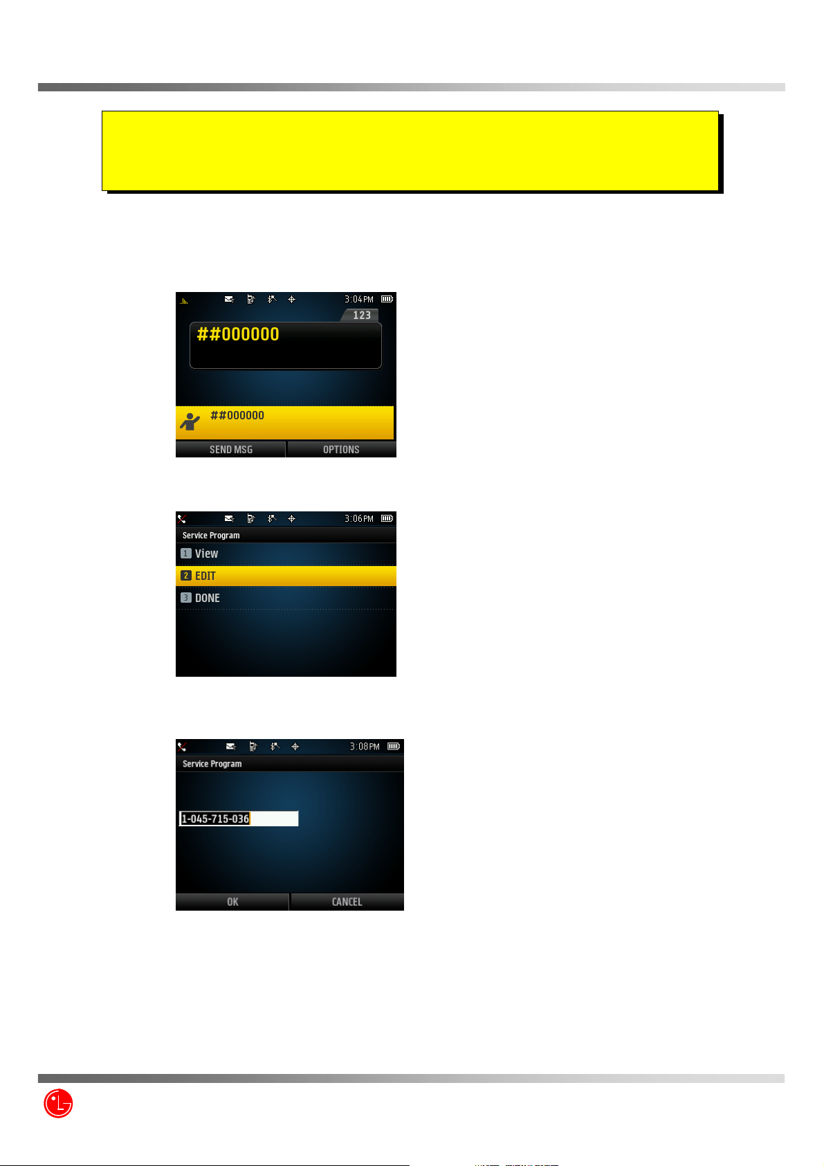
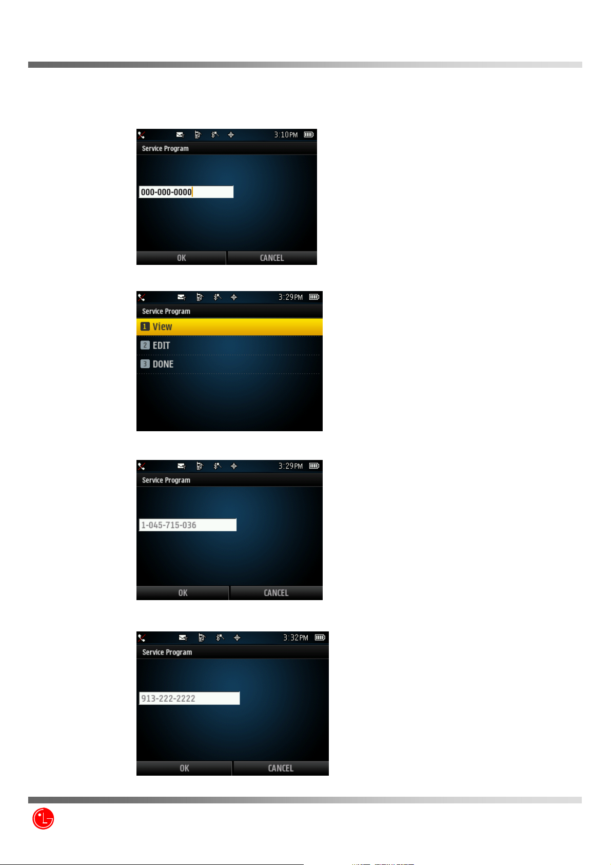
1.Press ##(6 digit Service Code)#
2. Select [Edit]
3. Enter MDN and Press OK
LG Electronics Inc.
18/169
LN240
4. Enter MSID and press OK.
5. Select [View] to check MDN & MSID
6. Check saved MDN and Press OK to check MSID
7. Check saved MSID and Press OK to exit [View]
LG Electronics Inc.
19/169
LN240
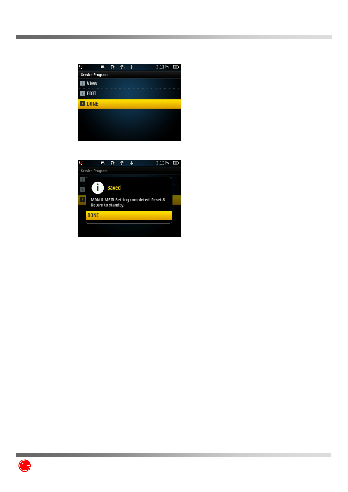
8. Select [DONE]
9. Saved & Reset
LG Electronics Inc.
20/169

LN240
CHAPTER 3. Circuit Description
CHAPTER 3. Circuit Description
1. RF Transmit/Receive Part
1.1 Overview
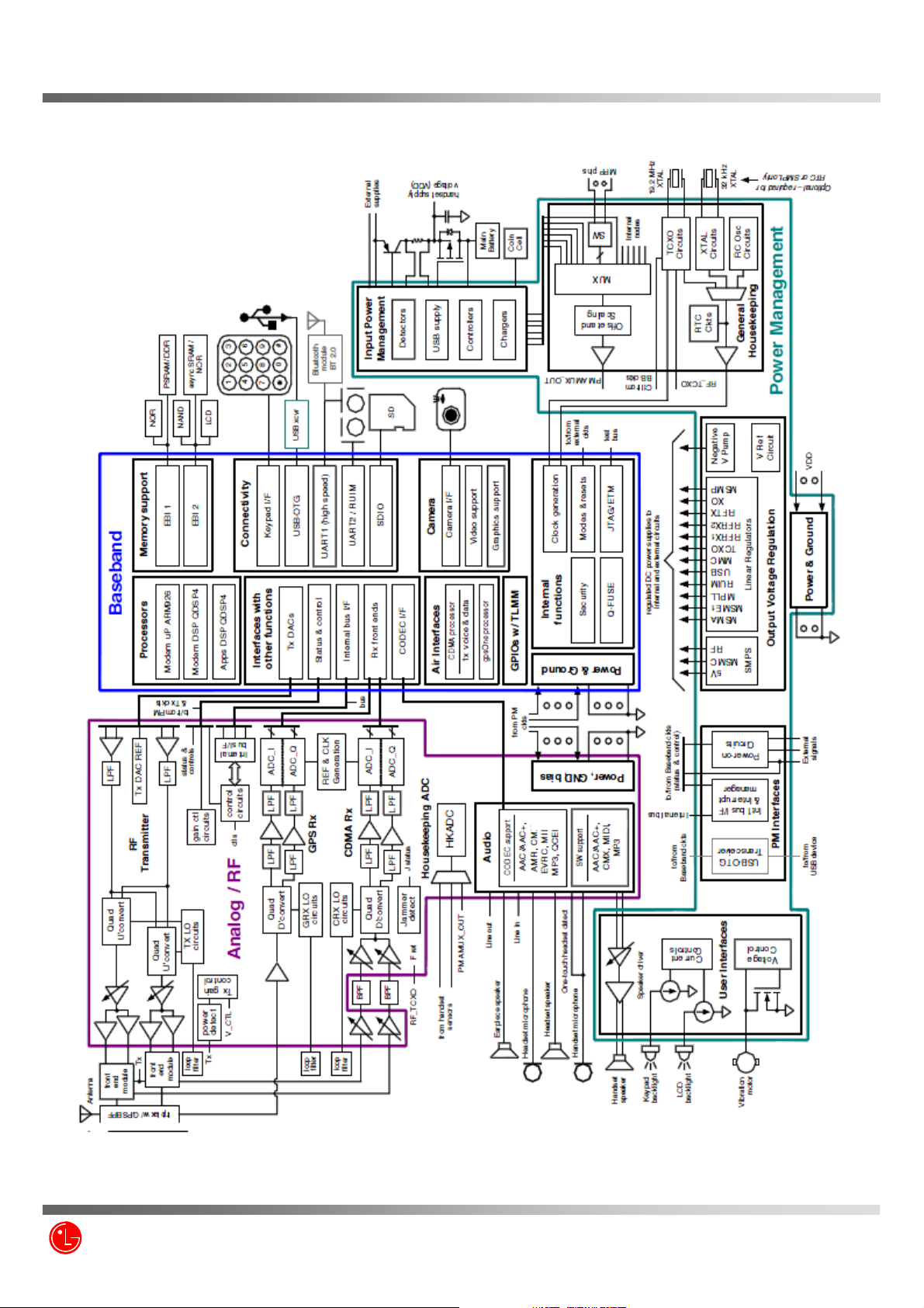
The Tx and Rx part employs the Direct Conversion system. The Tx and Rx frequencies are respectively
824.04~848.97MHz and 869.04~893.97MHz for cellular and 1850~1910MHz and 1930~1990MHz for
PCS .The block diagram is shown in [Figure 1-1]. RF signals received through the antenna are seperated
by quadplexer. RF Signal fed into the low noise amplifier (in QSC6055) through the quadplexer. Then, they
are combined with the signals of local oscillator (VCO) at the down conversion mixer (in QSC6055) in
order to create Base-band frequency. Then, this signal is changed into digital signal by the analog to digital
converter (ADC, A/D Converter), and the digital circuit part of the QSC (Qualcomm Single Chip) 6055
processes the data from ADC. The digital processing part is a demodulator.
In the case of transmission, RF transmitter (in QSC6055) receives QPSK-modulated analog signal from
the QSC6055. In QSC6055, the baseband quadrature signals are upconverted to the Cellular or PCS
frequency bands and amplified to provide signal drive capability to the power amp.
After that, the RF signal is amplified by the Power Amp in order to have enough power for radiation. Finally,
the RF signal is sent out to the cell site via the antenna after going through the coupler and quadplexer.
LG Electronics Inc.
21/169
LN240
[Figure 1-1] Block Diagram of LN240
LG Electronics Inc.
22/169
LN240
1.2 Description of Rx Part Circuit
1.2.1
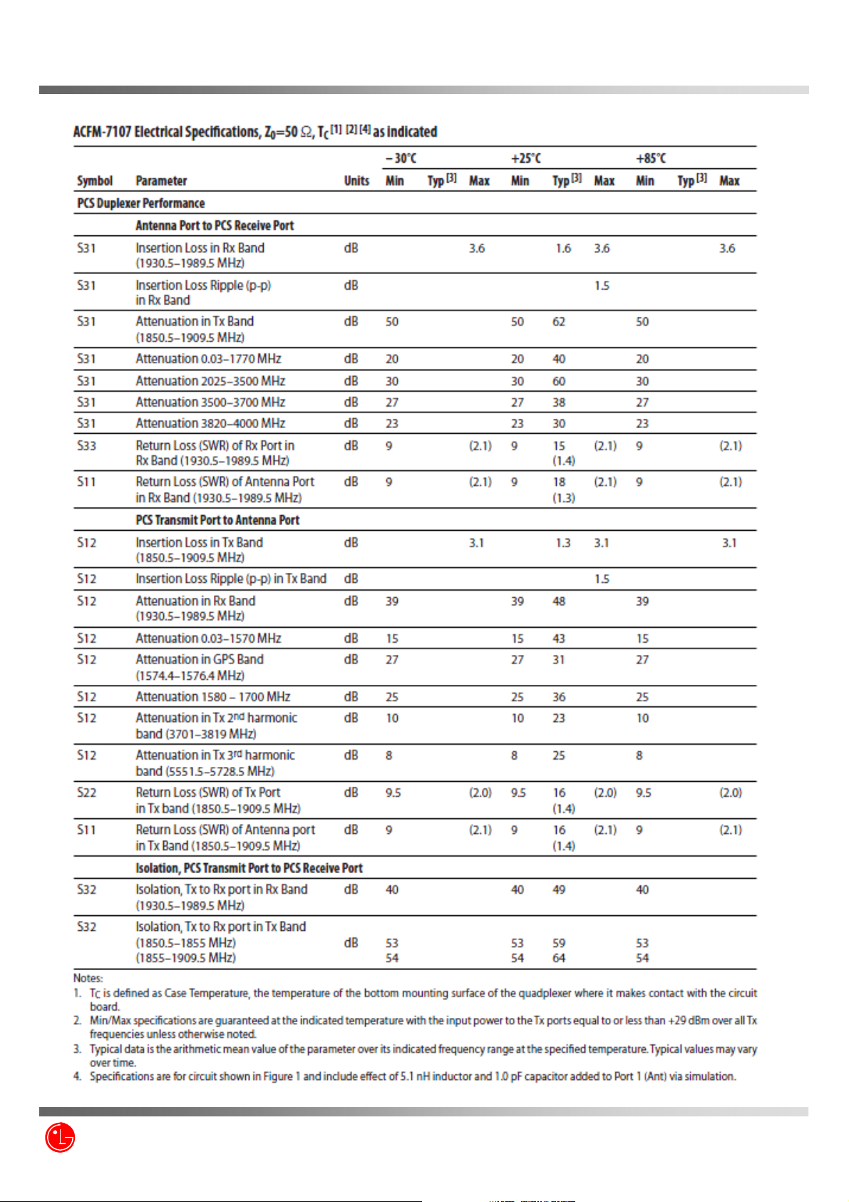
Quadplexer (U1502)
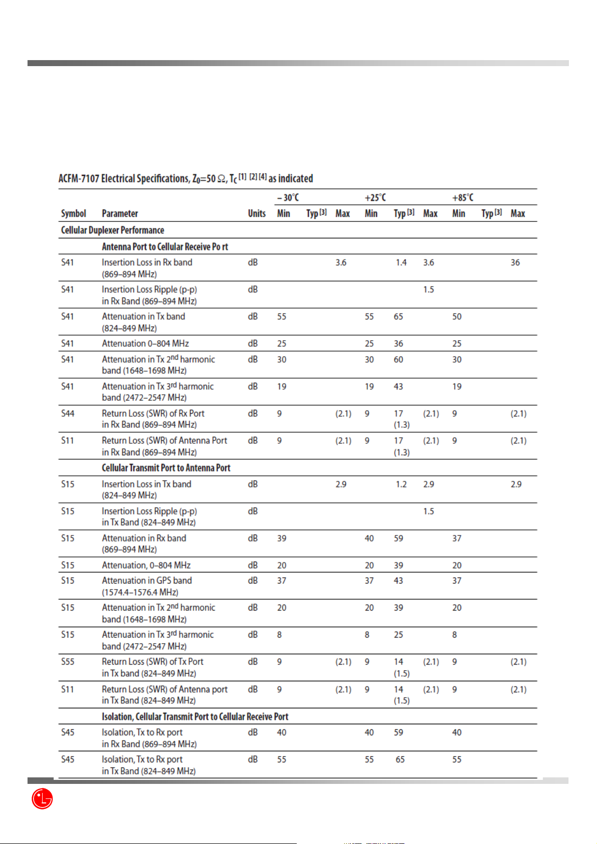
The ACFM-7107 is a quadplexer that combines US PCS and cellular duplexers into a single, miniature package.
The main function of quadplexer is to prohibit the other band signals from flowing into the one band circuit and vice
versa. The ACFM-7107 features a single antenna connection, eliminating the need for antenna switching
(800 and 1900 MHz). The specification of LN240 quadplexer is described below:
LG Electronics Inc.
23/169
LN240
LG Electronics Inc.
24/169
LN240
LG Electronics Inc.
25/169
LN240
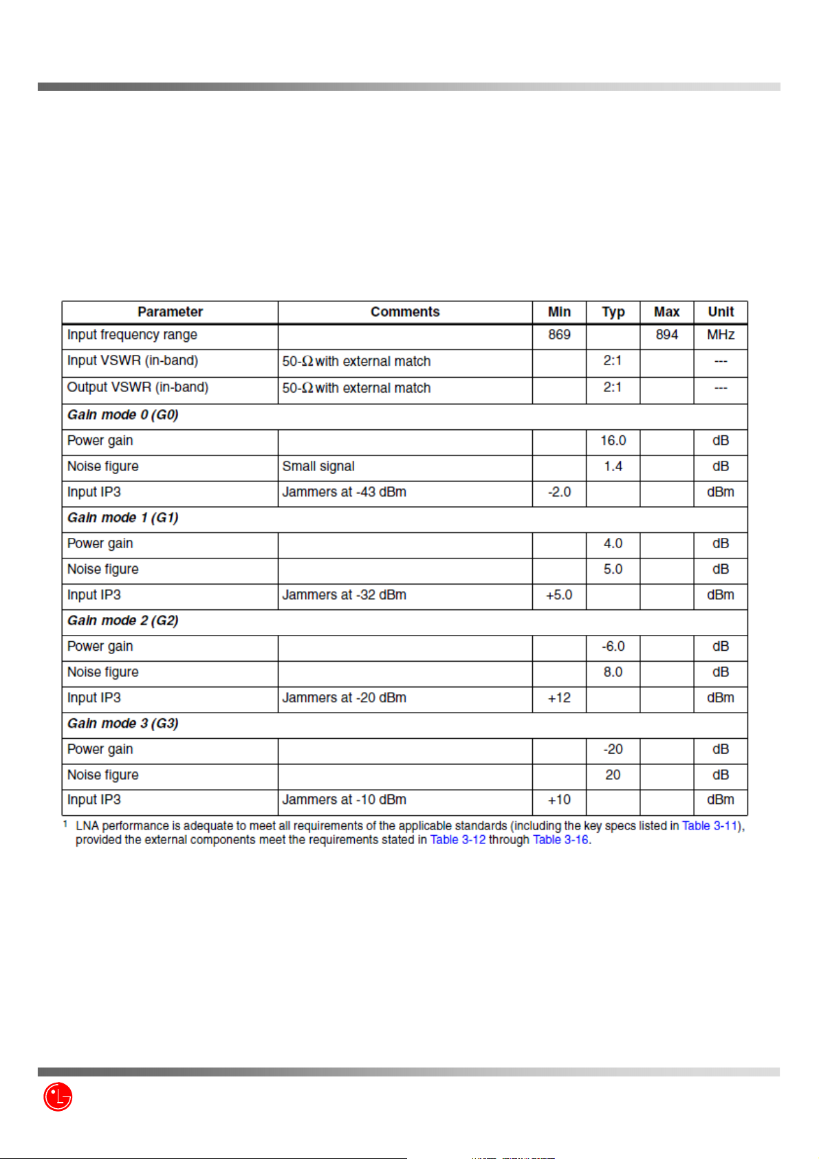
1.2.2 LNAs (U200)
The QSC6055 has cellular and PCS LNAs, respectively. The characteristics of Low Noise Amplifier ( LNA) are low
noise figure, high gain, high intercept point and high reverse isolation. The frequency selectivity characteristic of
mobile phone is mostly determined by LNA.
The specification of LG-LN240 LNAs are described below:
1.2.2.1 Cellular CDMA LNA performance specifications
LG Electronics Inc.
26/169
LN240
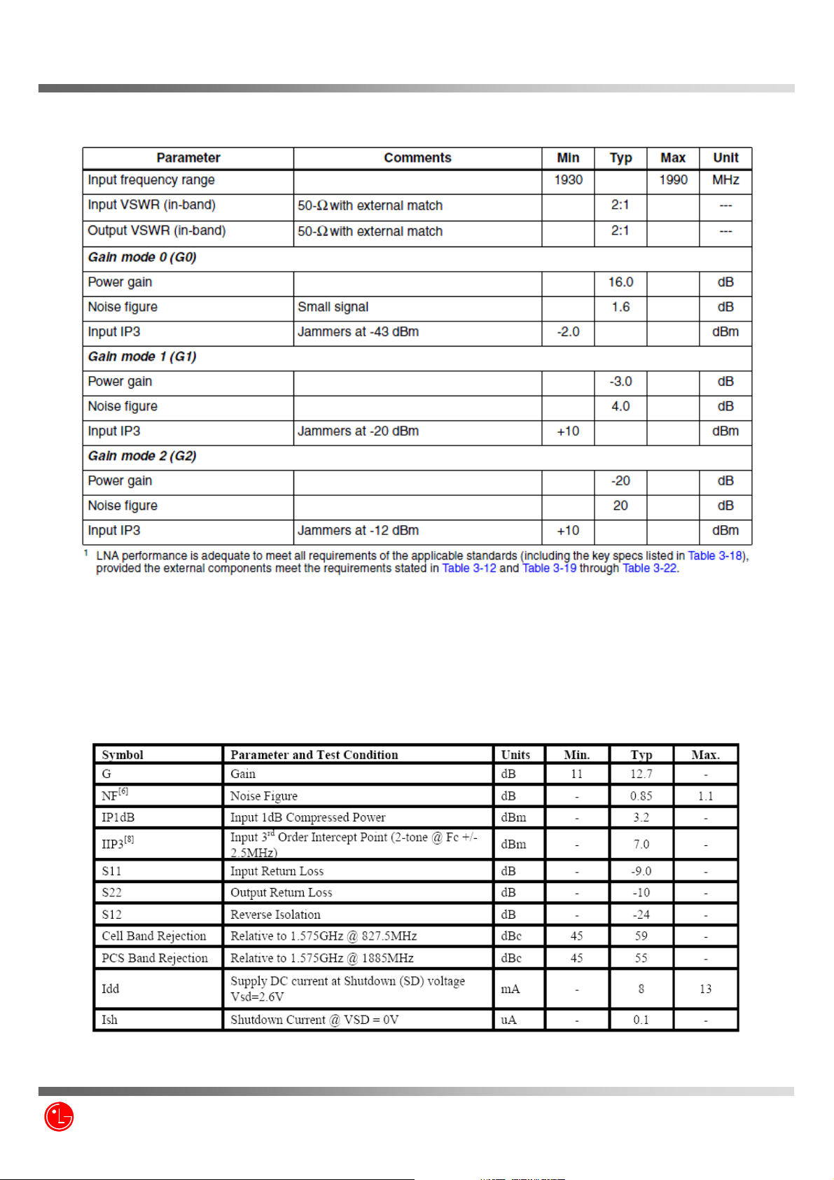
1.2.2.2 PCS CDMA LNA performance specifications
1.2.3 GPS LNA (U1302)
The characteristics of Low Noise Amplifier (LNA) are low noise figure, high gain, high intercept point and high
reverse isolation. The frequency selectivity ch aracteristic of mobile phone is mostly determined by LNA.
The specification of LG-LN240 GPS LNA is described below
LG Electronics Inc.
27/169

LN240
1.2.4 Down-converter Mixers (U200)
The QSC6055 device performs signal down-conversion for Cellular, PCS and GPS tri-band applications. It contains
all the circuitry (with the exception of external filters) needed to suppo rt conversion of received RF signals to
baseband signals. The three down-converting Mixers (Cellular, PCS and GPS), and an LO Buffer Amplifier to buffer
the RF VCO to the RF Transmit Up-converter. The GPS LNA & mixers offer the most advanced and integrated
CDMA Rx solution designed to meet cascaded Noise Figure (NF) and Third-order Intercept Point (IIP3)
requirements of IS-98C and J-STD-018 specifications for Sensitivity, Two-Tone Inter-modulation, and Single-tone
Desense.
Operation modes and band selection are specially controlled from the Qualcomm Single Chip QSC6055.
1.2.5 Rx RF SAW FILTERs(F1201, F1202,F1203)
The main function of Rx RF SAW filter is to attenuate mobile phone spurious frequency, attenuate direct RF
frequency pick up, attenuate noise at the image frequency originating in or amplified by the LNA and suppress
second harmonic originating in the LNA. The Rx RF SAW filter usually called image filter.
1.2.6 RF Receiver(U200)
The circuit functions of the RF Receive (in QSC6055) include Rx Automatic Gain Controller (AGC) with 90 dB
dynamic range, quadrature RF mixers, down-conversion mixer from RF to base-band, low pass filters and Analog to
Digital Converters (ADC) for converting to digital base-band. The RFR includes clock generators that drive the
digital processor and a VCO which generates the LO frequency for base-band down-conversion.
Switching system is located in front of the RFR RX_IN_C_LB and RX_IN_C_HB terminal and is for band selection
between cellular and PCS. The Rx AGC either amplifies or attenuates the r eceived CDMA RF signal to provide a
constant-amplitude signal to the I/Q down-converter. The RF output of the Rx AGC amplifier separate into I-channel
and Q-channel base-band components and down-converted by mixer with quadrature LO. LO signals are generated
by a Voltage Controlled Oscillator (VCO) and frequency stabilized by external varactor-tu ned resonant tank circuit.
The I/Q down converter outputs the CDMA signals at baseband frequency. Low-pass filtering enables the receiver to
select the desired baseband signals from the effects of unwanted noise or adjacent-channel interference. I/Q base
band components are converted to digital signals by two identical 4-bit ADCs.
LG Electronics Inc.
28/169
LN240
1.3 Description of Transmit Part Circuit
1.3.1 RF Transmitter (U200)
The RF Transmitter(in QSC6055, base-band-to-RF Transmit Processor) performs all Tx signal-processing functions
required between digital base-band and the Power Amplifier Module (PAM). The base-band
quadrature signals are up-converted to the Cellular or PCS frequency bands and amplified to provide signal drive
capability to the PAM. The RFT includes an RF mixer for upconverting analog baseband to RF, a programmable PLL
for generating Tx LO frequency, two cellular and two PCS driver amplifiers and Tx power control through an 85 dB
VGA. As added benefit, the single sideband upconversion eliminates the need for a band pass filter normally required
between the upconverter and driver amplifier.
I, I/, Q and Q/ signals proceed from the QSC6055 are analog signal. In CDMA mode, These signals are modulated
by Quadrature Phase Shift King (QPSK). I and Q are 90 deg. out of phase, and I and I/ are 180 deg. Tx IF signal can
be obtained by mixing analog signal with 228.6MHz (Cellular)/263.6(PCS) 1st local osillator frequency which is
generated by Tx VCO. The Tx IF signal is amplified by AGC controlled by QSC6055. The second mixer on RFT
converts IF signals into RF signals. After passing through the upconverter , RF signal is inputted into the Power
Amplifier Module.
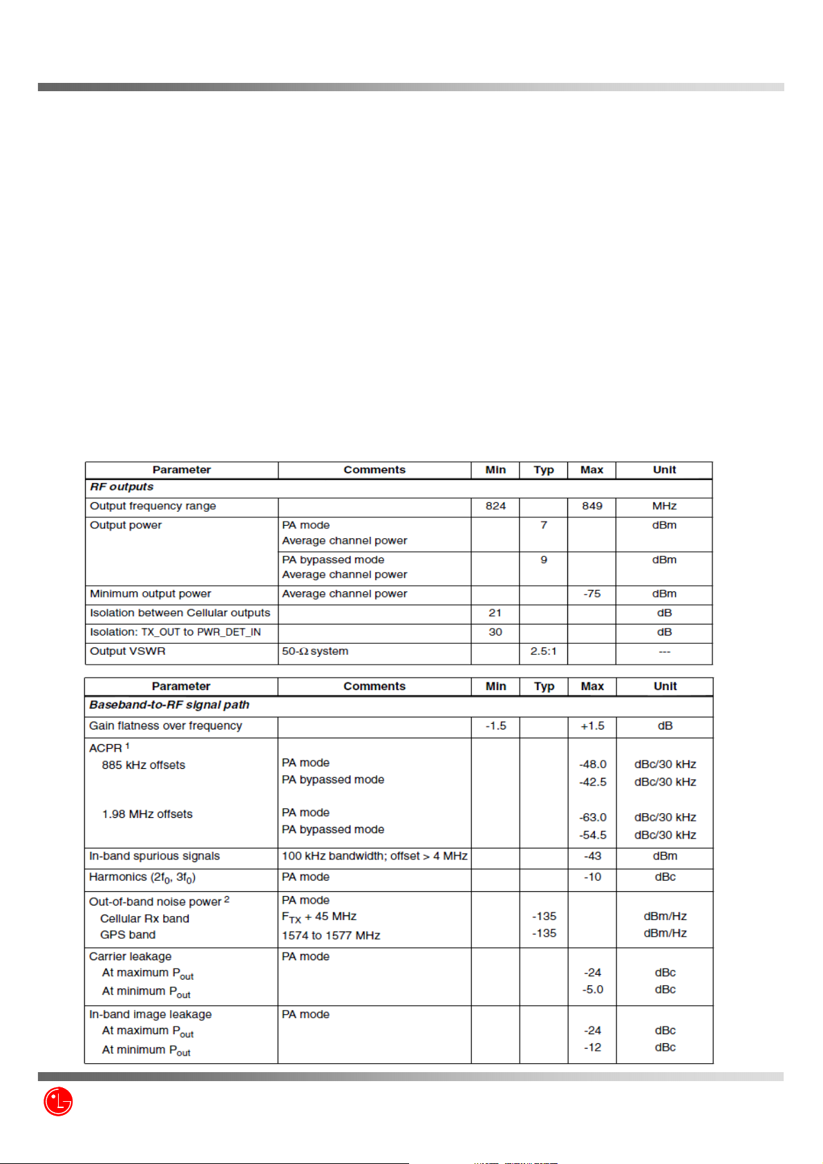
1.3.1.1 Cellular CDMA transmit signal path performance specifications
LG Electronics Inc.
29/169
LN240
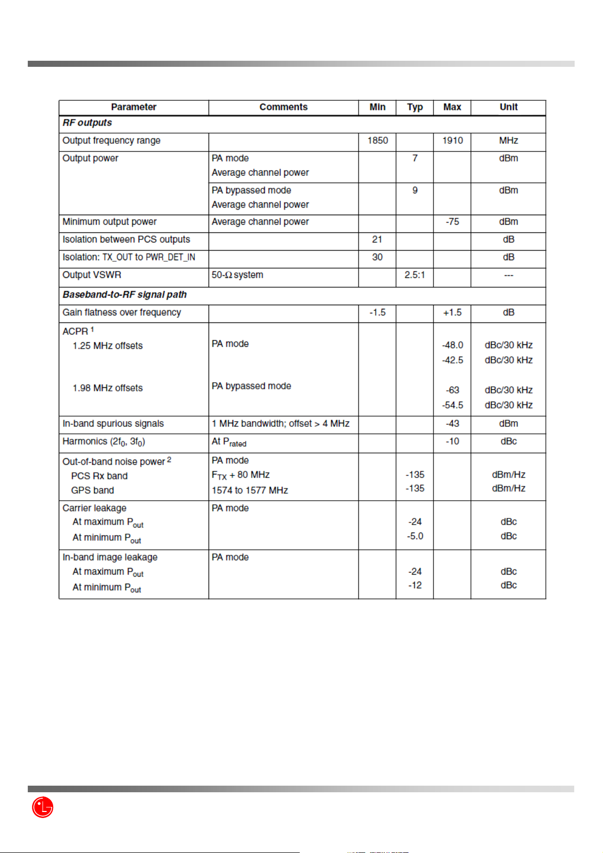
1.3.1.2 PCS CDMA transmit signal path performance specifications
1.3.2 Dual Power Amplifier(U1106 , Cellular/PCS) / AWS Power Amplifier (U1105)
The power amplifier that can be used in the PCS, Cellular and AWS mode has linear amplification capab ility and
high efficiency. For higher efficiency, it is made up of one MMIC (Monolithic Microwave Integrated Circuit) for
which RF input terminal and internal interface circuit are integrated onto one IC after going through the
AlGaAs/GaAs HBT (heterojunction bipolar transistor) process. The module of power amplifier is made up of an
output end interface circuit including this MMIC. The maximum power that can be inputted through the input
terminal is +10dBm and conversion gain is about 28dB. RF transmit signals that have been amplified through the
power amplifier are sent to the quadplexer.
LG Electronics Inc.
30/169
 Loading...