

Page 1
LCD TV
SERVICE MANUAL
CAUTION
BEFORE SERVICING THE CHASSIS,
READ THE SAFETY PRECAUTIONS IN THIS MANUAL.
CHASSIS : NF-99LA
MODEL : LN-15A10
Page 2

- 2 -
CONTENTS
Contents .................................................................................................. 2
Safety Precautions ..................................................................................3
Servicing Precautions ............................................................................ 4
Adjustment Instruction ............................................................................6
Troubleshooting .......................................................................................8
Exploded View ...................................................................................... 10
Exploded View Parts List.......................................................................11
Replacement Parts List ........................................................................ 12
SVC. Sheet .................................................................................................
Page 3
- 3 -
SAFETY PRECAUTIONS
Many electrical and mechanical parts in this chassis have special safety-related characteristics. These parts are identified by in
the Schematic Diagram and Replacement Parts List.
It is essential that these special safety parts should be replaced with the same components as recommended in this manual to
prevent X-RADIATION, Shock, Fire, or other Hazards.
Do not modify the original design without permission of manufacturer.
General Guidance
An lsolation Transformer should always be used during
the servicing of a receiver whose chassis is not isolated from
the AC power line. Use a transformer of adequate power rating
as this protects the technician from accidents resulting in
personal injury from electrical shocks.
It will also protect the receiver and it's components from being
damaged by accidental shorts of the circuitary that may be
inadvertently introduced during the service operation.
If any fuse (or Fusible Resistor) in this TV receiver is blown,
replace it with the specified.
When replacing a high wattage resistor (Oxide Metal Film
Resistor, over 1W), keep the resistor 10mm away from PCB.
Keep wires away from high voltage or high temperature parts.
Due to high vacuum and large surface area of picture tube,
extreme care should be used in handling the Picture Tube.
Do not lift the Picture tube by it's Neck.
X-RAY Radiation
Warning:
To determine the presence of high voltage, use an accurate
high impedance HV meter.
Adjust brightness, color, contrast controls to minimum.
Measure the high voltage.
The meter reading should indicate
23.5
!1.5KV: 14-19 inch, 26!1.5KV: 19-21 inch,
29.0
!1.5KV: 25-29 inch, 30.0 ! 1.5KV: 32 inch
If the meter indication is out of tolerance, immediate service
and correction is required to prevent the possibility of
premature component failure.
Before returning the receiver to the customer,
always perform an AC leakage current check on the exposed
metallic parts of the cabinet, such as antennas, terminals, etc.,
to be sure the set is safe to operate without damage of
electrical shock.
Leakage Current Cold Check(Antenna Cold Check)
With the instrument AC plug removed from AC source,
connect an electrical jumper across the two AC plug prongs.
Place the AC switch in the on positioin, connect one lead of
ohm-meter to the AC plug prongs tied together and touch other
ohm-meter lead in turn to each exposed metallic parts such as
antenna terminals, phone jacks, etc.
If the exposed metallic part has a return path to the chassis, the
measured resistance should be between 1MΩ and 5.2MΩ.
When the exposed metal has no return path to the chassis the
reading must be infinite.
An other abnormality exists that must be corrected before the
receiver is returned to the customer.
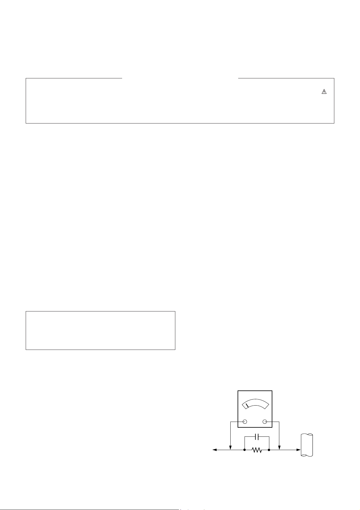
Leakage Current Hot Check (See below Figure)
Plug the AC cord directly into the AC outlet.
Do not use a line Isolation Transformer during this check.
Connect 1.5K/10watt resistor in parallel with a 0.15uF capacitor
between a known good earth ground (Water Pipe, Conduit, etc.)
and the exposed metallic parts.
Measure the AC voltage across the resistor using AC
voltmeter with 1000 ohms/volt or more sensitivity.
Reverse plug the AC cord into the AC outlet and repeat AC
voltage measurements for each esposed metallic part. Any
voltage measured must not exceed 0.75 volt RMS which is
corresponds to 0.5mA.
In case any measurement is out of the limits sepcified, there is
possibility of shock hazard and the set must be checked and
repaired before it is returned to the customer.
Leakage Current Hot Check circuit
The source of X-RAY RADIATION in this TV receiver is the
High Voltage Section and the Picture Tube.
For continued X-RAY RADIATION protection, the
replacement tube must be the same type tube as specified in
the Replacement Parts List.
IMPORTANT SAFETY NOTICE
0.15uF
AC Volt-meter
To Instrument's
exposed
METALLIC PARTS
Good Earth Ground
such as WATER PIPE,
CONDUIT etc.
1.5 Kohm/10W
Page 4

- 4 -
CAUTION: Before servicing receivers covered by this service
manual and its supplements and addenda, read and follow the
SAFETY PRECAUTIONS
on page 3 of this publication.
NOTE:
If unforeseen circumstances create conflict between the
following servicing precautions and any of the safety
precautions on page 3 of this publication, always follow the
safety precautions. Remember: Safety First.
General Servicing Precautions
1. Always unplug the receiver AC power cord from the AC
power source before;
a. Removing or reinstalling any component, circuit board
module or any other receiver assembly.
b. Disconnecting or reconnecting any receiver electrical plug
or other electrical connection.
c.
Connecting a test substitute in parallel with an electrolytic
capacitor in the receiver.
CAUTION: A wrong part substitution or incorrect
polarity installation of electrolytic capacitors may result
in an explosion hazard.
d. Discharging the picture tube anode.
2. Test high voltage only by measuring it with an appropriate
high voltage meter or other voltage measuring device (DVM,
FETVOM, etc) equipped with a suitable high voltage probe.
Do not test high voltage by "drawing an arc".
3. Discharge the picture tube anode only by (a) first connecting
one end of an insulated clip lead to the degaussing or kine
aquadag grounding system shield at the point where the
picture tube socket ground lead is connected, and then (b)
touch the other end of the insulated clip lead to the picture
tube anode button, using an insulating handle to avoid
personal contact with high voltage.
4. Do not spray chemicals on or near this receiver or any of its
assemblies.
5. Unless specified otherwise in this service manual, clean
electrical contacts only by applying the following mixture to
the contacts with a pipe cleaner, cotton-tipped stick or
comparable nonabrasive applicator; 10% (by volume)
Acetone and 90% (by volume) isopropyl alcohol (90%-99%
strength)
CAUTION: This is a flammable mixture.
Unless specified otherwise in this service manual, lubrication
of contacts in not required.
6. Do not defeat any plug/socket B+ voltage interlocks with
which receivers covered by this service manual might be
equipped.
7. Do not apply AC power to this instrument and/or any of its
electrical assemblies unless all solid-state device heat sinks
are correctly installed.
8. Always connect the test receiver ground lead to the
receiver chassis ground before connecting the test receiver
positive lead.
Always remove the test receiver ground lead last.
9.
Use with this receiver only the test fixtures specified in this
service manual.
CAUTION: Do not connect the test fixture ground strap to
any heatsink in this receiver.
Electrostatically Sensitive (ES) Devices
Some semiconductor (solid state) devices can be damaged
easily by static electricity. Such components commonly are
called
Electrostatically Sensitive (ES) Devices.
Examples of
typical ES devices are integrated circuits and some fieldeffect
transistors and semicounductor "chip" components. The
following techniques should be used to help reduce the
incidence of component damage caused by static by static
electricity.
1. Immediately before handling any semiconductor component
or semiconductor-equipped assembly, drain off any
electostatic charge on your body by touching a known earth
ground. Alternatively, obtain and wear a commercially
available discharging wrist strap device, which should be
removed to prevent potential shock reasons prior to
applying power to the unit under test.
2. After removing an electrical assembly equipped with ES
devices, place the assembly on a conductive surface such as
aluminum foil, to prevent electrostatic charge buildup or
exposure of the assembly.
3. Use only a grounded-tip soldering iron to solder or unsolder
ES devices.
4. Use only an anti-static type solder removal device. Some
solder removal devices not classified as "anti-static" can
generate electrical charges sufficent to demage ES devices.
5. Do not use freon-propelled chemicals. These can generate
electrical charges sufficient to damage ES devices.
6. Do not remove a repalcement ES device from its protective
package until immediately before you are ready to install it.
(Most replacement ES devices are packaged with leads
electrically shorted together by conductive foam, aluminum
foil or comparable conductive material).
7. Immediately before removing the protective material from
the ieads of a replacement ES device, touch the protective
material to the chassis or circuit assembly into which the
device will be installed.
CAUTION:Be sure no power is applied to the chassis or
circuit, and observe all other safety precautions.
8. Minimize bodily motions when handling unpackaged
replacement ES devices. (Otherwise harmless motion such
as the bruching together of your clothes fabric or the lifting
of your foot from a carpeted floor can generate static
electricity sufficient to damage an ES device.)
General Soldering Guidelines
1. Use a grounded-tip, low-wattage soldering iron and
appropriate tip size and shape that will maintan tip
temperature within the range or 500
cF to 600cF.
2. Use an appropriate gauge of RMA resin-core solder
composed of 60 parts tin/40 parts lead.
3. Keep the soldering iron tip clean and well tinned.
4. Thorohly clean the surfaces to be soldered. Use a mall
wirebristle (0.5 inch, or 1.25cm) brush with a metal handle.
Do not use freon-propelled spray-on cleaners.
5. Use the following unsoldering technique
a. Allow the soldering iron tip to reach normal temperature.
(500cF to 600cF)
b. Heat the component lead until the solder melts.
c. Quickly draw the melted solder with an anti-static,
suction-type solder removal device or with solder braid.
CAUTION: Work quickly to avoid overheating the
circuiboard printed foil.
6. Use the following soldering technique.
a. Allow the soldering iron tip to reach a normal
temperature (500cF to 600cF)
b. First, hold the soldering iron tip and solder the strand
against the component lead until the solder melts.
SERVICING PRECAUTIONS
Page 5

- 5 -
c. Qulckly move the soldering iron tip to the junction of the
component lead and the printed circuit foil, and hold it
there only until the solder flows onto and around both the
component lead and the foil.
CAUTION: Work quickly to avoid overheating the circuit
board printed foil.
d. Closely inspect the solder area and remove any excess
or splashed solder with a small wire-bristle brush.
IC Remove/Replacement
Some chassis circuit boards have slotted holes (oblong) through
which the IC leads are inserted and then bent flat against the
circuit foil. When holes are the slotted type, the following
technique should be used to remove and replace the IC. When
working with boards using the familiar round hole, use the
standard technique as outlined in parapraphs 5 and 6 above.
Removal
1. Desolder and straighten each IC lead in one operation by
gently prying up on the lead with the soldering iron tip as the
solder melts.
2. Draw away the melted solder with an anti-static suctiontype solder removal device (or with solder braid) before
removing the IC.
Replacement
1. Carefully insert the replacement IC in the circuit boare.
2. Carefully bend each IC lead against the circuit foil pad and
solder it.
3. Clean the soldered areas with a small wire-bristle brush.
(It is not necessary to reapply acrylic coating to the areas).
"Small-Signal" Discrete Transistor
Removal/Replacement
1. Remove the defective transistor by clipping its leads as
close as possible to the component body.
2. Bend into a "U" shape the end of each of three leads
remaining on the circuit board.
3. Bend into a "U" shape the replacement transistor leads.
4. Connect the replacement transistor leads to the
corresponding leads extending from the circuit board and
crimp the "U" with long nose pliers to insure metal to metal
contact then solder each connection.
Power Output, Transistor Device
Removal/Replacement
1. Heat and remove all solder from around the transistor leads.
2. Remove the heatsink mounting screw (if so equipped).
3. Carefully remove the transistor from the heat sink of the
circuit board.
4. Insert new transistor in the circuit board.
5. Solder each transistor lead, and clip off excess lead.
6. Replace heatsink.
Diode Removal/Replacement
1. Remove defective diode by clipping its leads as close as
possible to diode body.
2. Bend the two remaining leads perpendicula y to the circuit
board.
3. Observing diode polarity, wrap each lead of the new diode
around the corresponding lead on the circuit board.
4. Securely crimp each connection and solder it.
5. Inspect (on the circuit board copper side) the solder joints of
the two "original" leads. If they are not shiny, reheat them
and if necessary, apply additional solder.
Fuse and Conventional Resistor
Removal/Replacement
1. Clip each fuse or resistor lead at top of the circuit board
hollow stake.
2. Securely crimp the leads of replacement component around
notch at stake top.
3. Solder the connections.
CAUTION: Maintain original spacing between the replaced
component and adjacent components and the circuit board
to prevent excessive component temperatures.
Circuit Board Foil Repair
Excessive heat applied to the copper foil of any printed circuit
board will weaken the adhesive that bonds the foil to the circuit
board causing the foil to separate from or "lift-off" the board.
The following guidelines and procedures should be followed
whenever this condition is encountered.
At IC Connections
To repair a defective copper pattern at IC connections use the
following procedure to install a jumper wire on the copper
pattern side of the circuit board. (Use this technique only on IC
connections).
1. Carefully remove the damaged copper pattern with a sharp
knife. (Remove only as much copper as absolutely
necessary).
2. carefully scratch away the solder resist and acrylic coating
(if used) from the end of the remaining copper pattern.
3. Bend a small "U" in one end of a small gauge jumper wire and
carefully crimp it around the IC pin. Solder the IC connection.
4. Route the jumper wire along the path of the out-away
copper pattern and let it overlap the previously scraped end
of the good copper pattern. Solder the overlapped area and
clip off any excess jumper wire.
At Other Connections
Use the following technique to repair the defective copper
pattern at connections other than IC Pins. This technique
involoves the installation of a jumper wire on the component
side of the circuit board.
1. Remove the defective copper pattern with a sharp knife.
Remove at least 1/4 inch of copper, to ensure that a
hazardous condition will not exist if the jumper wire opens.
2. Trace along the copper pattern from both sides of the
pattern break and locate the nearest component that is
directly connected to the affected copper pattern.
3. Connect insulated 20-gauge jumper wire from the lead of
the nearest component on one side of the pattern break to
the lead of the nearest component on the other side.
Carefully crimp and solder the connections.
CAUTION: Be sure the insulated jumper wire is dressed so
the it does not touch components or sharp edges.
Page 6
- 6 -
1. Application Object
This instruction is for the application to the LCD TV.
2. Notes
(1) This set uses an adapter, so connect the adapter and the
set correctly before adjustment.
(2) The adjustment must be performed under the correct
sequence.
(3) The adjustment must be performed in the circumstance of
25!5cC of temperature and 65!10% of relative humidity if
there is no specific designation.
(4) The input voltage of the receiver must keep 220V, 60Hz in
adjusting.
(5) The set must be operated for 30 minutes preliminarily
before adjustment if there is no specific designation.
[ ‘Heat Run’ must be performed with the full white signal or TV
noise signal in the internal part of the set.
[ The time for ‘Heat Run’ can be changed owing to production
plan.
3. TV Mode Adjustment
Before entering into the adjustment mode set the TV up with
the MENU button as below.
Contrast 85
Brightness 100
Saturation 50
Tint 0
3-1. White Balance Adjustment
3-1-1. Required Test Equipment
(1) A Remote Control
(2) A Color Analyzer for LCD : CA-110
(3) A TV Signal Generator : Pattern of 64 (128) tones or Ch. 13
in the company.
3-1-2. Preparation for Adjustment
(1) This adjustment should be performed 30 minutes later
after ‘Heat Run’.
(2) This adjustment should be performed in a darkroom or in
the simmilar condition.
3-1-3. Low Light Adjustment
(1) Seletc Ch.13 in the company.
(2) Enter into the adjustment mode with the ADJ button.
(3) Select the Sub-bright and stop adjusting at the moment
when Gray 0 and 1 aren’t distinguished.
4. PC Input Mode Adjustment
4-1. Required Test Equipment
(1) A pattern generator being in proportion to VG819 ; Pattern
of 64 tones
(2) A remote control
4-2. Preparation for Adjustment
(1) Perform ‘Heat Run’ for more than 30 minutes in white
pattern.
(2) Connect the signal of pattern generator with LCD TV.
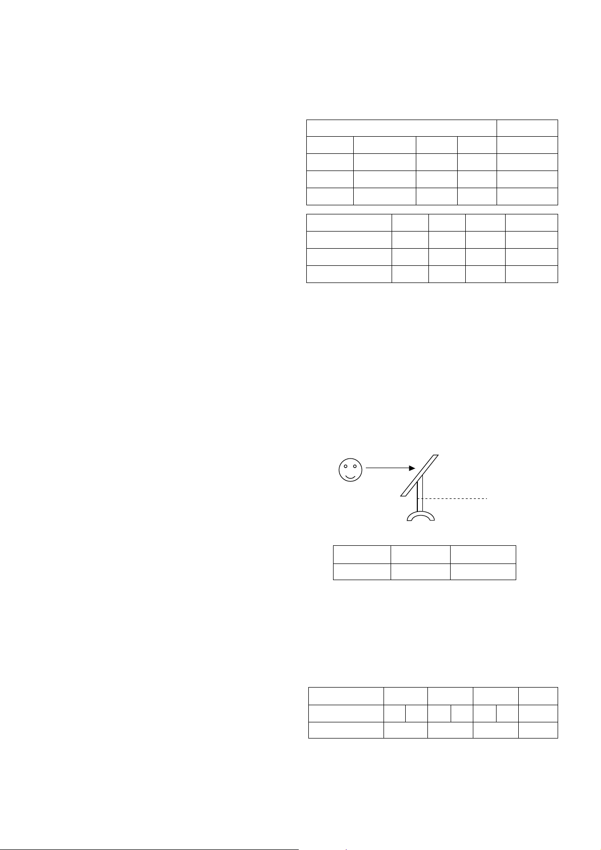
(3) Lean the set 45° backward. (Adjustment is easy.)
(4) Set the PC mode menu as below.
4-3. White Adjustment
(1) Approve the signal of 64 tones of XGA(1024 * 768).
(2) Select all the gain of R, B and G with using ADJ of remote
control.
(3) After making 62 tones, 63 tones and 64 tones not
distinguished with using each signal of R, G and B, finish
adjusting at the moment when the signal 62, 63 and 64 is
distinguished.
ADJUSTMENT INSTRUCTION
IC
VPC3230D
VPC3230D
VPC3230D
Name
BR
ACC_Sat
Tint
Default
0
2930
0
Unit-Decimal
Adj. Mode
No.304
No.236~237
No.248
IIC Type
IIC 0x52/7:0/
IIC 0x30/11:0/
Fp 0xDC
Low Light(Black)
3 x
3 y
Brightness:[cd/m^2]
Blue
0.14
0.10
Green
0.30
0.60
White
0.32
0.34
150[cd/m^2]
Red
0.63
0.34
45°
Initial Value
Contrast
70
Brightness
100
R
0.63 0.34
0x02
G
0.30 0.60
0x03
B
0.14 0.10
0x04
Error
! 0.03
Register
Color Coordinates(x,y)
AD9884
Page 7

- 7 -
4-4. Position of Mode Adjustment
Timing of Mode Table * H[dot]/V[line]
Mode
H_Total
H_Display
H_Blanking
H_Sync
H Polarity
H_Bp
H_Fp
H-Freq[KHz]
/Clk[MHz]
V_Total
V_Display
V_Blanking
V_Sync
V Polarity
V_Bp
V_Fp
VGA-60
800
640
160
96
NEG.
48
16
31.469
25.175
525
480
45
2
NEG
33
10
VGA-67
864
640
224
64
NEG.
96
64
35.0
30.24
525
480
45
3
NEG
39
3
VGA-72
832
656
176
40
NEG.
120
16
37.861
31.5
520
496
24
3
NEG
20
1
VGA-75
840
640
200
64
NEG.
120
16
37.5
31.5
500
480
20
3
NEG
16
1
VGA-85
832
640
192
56
NEG.
80
56
43.269
36.0
509
480
29
3
NEG
25
1
TEXT-70
900
720
180
108
NEG.
54
18
31.469
28.324
449
400
49
2
POS
34
13
SVGA-56
1024
800
224
72
POS
128
24
35.156
36.0
625
600
25
2
POS
22
1
SVGA-60
1056
800
256
128
POS
88
40
37.879
40.0
628
600
28
4
POS
23
1
SVGA-72
1040
800
240
120
POS
64
56
48.077
50.0
666
600
66
6
POS
23
37
Mode
H_Total
H_Display
H_Blanking
H_Sync
H Polarity
H_Bp
H_Fp
H-Freq[KHz]
/Clk[MHz]
V_Total
V_Display
V_Blanking
V_Sync
V Polarity
V_Bp
V_Fp
SVGA-75
1056
800
256
80
POS
160
16
46.875
49.5
625
600
25
3
POS
21
1
SVGA-85
1048
800
248
64
POS
152
32
53.674
56.25
631
600
31
3
POS
27
1
XGA-60
1344
1024
320
136
NEG
136
160
48.363
65.0
806
768
38
6
NEG
29
3
XGA-70
1328
1024
304
136
NEG
144
24
56.476
75.0
806
768
38
6
NEG
29
3
XGA-75
1312
1024
288
96
POS
176
16
60.23
78.75
800
768
32
3
POS
28
1
MAC-75
1152
832
320
64
NEG
224
32
49.725
57.283
667
624
43
3
NWG
39
1
Page 8

9 No sound Defective Reset IC of IC603 1) Check volume and speaker
- Speaker Defective MSP3400D of IC601 - Sound comes out only when being inputted into Audio
- Earphone L/R
2) Check after replacing IC603
3) Replace IC601
10 Video color beat noise Earphone shield case being touched
Check the mould of shield and JA401, Replace shield case
Soldering IC901 and IC501 Re-soldering
1 Soft touch doesn’t Defective speaker wire 1) Make some space between the speaker wire and
function properly and inverter wire the Soft touch Board by sticking the speaker wire
to the guide hole of the cabinet.
2) Arrange working state of A1. Tape in the inverter wire
and correct working state of the Shield case.
2 Soft touch doesn’t 1) Broken components and 1) Check Soft touch with eyes
function soldering of them Check and repair soldering
2) P101 connector error 2) Check and repair the P101 connector
3 No screen Input error of inverter connector 1) Bend the pin legs of P802 connector -> recheck them
2) Check and repair the IC806 SI4925
P501 and Pin 41 connector 1) Check and fix P501 connector
being slipped out 2) Check and fix the components at P501 LCD module
and at main board.
3) Check Pin41 and check and repair rubber packing
Cracked components and 1) Check and repair tuner board and main board
soldering at tuner board 2) Solder Q301, Q801 and R810
4 Dark screen 1) Defective LCD lamp 1) Replace the inverter
2) Defective inverter 2) Replace the LCD lamp
5 Broken OSD display Defective the font rom of IC502 Replace the font rom of IC502
- 8 -
TROUBLESHOOTING
1. General Features
2. PC Mode
No. Symptom Cause Check Point
No. Symptom Cause Check Point
Check Point
6 Screen noise Clock or phase being 1) Resettig is needed according to the video card of each
not able to be adjusted PC
2) Horizontal noise : adjust phase until no horizontal
noise occurres
3) Vertical noise : adjust clock in menu until no vertical
noise occurres
7 Screen position error Screen position error Adjust horizontal and vertical position until the screen
horizontally or vertically displayes normally
8 Color beat noise Soldering AD converter Recheck adn repair AD9884
or making it short
3. TV and external input
No. Symptom Cause
Page 9

MEMO
- 9 -
Page 10

- 10 -
EXPLODED VIEW
300
120
121
174
112
550
540
500
521
400
541
430
440
420
310
JA401
JA402
A3
410
JA701
Page 11

- 11 -
112 6304VT1512A LCD MODULE,151X2-C2TH 15.1”
120 6400VA0017A SPEAKER,GENERAL T401SX-095K14 LG C&D 8 OHM 1.0
121 4950V00010A METAL,HOLDER SPK SBHG
174 6410VUH003A POWER CORD,PS204-001 VOLEX UL/CSA 1800MM
300 3091V00226D CABINET ASSY,LN-15A10 ZENITH
310 5020V00360A BUTTON,CONTROL 8KEY ABS LN-15A1
400 3809V00168D BACK COVER ASSY
410 4950V00025A METAL,STAND ASSY
420 4950V00006A METAL,STAND SECC
430 4930V00103B HOLDER,STAND
440 3550V00081A BASE,COVER
500 6871VMM363C PCB ASSY,MAIN NF99LA US
521 4950V00009A FRAME ASSY,REAR METAL
540 6633VA0003A INVERTER ASSY,12VOLT 500VOLT
541 4814V00143B CASE,INVERTER SHIELD
550 6871VSM480A PCB ASSY,CTL NF99LA LN-15A1
A3 6634VBW002C ADAPTER,AC-DC AC110VOLT DC12VOLT UL/CSA/JAPAN
JA401 6613V00008D JACK ASSY,PMJ014D E/P(ST)+S-VH
JA402 6613V00004J JACK ASSY,PJ6054J A/V I/O 3P U
JA701 6630VGA001B CONNECTOR,68114-1522 MOLEX-KOR 15PIN
EXPLODED VIEW PARTS LIST
No.
PART NO.
DESCRIPTION
Page 12

REPLACEMENT PARTS LIST
LOCA. NO PART NO DESCRIPTION
Q708
Q709
Q711
Q712
Q713
Q714
Q715
Q720
Q721
Q722
Q723
Q725
Q726
Q727
Q728
Q801
Q900
D101
D102
D701
D702
D801
D802
D803
D804
ZD101
ZD102
ZD103
ZD104
ZD105
ZD106
ZD107
ZD108
ZD109
ZD170
ZD171
ZD172
ZD173
ZD174
ZD175
ZD176
ZD177
ZD178
ZD179
ZD180
ZD181
ZD182
0TR388009BB
0TR388009BB
0TR387500AA
0TR387500AA
0TR387500AA
0TR387500AA
0TR387500AA
0TR102009AG
0TR102009AG
0TR102009AG
0TR102009AG
0TR102009AG
0TR102009AG
0TR102009AG
0TR102009AG
0TR387500AA
0TR387500AA
0DD181009AB
0DD181009AB
0DD247109AA
0DD247109AA
0DR190309AA
0DR190309AA
0DD181009AB
0DD181009AB
0DZ511109AA
0DZ511109AA
0DZ511109AA
0DZ511109AA
0DZ511109AA
0DZ511109AA
0DZ511109AA
0DZ511109AA
0DZ511109AA
0DZ511109AA
0DZ511109AA
0DZ511109AA
0DZ511109AA
0DZ511109AA
0DZ511109AA
0DZ511109AA
0DZ511109AA
0DZ511109AA
0DZ511109AA
0DZ511109AA
0DZ511109AA
0DZ511109AA
KTC3880-Y TP KEC SOT23 CHIP
KTC3880-Y TP KEC SOT23 CHIP
CHIP 2SC3875S(ALY) KEC
CHIP 2SC3875S(ALY) KEC
CHIP 2SC3875S(ALY) KEC
CHIP 2SC3875S(ALY) KEC
CHIP 2SC3875S(ALY) KEC
CHIP KRC102S SOT-23 TP KEC
CHIP KRC102S SOT-23 TP KEC
CHIP KRC102S SOT-23 TP KEC
CHIP KRC102S SOT-23 TP KEC
CHIP KRC102S SOT-23 TP KEC
CHIP KRC102S SOT-23 TP KEC
CHIP KRC102S SOT-23 TP KEC
CHIP KRC102S SOT-23 TP KEC
CHIP 2SC3875S(ALY) KEC
CHIP 2SC3875S(ALY) KEC
SWITCHING,CHIP KDS181 85V 300MA KEC
SWITCHING,CHIP KDS181 85V 300MA KEC
DETECTOR,1S2471
DETECTOR,1S2471
RECTIFIER,MBRS190T3 TP MOTOROLA 403A-0
RECTIFIER,MBRS190T3 TP MOTOROLA 403A-0
SWITCHING,CHIP KDS181 85V 300MA KEC
SWITCHING,CHIP KDS181 85V 300MA KEC
ZENER,DTZ5.1BTT11(CHIP) TP ROHM
ZENER,DTZ5.1BTT11(CHIP) TP ROHM
ZENER,DTZ5.1BTT11(CHIP) TP ROHM
ZENER,DTZ5.1BTT11(CHIP) TP ROHM
ZENER,DTZ5.1BTT11(CHIP) TP ROHM
ZENER,DTZ5.1BTT11(CHIP) TP ROHM
ZENER,DTZ5.1BTT11(CHIP) TP ROHM
ZENER,DTZ5.1BTT11(CHIP) TP ROHM
ZENER,DTZ5.1BTT11(CHIP) TP ROHM
ZENER,DTZ5.1BTT11(CHIP) TP ROHM
ZENER,DTZ5.1BTT11(CHIP) TP ROHM
ZENER,DTZ5.1BTT11(CHIP) TP ROHM
ZENER,DTZ5.1BTT11(CHIP) TP ROHM
ZENER,DTZ5.1BTT11(CHIP) TP ROHM
ZENER,DTZ5.1BTT11(CHIP) TP ROHM
ZENER,DTZ5.1BTT11(CHIP) TP ROHM
ZENER,DTZ5.1BTT11(CHIP) TP ROHM
ZENER,DTZ5.1BTT11(CHIP) TP ROHM
ZENER,DTZ5.1BTT11(CHIP) TP ROHM
ZENER,DTZ5.1BTT11(CHIP) TP ROHM
ZENER,DTZ5.1BTT11(CHIP) TP ROHM
ZENER,DTZ5.1BTT11(CHIP) TP ROHM
LOCA. NO PART NO DESCRIPTION
IC101
IC102
IC104
IC105
IC301
IC401
IC402
IC501
IC502
IC601
IC602
IC603
IC604
IC605
IC606
IC607
IC608
IC701
IC702
IC801
IC808
IC901
IC503
IC802
IC803
IC804
IC805
IC806
IC807
Q100
Q101
Q102
Q301
Q302
Q303
Q304
Q501
Q601
Q602
Q702
Q703
Q704
Q705
Q706
Q707
0IZZVC0007E
0IKE704200J
0IAL241600B
0IPH740800F
0IKE780900N
0IAD988400A
0ISH323422A
0IAR300000A
0IZZVA0007G
0IIT344000B
0IKE780800J
0IKE704200J
0IPH705200C
0IPH705200C
0ISH092100A
0ISH092100A
0IKE780500Q
0ISG747410A
0ISG747410A
0ITC786000A
0IKE780500Q
0IIT323000A
0TF492509AA
0TF993609AA
0TF941009AA
0TF993609AA
0TF941009AA
0TF492509AA
0TF492509AA
0TR387500AA
0TR387500AA
0TR387500AA
0TR387500AA
0TR387500AA
0TR387500AA
0TR150400BA
0TR387500AA
0TR387500AA
0TR387500AA
0TR388009BB
0TR388009BB
0TR388009BB
0TR388009BB
0TR388009BB
0TR388009BB
M37274EASP 52S DIP 52 BK US
KIA7042AF SOT-89 TP 4.2V VOLTA
AT24C16-10PC 8D EEPROM 16K
74HC08D SO-14 TP QUAD 2-INPUT
KIA7809AP 3 ST REGULATOR .
AD9884 100P MQFP BK A/D CONVER
PQ3RF23 4P(TO-220) 3.3V REGUL
AL300 160P PQFP BK LCD MONITOR
M27C512 28 BK US
MSP3440G QA 80QFP TP AUDIO MUL
KIA7808API 3P ST REGULATOR
KIA7042AF SOT-89 TP 4.2V VOLTA
TDA7052A 8P,DIP BK 1W AUDIO AM
TDA7052A 8P,DIP BK 1W AUDIO AM
PQ09RF21 4P 9V S/W REGULATOR
PQ09RF21 4P 9V S/W REGULATOR
KIA7805API 3P TO-220 ST REGULATOR 5V
M74HC74M1R 14P,SOP TP DUAL DTY
M74HC74M1R 14P,SOP TP DUAL DTY
SI786 28SSOP TP DUAL-OUTPUT PO
KIA7805API 3P TO-220 ST REGULATOR 5V
VPC3230D 80P PQFP BK COMB FILT
FET,SI4925DY TP TEMIC 30V 6.1A SO
FET,SI9936DY TP TEMIC 30V 5A SO-8
FET,SI9410DY TP TEMIC 30V 7A SO-8
FET,SI9936DY TP TEMIC 30V 5A SO-8
FET,SI9410DY TP TEMIC 30V 7A SO-8
FET,SI4925DY TP TEMIC 30V 6.1A SO
FET,SI4925DY TP TEMIC 30V 6.1A SO
CHIP 2SC3875S(ALY) KEC
CHIP 2SC3875S(ALY) KEC
CHIP 2SC3875S(ALY) KEC
CHIP 2SC3875S(ALY) KEC
CHIP 2SC3875S(ALY) KEC
CHIP 2SC3875S(ALY) KEC
CHIP 2SA1504S(ASY) KEC
CHIP 2SC3875S(ALY) KEC
CHIP 2SC3875S(ALY) KEC
CHIP 2SC3875S(ALY) KEC
KTC3880-Y TP KEC SOT23 CHIP
KTC3880-Y TP KEC SOT23 CHIP
KTC3880-Y TP KEC SOT23 CHIP
KTC3880-Y TP KEC SOT23 CHIP
KTC3880-Y TP KEC SOT23 CHIP
KTC3880-Y TP KEC SOT23 CHIP
IC
TRANSISTOR
- 12 -
RUN DATE : 2000.5.23
DIODE
Page 13

- 13 -
LOCA. NO PART NO DESCRIPTION
ZD183
ZD184
ZD301
ZD700
C102
C114
C115
C175
C176
C177
C178
C301
C302
C304
C308
C310
C312
C314
C320
C405
C527
C601
C602
C603
C605
C606
C608
C609
C612
C615
C625
C631
C632
C635
C637
C641
C642
C650
C801
C802
C804
C807
C809
C810
C811
C812
C813
C814
C817
C820
0DZ511109AA
0DZ511109AA
0DZ330009DF
0DZ511109AA
0CE1053K618
0CE1053K616
0CE4763F618
0CE1063F618
0CE1063F618
0CE1063F618
0CE4753K618
0CE4763F618
0CE4763F618
0CE227DF618
0CE227DF618
0CE106DK618
0CE1074F618
0CE227DF618
0CE1063F618
0CE477DF618
0CE687DD618
0CE4763F618
0CE4763F618
0CE1063F618
0CE1063F618
0CE3353K618
0CE4743K618
0CE4743K618
0CE1063F618
0CE1063F618
0CE4763F618
0CE1074F618
0CE1074F618
181-007H
181-007H
181-007H
181-007H
0CE4763F618
0CE1074F618
0CE1074F618
0CE4753K618
0CE4753K618
0CE1074F618
0CE227DF618
0CE687DD618
0CE227DF618
0CE1074F618
0CE476DK618
0CE227DF618
0CE337DF618
ZENER,DTZ5.1BTT11(CHIP) TP ROHM
ZENER,DTZ5.1BTT11(CHIP) TP ROHM
ZENER,MTZJ33B TP ROHM-K DO34 0.5W 33
ZENER,DTZ5.1BTT11(CHIP) TP ROHM
1UF SRE 50V M
1UF SRE 50V M
47UF SRE 16V M
10UF SRE 16V M
10UF SRE 16V M
10UF SRE 16V M
4.7UF SRE 50V M
47UF SRE 16V M
47UF SRE 16V M
220UF STD 16V M
220UF STD 16V M
10UF STD 50V M
100UF SRA 16V M
220UF STD 16V M
10UF SRE 16V M
470UF STD 16V M
680UF STD 10V M
47UF SRE 16V M
47UF SRE 16V M
10UF SRE 16V M
10UF SRE 16V M
3.3UF SRE 50V M
0.4700UF SRE 50V M
0.4700UF SRE 50V M
10UF SRE 16V M
10UF SRE 16V M
47UF SRE 16V M
100UF SRA 16V M
100UF SRA 16V M
MPE ECQ-V1H474JL3(TR), 50V 0.4
MPE ECQ-V1H474JL3(TR), 50V 0.4
MPE ECQ-V1H474JL3(TR), 50V 0.4
MPE ECQ-V1H474JL3(TR), 50V 0.4
47UF SRE 16V M
100UF SRA 16V M
100UF SRA 16V M
4.7UF SRE 50V M
4.7UF SRE 50V M
100UF SRA 16V M
220UF STD 16V M
680UF STD 10V M
220UF STD 16V M
100UF SRA 16V M
47UF STD 50V M
220UF STD 16V M
330UF STD 16V M
LOCA. NO PART NO DESCRIPTION
C823
C908
C910
C912
C943
C944
C945
C946
F801
JA401
JA402
JA801
L300
L301
L302
L401
L402
L403
L501
L502
L503
L504
L505
L506
L507
L508
L601
L602
L603
L801
L804
L806
L900
L901
LA501
LA502
LA503
LA504
LA505
LA506
L101
L701
L802
L803
L805
L902
0CE1074F618
0CE1063F618
0CE1063F618
0CE1063F618
0CE1053K616
0CE1053K616
0CE1053K616
0CE1053K616
131-096K
6613V00008D
6613V00004J
6612VAH001B
6210TCE001G
6210TCE001G
6210TCE001G
6210TCE001G
6210TCE001G
6210TCE001E
6210TCE001G
6210TCE001E
6210TCE001E
6210TCE001A
6210TCE001E
6210TCE001G
6210TCE001E
6210TCE001E
6210TCE001G
6210TCE001G
6210TCE001G
6210TCE001G
6210TCE001G
6210TCE001G
6210TCE001G
6210TCE001G
6210TCE002A
6210TCE002A
6210TCE002A
6210TCE002A
6210TCE002A
6210TCE002A
0LA0152K119
0LA0222K119
6140VB0004A
6140VB0004B
6140VB0004B
0LA0152K119
100UF SRA 16V M
10UF SRE 16V M
10UF SRE 16V M
10UF SRE 16V M
1UF SRE 50V M
1UF SRE 50V M
1UF SRE 50V M
1UF SRE 50V M
FUSE,NON TIME DELAY 135% 2,000MA 125V
JACK ASSY,PMJ014D E/P(ST)+S-VH
JACK ASSY,PJ6054J A/V I/O 3P U
JACK,AC/DC POWER HEC3900-010110
CORE(CIRC),BEAD HH-1M3216-501
CORE(CIRC),BEAD HH-1M3216-501
CORE(CIRC),BEAD HH-1M3216-501
CORE(CIRC),BEAD HH-1M3216-501
CORE(CIRC),BEAD HH-1M3216-501
CORE(CIRC),BEAD HB-1M2012-800JT
CORE(CIRC),BEAD HH-1M3216-501
CORE(CIRC),BEAD HB-1M2012-800JT
CORE(CIRC),BEAD HB-1M2012-800JT
CORE(CIRC),BEAD HB-1S2012-080JT
CORE(CIRC),BEAD HB-1M2012-800JT
CORE(CIRC),BEAD HH-1M3216-501
CORE(CIRC),BEAD HB-1M2012-800JT
CORE(CIRC),BEAD HB-1M2012-800JT
CORE(CIRC),BEAD HH-1M3216-501
CORE(CIRC),BEAD HH-1M3216-501
CORE(CIRC),BEAD HH-1M3216-501
CORE(CIRC),BEAD HH-1M3216-501
CORE(CIRC),BEAD HH-1M3216-501
CORE(CIRC),BEAD HH-1M3216-501
CORE(CIRC),BEAD HH-1M3216-501
CORE(CIRC),BEAD HH-1M3216-501
CORE(CIRC),BEAD HB-4M3216-800JT
CORE(CIRC),BEAD HB-4M3216-800JT
CORE(CIRC),BEAD HB-4M3216-800JT
CORE(CIRC),BEAD HB-4M3216-800JT
CORE(CIRC),BEAD HB-4M3216-800JT
CORE(CIRC),BEAD HB-4M3216-800JT
INDUCTOR,15UH K
INDUCTOR,22UH K
COIL,CHOKE 9.5UH 1UEWPHY 13.5TURN YL-9N
COIL,CHOKE 26UH 1UEWPHY 22.5TURN YL-9N
COIL,CHOKE 26UH 1UEWPHY 22.5TURN YL-9N
INDUCTOR,15UH K
FUSE & JACK
CORE
CAPACITOR
COIL & TRANSFORMER
For Capacitor & Resistors, the
charactors at 2nd and 3rd digit
in the P/No. means as follows;
CC, CX, CK, CN : Ceramic
CQ : Polyestor
CE : Electrolytic
RD : Carbon Film
RS : Metal Oxide Film
RN : Metal Film
RF : Fusible
Page 14

- 14 -
LOCA. NO PART NO DESCRIPTION
L903
T801
R321
R605
R607
R617
R618
RA501
RA503
RA505
RA507
RA509
RA511
X101
X601
X901
JA701
LD1
PA001
SP701
TU301
X501
A1
A2
A3
0LA0152K119
6170VTCA30A
0RS0561K607
0RD1200H609
0RD1200H609
0RS0681K607
0RS0681K607
0RRZVTA001A
0RRZVTA001A
0RRZVTA001A
0RRZVTA001A
0RRZVTA001A
0RRZVTA001A
156-A01P
156-A02M
6202VDB007B
6630VGA001B
0DL112100AB
6726VV0006D
6908VB0001A
6700VNF003E
6204V00001J
3828VA0131F
6710V00044T
6634VBW002C
INDUCTOR,15UH K
TRANSFORMER,CONVERTER[COIL] EPC 13-Z 320UH
5.60 2W 5%
120 1/2W 5%
120 1/2W 5%
6.80 2W 5%
6.80 2W 5%
MNR-14-E0A-J-101 R OHM 100 OH
MNR-14-E0A-J-101 R OHM 100 OH
MNR-14-E0A-J-101 R OHM 100 OH
MNR-14-E0A-J-101 R OHM 100 OH
MNR-14-E0A-J-101 R OHM 100 OH
MNR-14-E0A-J-101 R OHM 100 OH
CRYSTAL,HC49U RADIAL 8.000MHZ 30
CRYSTAL,HC49U RADIAL 18.432MHZ 30P
CRYSTAL,HC49U RADIAL 20.250MHZ 3
CONNECTOR,68114-1522 MOLEX-KOR 15PIN
LED,DL-11S2GN1 OPTO
PRE-AMP,TSOP4838ON1 TEMIC 38.0KHZ HOLD
BUZZER,PKM13EPY-4002 MURATA 4000HZ 70
TUNER,TAUG-H006P LG PRECISION CO., L
OSCILLATOR,OSC-SCO060 RADIAL 14.318
MANUAL,OWNERS NF99LA LN-15A10 ZENITH EN
REMOTE CONTROLLER,NF99LA LN-15A10
ADAPTER,AC-DC AC110VOLT DC12VOLT UL/CSA/J
LOCA. NO PART NO DESCRIPTION
MISCELLANEOUS
ACCESSORIES
RESISTOR
CRYSTAL
For Capacitor & Resistors, the
charactors at 2nd and 3rd digit
in the P/No. means as follows;
CC, CX, CK, CN : Ceramic
CQ : Polyestor
CE : Electrolytic
RD : Carbon Film
RS : Metal Oxide Film
RN : Metal Film
RF : Fusible
Page 15

- 12 -
June, 2000
P/NO : 3828VD0066S Printed in Korea
Page 16

PRINTED CIRCUIT BOARD
MAIN(TOP)
CTL(TOP)
CTL(BOTTOM)
TUNER(TOP)
TUNER(BOTTOM)
MAIN(BOTTOM)
BLOCK DIAGRAM
Tuner & IF
- 6700VNF003C
Audio
Processor
- MSP3400C
Ext- L
Micro-Controller
- M 37274
Audio-Amp
TDA7052A
L
LCD
< 6-bits >
Video
Decorder
- VPC3230D
Video Scaler
- AL300
Computer
Signal
- D-Sub
R/G/B
H/V
D-R/G/B,
H / V -Sync,
Den, Clock
From
Computer
EPROM
For OSD
CVBS
Audio-Amp
TDA7052A
R
Ext- R
SIF
For MNT Application
LM151X2
1H/1V
A to D Converter
- AD9884
For MNT Application
For PC Input
- Contrast
- Brightness
- Color
Ext_Video
Ext_Y/C
OSD FB/R/G/B
DVD Y/Pb/Pr
For TV
. Contrast
. Brightness
. Color
. Tint
CVBS For Caption
Page 17

VIDEO
AUDIO
Y
C
 Loading...