

Page 1
- 1-1 -
[CONTENTS]
❍ SECTION 1.GENERAL
• SERVICING PRECAUTIONS . . . . . . . . . . . . . . . . . . . . . . . . . . . . . . . . . . . . . . . . . . . . . . . 1-2
• ESD PRECAUTIONS . . . . . . . . . . . . . . . . . . . . . . . . . . . . . . . . . . . . . . . . . . . . . . . . . . . . . 1-4
❍ SECTION 2.ELECTRICAL SECTION
• TROUBLESHOOTING GUIDE . . . . . . . . . . . . . . . . . . . . . . . . . . . . . . . . . . . . . . . . . . . . . . 2-1
• INTERNAL BLOCK DIAGRAM of ICs . . . . . . . . . . . . . . . . . . . . . . . . . . . . . . . . . . . . . . . . . 2-21
• BLOCK DIAGRAM . . . . . . . . . . . . . . . . . . . . . . . . . . . . . . . . . . . . . . . . . . . . . . . . . . . . . . . 2-25
• SCHEMATIC DIAGRAMS . . . . . . . . . . . . . . . . . . . . . . . . . . . . . . . . . . . . . . . . . . . . . . . . . 2-27
• WIRING DIAGRAM . . . . . . . . . . . . . . . . . . . . . . . . . . . . . . . . . . . . . . . . . . . . . . . . . . . . . . 2-39
• PRINTED CIRCUIT BOARD DIAGRAM . . . . . . . . . . . . . . . . . . . . . . . . . . . . . . . . . . . . . . . 2-41
❍ SECTION 3. EXPLODED VIEWS . . . . . . . . . . . . . . . . . . . . . . . . . . . . . . . . . . . 3-1
❍ SECTION 4. SPEAKER PART . . . . . . . . . . . . . . . . . . . . . . . . . . . . . . . . . . . . . 4-1
❍ SECTION 5. REPLACEMENT PARTS . . . . . . . . . . . . . . . . . . . . . . . . . . . . . . . 5-1
Page 2
- 1-2 -
SECTION 1. GENERAL
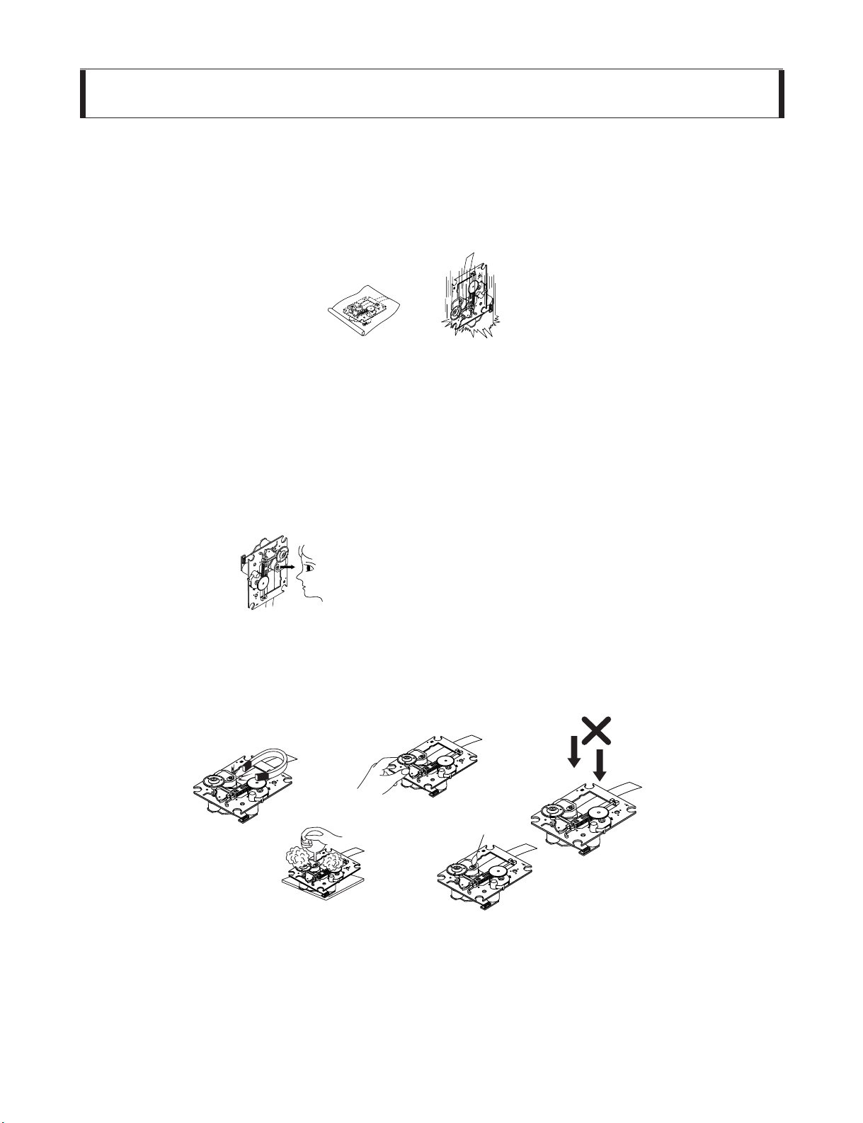
❏ SERVICING PRECAUTIONS
NOTES REGARDING HANDLING OF THE PICK-UP
1. Notes for transport and storage
1) The pick-up should always be left in its conductive bag until immediately prior to use.
2) The pick-up should never be subjected to external pressure or impact.
2. Repair notes
1) The pick-up incorporates a strong magnet, and so should never be brought close to magnetic materials.
2) The pick-up should always be handled correctly and carefully, taking care to avoid external pressure and
impact. If it is subjected to strong pressure or impact, the result may be an operational malfunction and/or
damage to the printed-circuit board.
3) Each and every pick-up is already individually adjusted to a high degree of precision, and for that reason
the adjustment point and installation screws should absolutely never be touched.
4) Laser beams may damage the eyes!
Absolutely never permit laser beams to enter the eyes!
Also NEVER switch ON the power to the laser output part (lens, etc.) of the pick-up if it is damaged.
5) Cleaning the lens surface
If there is dust on the lens surface, the dust should be cleaned away by using an air bush (such as used
for camera lens). The lens is held by a delicate spring. When cleaning the lens surface, therefore, a cotton
swab should be used, taking care not to distort this.
6) Never attempt to disassemble the pick-up.
Spring by excess pressure. If the lens is extremely dirty, apply isopropyl alcohol to the cotton swab. (Do
not use any other liquid cleaners, because they will damage the lens.) Take care not to use too much of
this alcohol on the swab, and do not allow the alcohol to get inside the pick-up.
Storage in conductive bag
Drop impact
NEVER look directly at the laser beam, and don’t let
contact fingers or other exposed skin.
Magnet
How to hold the pick-up
Conductive Sheet
Cotton swab
Pressure
Pressure
Page 3

- 1-3 -
NOTES REGARDING COMPACT DISC PLAYER REPAIRS
1. Preparations
1) Compact disc players incorporate a great many ICs as well as the pick-up (laser diode). These components
are sensitive to, and easily affected by, static electricity. If such static electricity is high voltage, components
can be damaged, and for that reason components should be handled with care.
2) The pick-up is composed of many optical components and other high-precision components. Care must be
taken, therefore, to avoid repair or storage where the temperature of humidity is high, where strong magnetism is present, or where there is excessive dust.
2. Notes for repair
1) Before replacing a component part, first disconnect the power supply lead wire from the unit
2) All equipment, measuring instruments and tools must be grounded.
3) The workbench should be covered with a conductive sheet and grounded.
When removing the laser pick-up from its conductive bag, do not place the pick-up on the bag. (This is
because there is the possibility of damage by static electricity.)
4) To prevent AC leakage, the metal part of the soldering iron should be grounded.
5) Workers should be grounded by an armband (1M Ω)
6) Care should be taken not to permit the laser pick-up to come in contact with clothing, in order to prevent static electricity changes in the clothing to escape from the armband.
7) The laser beam from the pick-up should NEVER be directly facing the eyes or bare skin.
CLEARING MALFUNCTION
You can reset your unit to initial status if malfunction occur(button malfunction, display, etc.).
Using a pointed good conductor(such as driver), simply short the RESET jump wire on the inside of
the volume knob for more than 3 seconds.
If you reset your unit, you must reenter all its settings(stations, clock, timer)
NOTE: 1.To operate the RESET jump wire, pull the volume rotary knob and release it.
2. If you wish to operate the RESET jump wire, it is necessary to unplug the power cord.
Resistor
(1 Mohm)
Conductive
Sheet
Resistor
(1 Mohm)
Armband
RESET jump wire
VOLUME
VOLUME KNOB
DOWN
UP
Page 4
- 1-4 -
❏ ESD PRECAUTIONS
Electrostatically Sensitive Devices (ESD)
Some semiconductor (solid state) devices can be damaged easily by static electricity. Such components
commonly are called Electrostatically Sensitive Devices (ESD). Examples of typical ESD devices are integrated
circuits and some field-effect transistors and semiconductor chip components.The following techniques should
be used to help reduce the incidence of component damage caused by static electricity.
1. Immediately before handling any semiconductor component or semiconductor-equipped assembly, drain off
any electrostatic charge on your body by touching a known earth ground. Alternatively, obtain and wear a
commercially available discharging wrist strap device, which should be removed for potential shock reasons
prior to applying power to the unit under test.
2. After removing an electrical assembly equipped with ESD devices, place the assembly on a conductive sur-
face such as aluminum foil, to prevent electrostatic charge buildup or exposure of the assembly.
3. Use only a grounded-tip soldering iron to solder or unsolder ESD devices.
4. Use only an anti-static solder removal device. Some solder removal devices not classified as "anti-static" can
generate electrical charges sufficient to damage ESD devices.
5. Do not use freon-propelled chemicals. These can generate electrical charges sufficient to damage ESD
devices.
6. Do not remove a replacement ESD device from its protective package until immediately before you are
ready to install it. (Most replacement ESD devices are packaged with leads electrically shorted together by
conductive foam, aluminum foil or comparable conductive materials).
7. Immediately before removing the protective material from the leads of a replacement ESD device, touch the
protective material to the chassis or circuit assembly into which the device will by installed.
CAUTION : BE SURE NO POWER IS APPLIED TO THE CHASSIS OR CIRCUIT, AND OBSERVE ALL
OTHER SAFETY PRECAUTIONS.
8. Minimize bodily motions when handing unpackaged replacement ESD devices. (Otherwise harmless motion
such as the brushing together of your clothes fabric or the lifting of your foot from a carpeted floor can generate static electricity sufficient to damage an ESD device).
CAUTION. GRAPHIC SYMBOLS
THE LIGHTNING FLASH WITH APROWHEAD SYMBOL. WITHIN AN EQUILATERAL TRIANGLE, IS
INTENDED TO ALERT THE SERVICE PERSONNEL TO THE PRESENCE OF UNINSULATED “DANGEROUS VOLTAGE” THAT MAY BE OF SUFFICIENT MAGNITUDE TO CONSTITUTE A RISK OF
ELECTRIC SHOCK.
THE EXCLAMATION POINT WITHIN AN EQUILATERAL TRIANGLE IS INTENDED TO ALERT THE
SERVICE PERSONNEL TO THE PRESENCE OF IMPORTANT SAFETY INFORMATION IN SERVICE
LITERATURE.
Page 5
- 2-1 -
SECTION 2. ELECTRICAL
■ CD PART
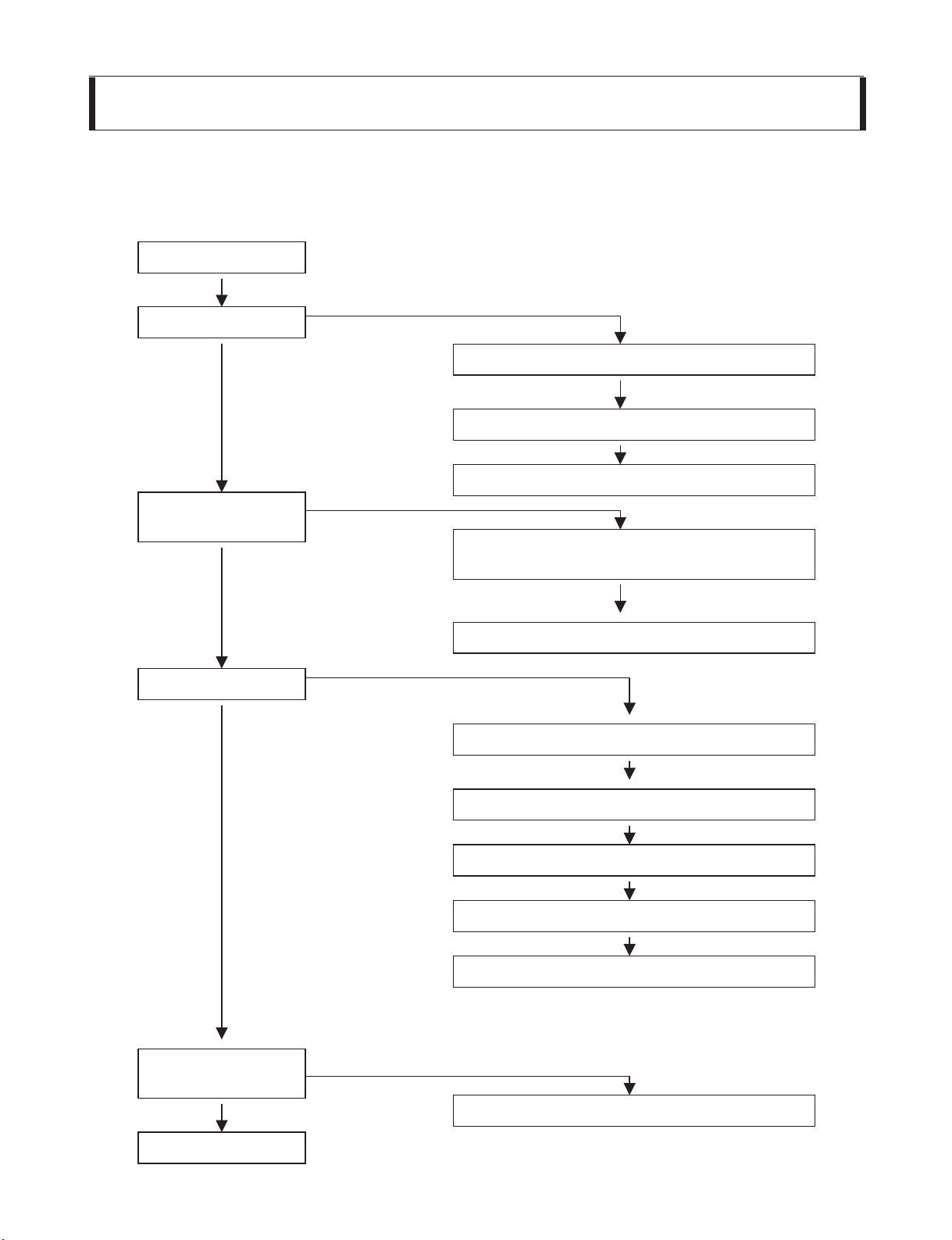
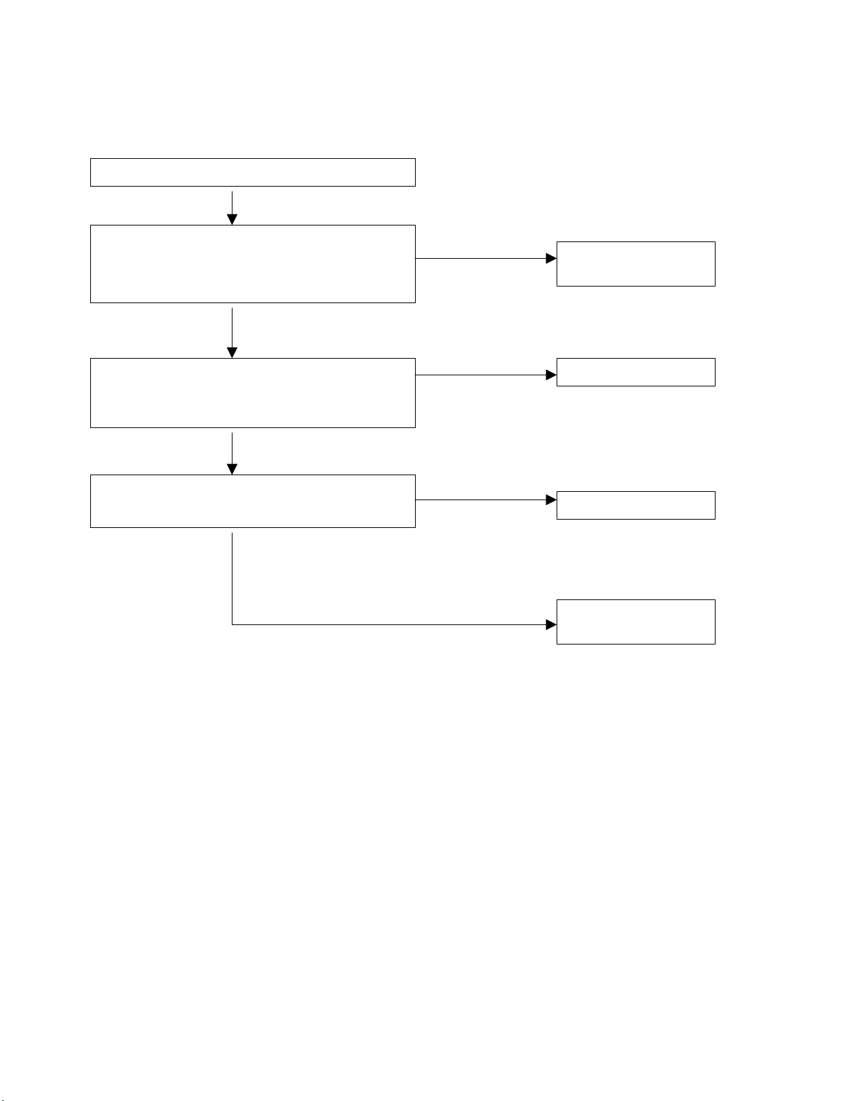
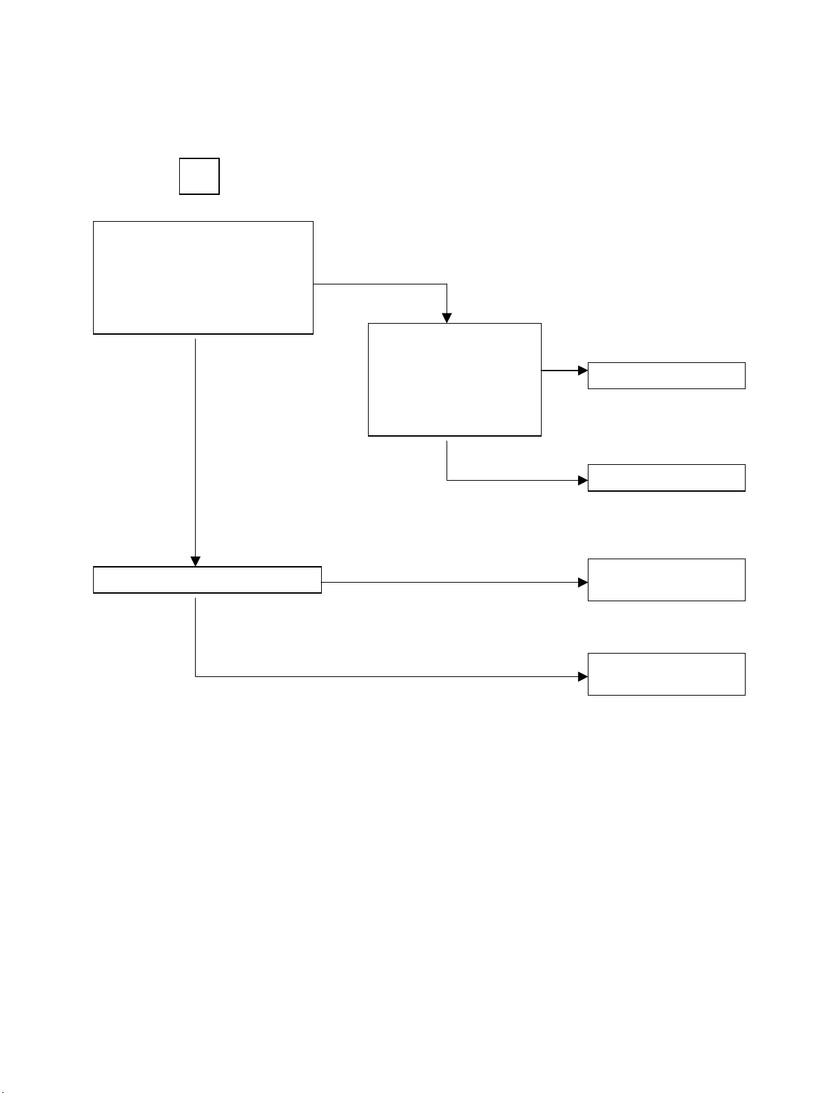
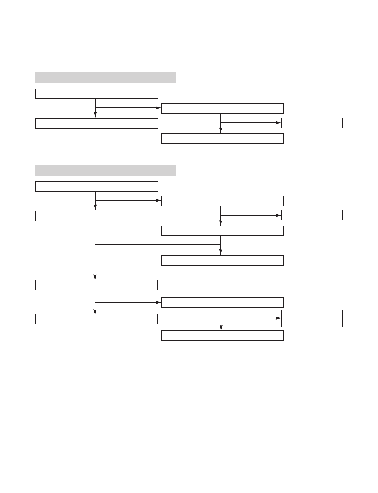
❏ TROUBLESHOOTING GUIDE
TURN ON CD
CONNECTOR CHECK ( PN808,PN807 )
CHECK POWER SUPPLY CIRCUIT( PN808 )
CHECK MICOM INTERFACE CIRCUIT( PN807 )
CHECK MICOM INTERFACE CIRCUIT( PN807 )
CONNECTOR CHECK(PN801,PN802)
CHECK PICKUP MOVEMENT
CHECK BA5810FP (IC803)
CHECK MN6627933CG (IC801)
CHECK AN22004 (IC802)
CONNECTOR CHECK (PN808)
CONNECTOR CHECK
( PN808,PN807,PN802,PN801 )
OPEN CLOSE CHECK
“ READING ”
DISPLAY CHECK
READING OK CHECK
IF PLAY, AUDIO
OUTPUT CHECK
OK
NO
NO
NO
NO
YES
YES
YES
YES
YES
Page 6
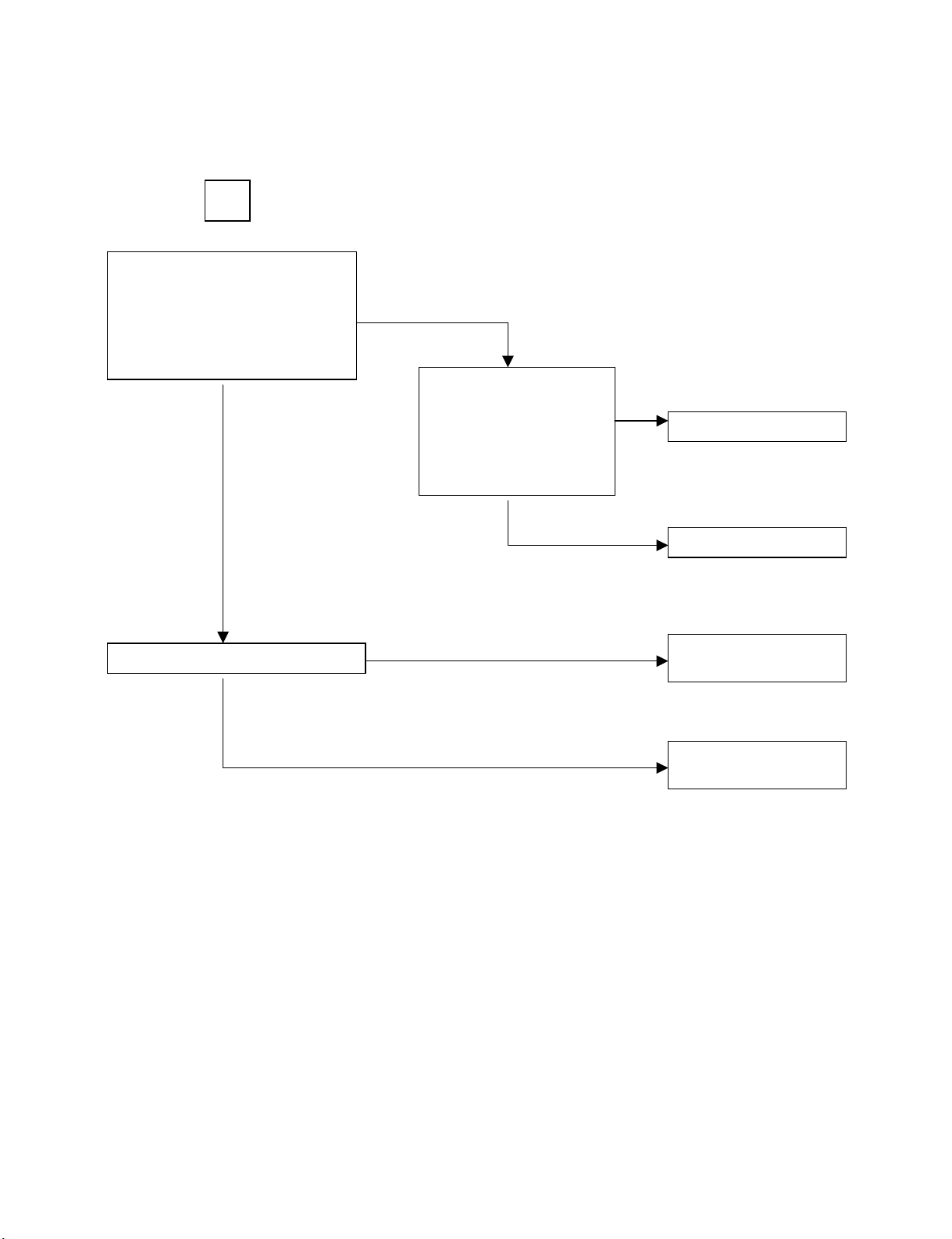
- 2-2 -
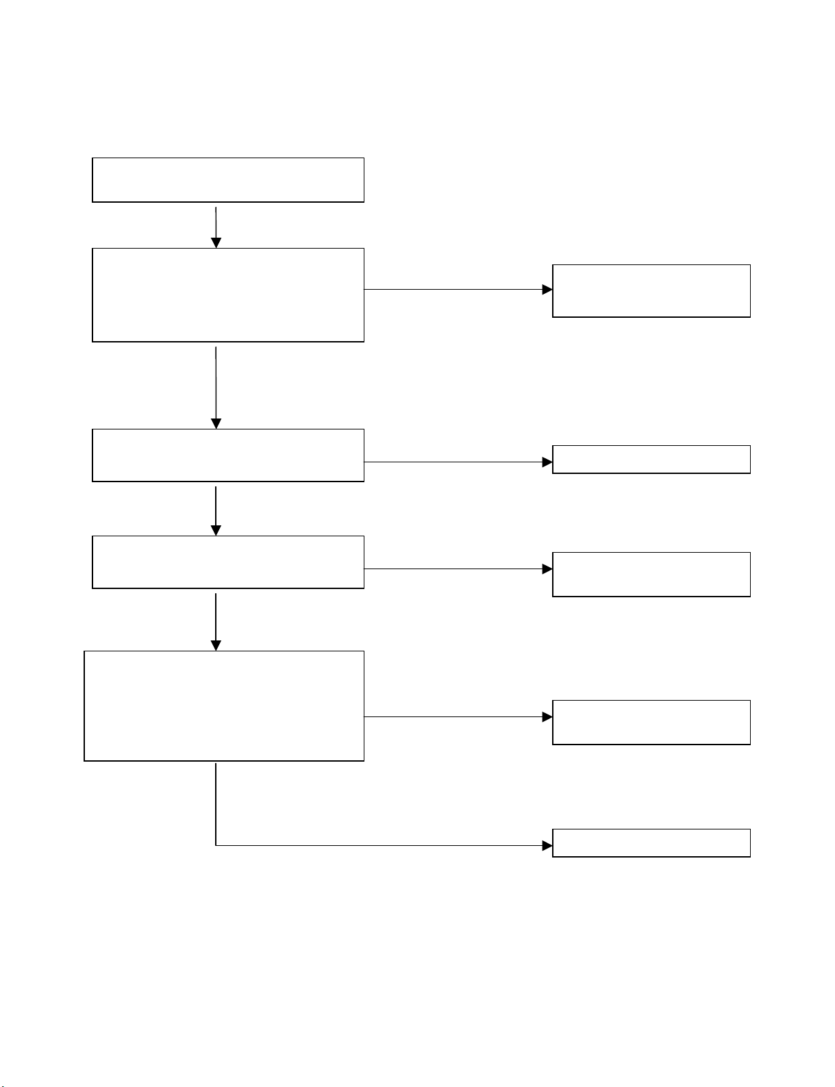
CONNECTOR LOCKING CHECK ( PN808,PN807 )
DEFECTIVE MAIN
POEWR SUPPLY
DEFECTIVE MICOM
DEFECTIVE IC803
DEFECTIVE
MECHANISM
CHECK POWER SUPPLY CIRCUIT( PN808 ,PN807)
PN808 PIN 5 = 6.2V, PIN 7 = 5V
PN807 PIN 1 = 5V
CHECK VOLTAGE CHANGE OF OPEN CLOSE ,
AND BTLMUTE VOLTAGE(= 5V)
(PN807 PIN 20:OPEN, 19:CLOSE, 4:BTLMUTE)
CHECK VOLTAGE CHANGE LO+, LO- OF IC803
(PN807, PIN OPEN:20, CLOSE:19)
YES
YES
YES
NO
NO
NO
NO
• OPEN CLOSE NG
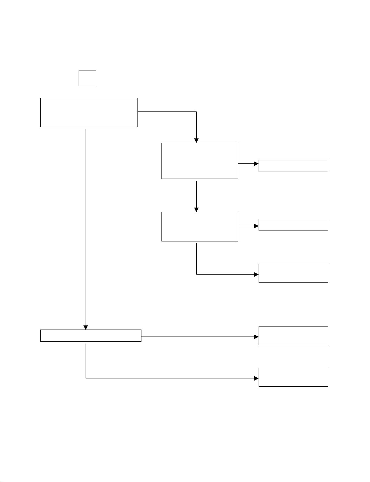
Page 7
- 2-3 -
CONNECTOR LOCKING CHECK
(PN808,PN807,PN802,PN801 )
DEFECTIVE CONNECTOR OR
MAIN POWER SUPPLAY
DEFECTIVE IC805
DEFECTIVE MICOM OR
CONNECTOR
DEFECTIVE MICOM OR
CONNECTOR
DEFECTIVE IC801
CHECK VOLTAGE THE PIN 2 OF IC805
IC805 PIN2 : 3.3V
CHECK RESET SIGNAL OF PN807
PN807 PIN12 : 5V
CHECK POWER SUPPLY
PORT( PN808 ,PN807)
PN808 PIN 5 = 6.2V, PIN 7 = 5V
PN807 PIN 1 = 5V
CHECK POWER SUPPLY
PORT( PN808 ,PN807)
PN808 PIN 5 = 6.2V, PIN 7 = 5V
PN807 PIN 1 = 5V
CHECK MICOM INTERFACE
CIRCUIT( PN807 )
PN807 PIN 11,13,14,15 SIGNAL CHECK
(11: STAT, 13: MDATA, 14:MCLK, 15:MLD)
CHECK THE WAVE FORM #1
YES
YES
YES
YES
YES
NO
NO
NO
NO
NO
• “ READING ” DISPLAY CHECK (= ONLY “CD “DISPLAY)
Page 8
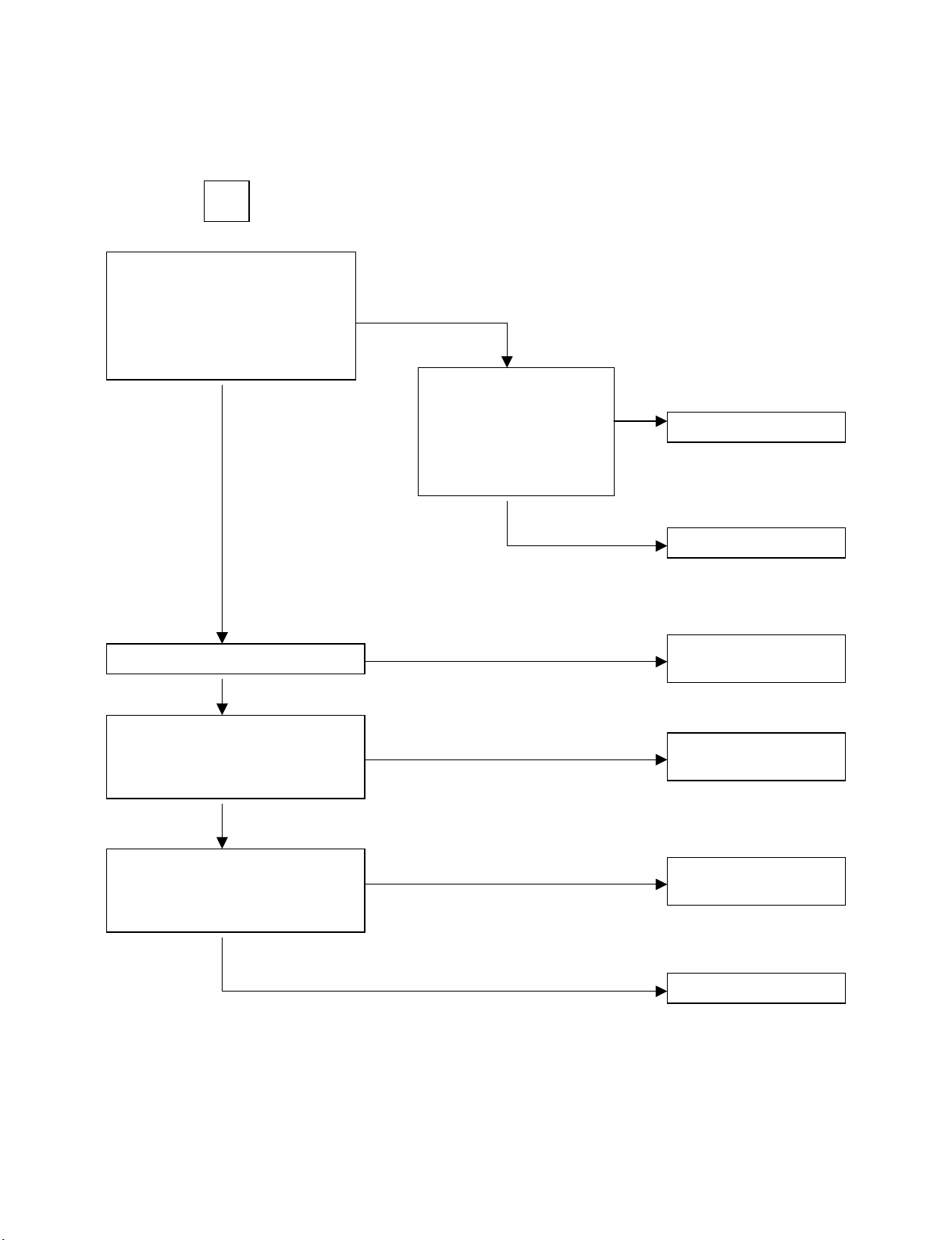
- 2-4 -
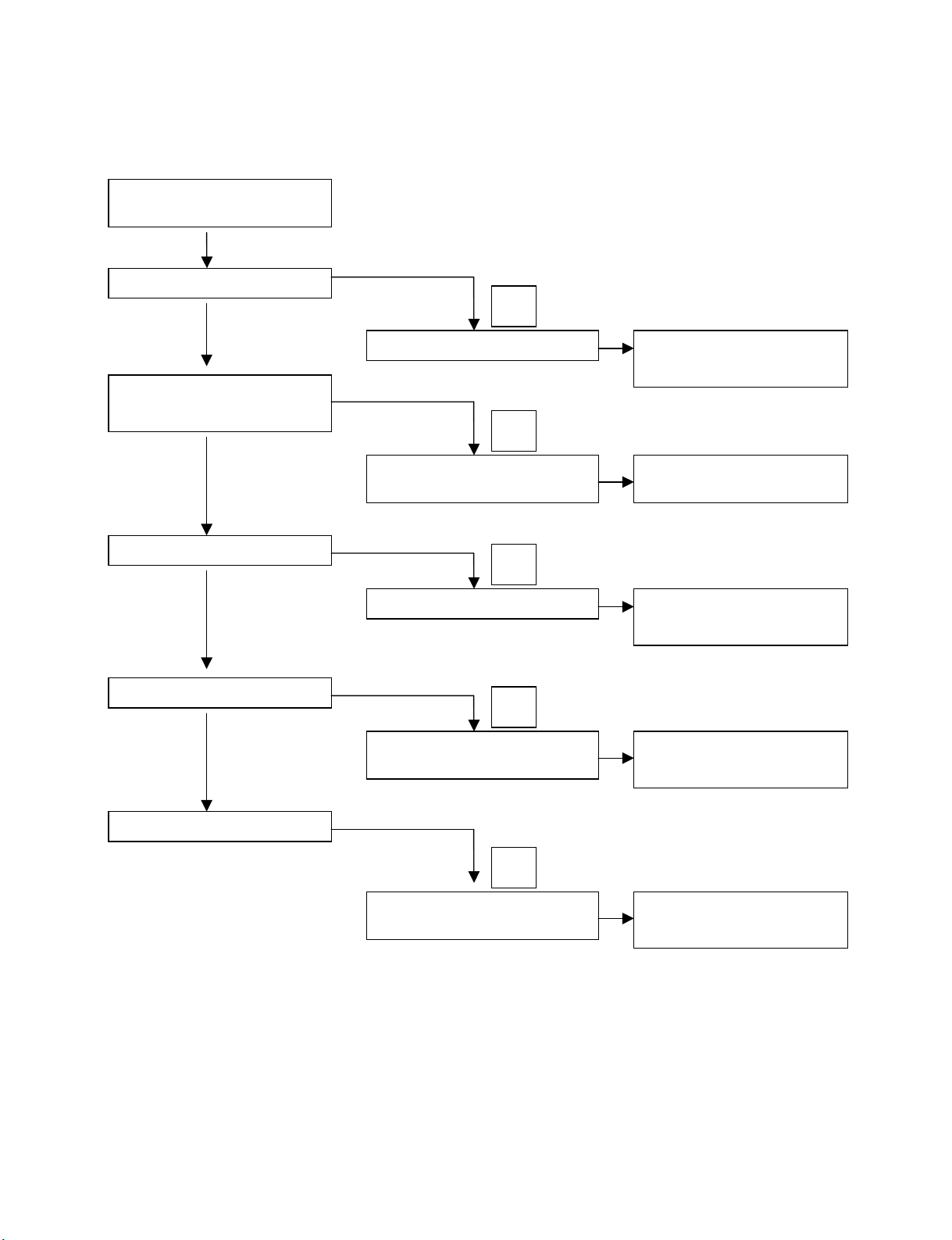
A
B
C
D
E
CONNECTOR LOCKING
CHECK(PN801,PN802)
DOES SLED MOVE ?
CHECK PN802 PIN 3,4( SL+,SL-)
DEFECTIVE PICKUP OR
IC803 OR IC801 OR IC802
DEFECTIVE PICKUP OR
IC803 OR IC801 OR IC802
DEFECTIVE PICKUP OR
IC803 OR IC801
DEFECTIVE PICKUP OR
IC802
DEFECTIVE PICKUP OR
IC803
DEFECTIVE PICKUP OR
IC803 OR IC801 OR IC802
CHECK PN802 PIN 10( LD )
CHECK PN801 PIN 14,15
(TA- ,TA+)
CHECK PN802 PIN
5,6( SP+,SP-)
CHECK PN801 PIN 13,16
( FA-, FA+)
DOES LENSE MOVE ?
(= UP & DOWN)
DOES LASER LIGHT ?
DOES SPINDLE ROTATE ?
IS READING OK ?
YES
YES
YES
YES
YES
NO
NO
NO
NO
NO
• READING OK CHECK (= “NO DISC” DISPLAY)
Page 9
- 2-5 -
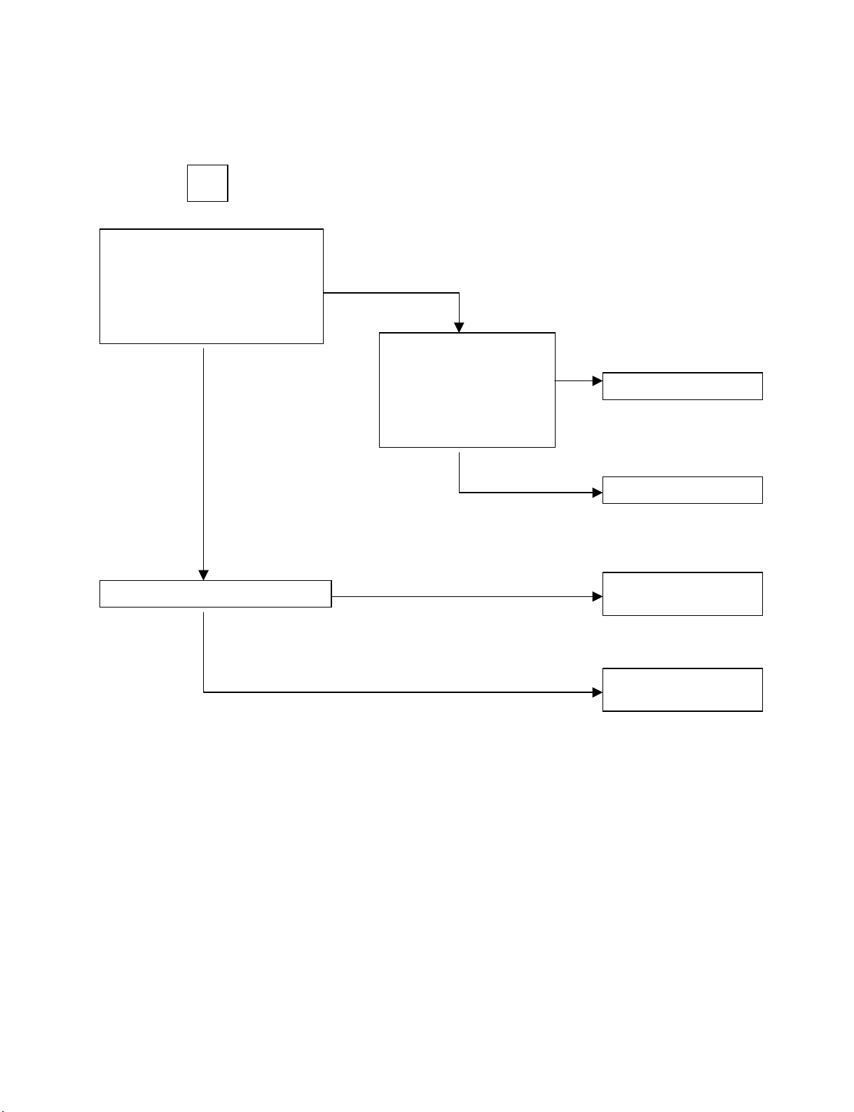
CHECK PN802 CONNECTOR LINE
DEFECTIVE IC801
DEFECTIVE IC803
DEFECTIVE PN802
CONNECTOR
DEFECTIVE PICKUP
SLED MOTOR
A
DOES SL+ WAVEFORM APPEAR AT
( IC803 PIN14 AND PN802 PIN3)
WAVEFORM #2
SLED MOTOR WAVE
DOES SLIN WAVEFORM
APPEAR AT
( IC803 PIN 5)
WAVEFORM #2
SLED DRIVE WAVE
YES
YES
NO
NO
NO
NO
NO
• READING OK CHECK #A (= “NO DISC” DISPLAY)
Page 10
- 2-6 -
CHECK PN801 CONNECTOR LINE
DEFECTIVE IC801
DEFECTIVE IC803
DEFECTIVE PN801
CONNECTOR
DEFECTIVE PICKUP
FOCUS ACTUATOR
B
DOES FA+ WAVEFORM APPEAR AT
( IC803 PIN15 AND PN801 PIN16)
WAVEFORM #3
FOCUS COIL DRIVE WAVE
DOES FAIN- WAVEFORM
APPEAR AT
( IC803 PIN 26)
WAVEFORM #3
FOCUS DRIVE WAVE
YES
YES
NO
NO
NO
NO
NO
• READING OK CHECK #B (= “NO DISC” DISPLAY)
Page 11
- 2-7 -
CHECK PN801 CONNECTOR LINE
DEFECTIVE IC805
DEFECTIVE IC802
DEFECTIVE Q801 OR
D811
DEFECTIVE PN801
CONNECTOR
DEFECTIVE PICKUP
LASER PART
C
IS ?V APPLIED TO PIN10 OF
PN801
LASER SUPPLY VOLTAGE CHECK
IS 3.3 V APPLIED TO
PIN3 OF IC802
RF IC SUPPLY VOLTAGE
CHECK
IS 2.0 V PIN2 OF IC802
LASER CONTROL
VOLTAGE CHECK
YES
YES
NO
NO
NO
NO
NO
NO
• READING OK CHECK #C (= “NO DISC” DISPLAY)
Page 12
- 2-8 -
CHECK PN802 CONNECTOR LINE
DEFECTIVE IC801
DEFECTIVE IC803
DEFECTIVE PN802
CONNECTOR
DEFECTIVE PICKUP
SPINDLE MOTOR
D
DOES SP+ WAVEFORM APPEAR AT
( IC803 PIN12 AND PN802
PIN6)WAVEFORM #4
SPINDLE MOTOR DRIVE WAVE
DOES SPIN WAVEFORM
APPEAR AT( IC803 PIN 6)
WAVEFORM #4
SPINDLE DRIVE WAVE
YES
YES
NO
NO
NO
NO
• READING OK CHECK #D (= “NO DISC” DISPLAY)
Page 13
- 2-9 -
CHECK PN802 CONNECTOR LINE
DOES ARF SIGNAL APPEAR?
(IC802 PORT 8)
WAVEFORM #6
DOES FE, TE SIGNAL APPEAR?
(IC802 PORT FE:23, TE:21)
WAVEFORM #6
DEFECTIVE IC801
DEFECTIVE IC803
DEFECTIVE PN802
CONNECTOR
DEFECTIVE PICKUP OR
IC802
DEFECTIVE PICKUP OR
IC802
DEFECTIVE IC801
E
DOES TA+ WAVEFORM APPEAR AT
( IC803 PIN17 AND PN801 PIN15)
WAVEFORM #5
TRACKING COIL DRIVE WAVE
DOES TAIN- WAVEFORM
APPEAR AT
( IC803 PIN 23)
WAVEFORM #5
TRACKING DRIVE WAVE
YES
YES
YES
NO
NO
NO
NO
NO
NO
NO
• READING OK CHECK #E (= “NO DISC” DISPLAY)
Page 14
- 2-10 -
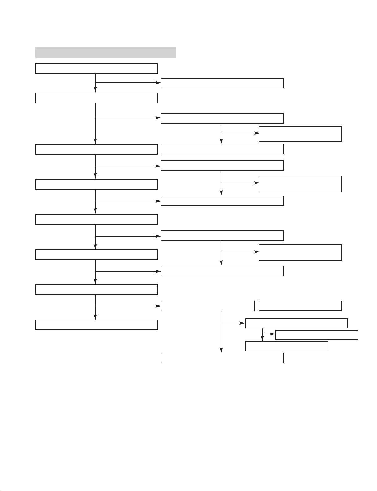
■ AUDIO PART
P-SENS PART CHECK
ZD 701(+) Voltage check
IC301 26PIN PATTERN Check
Half-wave rectification wave form check
R746 check, then ZD701 replacement
D713 Replacement
VKK CHECK
CN305 4pin DC -33V check
IC301 51PIN check
ZD 700 -33V check
ZD 754 turn on check
Pattern disconnection check
D707, D708 replacement
normal
ZD700 replacement
Refer to power
supply check
C763 -33V and less check
Q754 replacement
Page 15
- 2-11 -
POWER CHECK
Every kinds of Fuse check
C720(+), C770(-) DC power output check
C725(+), C729(-) DC power output check
IC704, IC705, IC705 power output check
IC704, IC705, IC710 power output check (12V)
IC709 DC5V check
CN513 7PIN 5V check (at CD Function)
normal operation
Fuse replace
CN704 1, 2, 3, 4, 5, 6, 7, 9, 10 AC voltage output check
D713(PBU604) check
Power supply Ass’y check
and transformer replacent
IC301 5V Power output
PN304/CN304 15 PIN check
Check
IC5019BU2090 check & replace
IC501(BU2090) 14PIN HIGH check
Check and replace defective
Power supply Ass’y check
and transformer replacent
CN704, 11, 12 pin AC power output check
IC704, IC705 , IC710 check and replacement
IC301 78PIN 5V check
IC709 replacement
Q904(A1273) Base Low check
Q904, CD Ass’y check replacement
Page 16
- 2-12 -
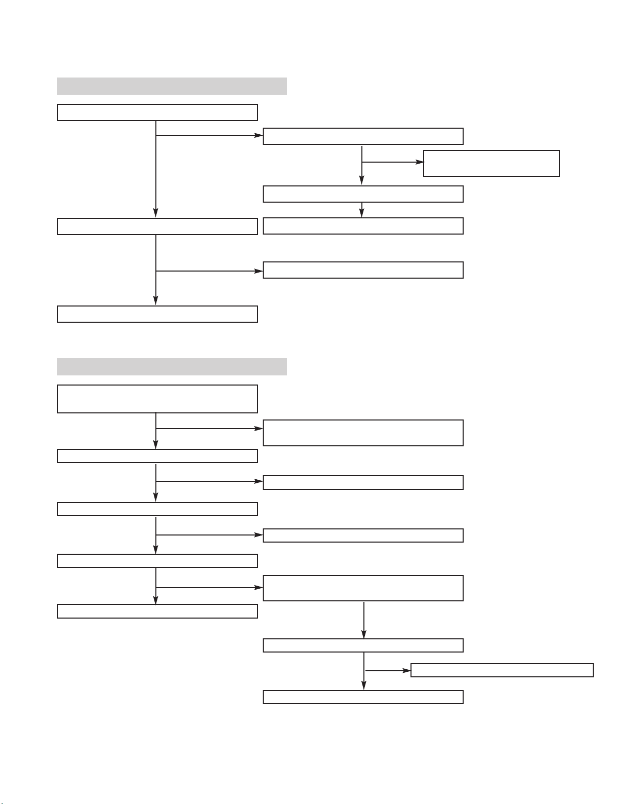
Muting circuit Troubleshooting (if MUTE)
Q752(A102) Base “LOW”
C720(+), C770(-) DC power output check
MUTE
c-COM operation status check
Each appropriate TR replacement
Check each function input and operation
status check
Refer to IC601(TDA7429D) IC specification
c-COM check (and CLK/DATA check)
IC705 7812 operation status check (DC12V)
PN701/CN701 connection status check
ZD601 9.1V check
IC601 39PIN (over 8V) check and power
supply circuit check
Q702(A102) operation status check
Q702(A102) Replace if defective
c-COM 2PIN(A-MUTE)
LINE check
No sound
Input check (AUX➞29,36 TUNER➞30,35
TAPE➞28/37 CD➞31/34 PIN)
IC 601 24/25 PIN Output check
IC601 input check (22/21PIN)
IC601 output check (14PIN)
normal
Page 17

- 2-13 -
Refer to IC202 Troubleshooting
IC501 10 PIN(PB MUTE) operation status check
c-COM 301 10,8 PIN CLK/DATA operation status check
Specific FUNCTION MODE has no sound (TDA7468D)
TAPE
IC202 output check (5,20 PIN)
IC601 36,29 PIN signal input check
IC202 input check (HEAD input) "A"DECK
1,24 "B"DECK 23,2
AUX
JK102 signal input check
IC601 36,29 PIN signal input check
CD
CN603 1,3 PIN signal check and refer to CD Troubleshooting
IC601 34,31 PIN signal input check
TUNER
Refer to TUNERMODULE
IC601 35,30 PIN signal input check
DECK HEAD WIRE connection status check
Page 18

- 2-14 -
MIC
IC601 function input check
Refer to IC404 Troubleshooting
IC301 Troubleshooting
C301 17, 46, 72, 90 power applied check
IC301 15PIN 5V applied check
X301 oscilates or not
When IC301 11Pin voltage input. High➞Low➞High
IC301 replace
Refer to power supply check
P-SENS terminal check
X301 replace
RESET circuit check
Page 19

- 2-15 -
IC501,502,302(BU2029) Troubleshooting
IC501 16PIN power applied check
IC501 2, 3 PIN CLK Data check
CONTROL function check
normal
Refer to IC301 Troubleshooting
Refer to power supply check
IC501 replace Pattern check between IC301 and IC501
IC301 3,4 PIN data check
(When switched to CD, TAPE Function)
IC601(TDA7468D) Troubleshooting
IC601 1PIN power applied check
IC601 35,30 Pin waveform output check
IC601 36,29Pin waveform input check
IC601 34,31Pin waveform output check
normal
IC601 21,22 Pulse waveform check
(with tunning VOL DIAL)
Refer to power supply check
IC301 10,8Pin check
IC601 replace
MICOM(10,8) - IC601(21,22) Pattern checkIC601 replace
IC301 Troubleshooting
Page 20

- 2-16 -
IC701(AMP MODULE) Troubleshooting
AMP ON/OFF check
10,13Pin signal input check
18,5Pin(-), 20, 3Pin(+) Power check
6,17 Pin signal output check
OK
IC502 6PIN operation status check
-9V(IC706) +9(IC710) replace if defective
-9V(IC706) +9(IC710) replace if defective
Refer to Muting circuit
RELAY operation status check (RY703,701)
Refer to power supply check
-9V(IC706) +9(IC710) operation status check
(9,14PIN check)
IC701(AMP MODULE) Troubleshooting
AMP ON/OFF check
9Pin signal input check
12Pin(-), 15Pin(+) voltage check
12 Pin signal output check
OK
IC502 6PIN operation status check
Refer to Muting circuit
Refer to power supply check
RELAY operation status check (RY702)
-9V(IC706) +9(IC710) operation status check
(11,7 PIN check)
Page 21

- 2-17 -
PLAY check (KIA6289N)
IC202 18Pin VCC power applied
IC202 5,20 Pin signal output check
Muting circuit check
Refer to power supply check
Deck Mecha operation performance check
Deck Mecha replace
IC202 replace
Rec check (Q252, Q202 ON : R273, R223 High)
IC601 33,32 OUT check
IC202 11,14 Pin signal input check
IC202 9,16 Pin output check
IC201 6(12V), 4 Pin High check
L203 2,3PIN oscilation check
Deck replace
Q253, Q203 Base "Low" check
Q253,Q203 replace
Refer to IC203 Troubleshooting
IC202 18Pin VCC voltage check
Voltage check, IC203 Troubleshooting check
C236(+) power supply check
Refer to power supply check
IC203 Troubleshooting check
Q208 replace
L203 replace
Q208 Base 0.6V supplied check
Q208 Collector Low
Q207 replace
normal
Page 22

- 2-18 -
Dubbing check ("NORMAL or REC"//"HIGH")
Q252,202 "OFF"//"ON" : R273,223 "Low"//"HIGH"
Q253,203 "ON"//"OFF"
Refer to REC Check
IC203 Troubleshooting check
USB IC802(PCM2702)
LM-W5040,3140 applied, LM-W4040,2340 not applied
2, 17, 27 5V voltage check
1.28 12MHz operation status check
IC705 +5V operation check
Page 23

- 2-19 -
• CD PART WAVEFORMS OF MAJOR CHECK POINT
Page 24

- 2-20 -
Page 25

- 2-21 -
❏ INTERNAL BLOCK DIAGRAM of ICs
• NJM2706 (IC401)
BLOCK DIAGRAM
PIN CONFIGURATION
Page 26

- 2-22 -
• AF230W20CM (IC701)
BLOCK DIAGRAM
PIN CONFIGURATION
Page 27

- 2-23 -
• AF310W20CM (IC701)
BLOCK DIAGRAM
PIN CONFIGURATION
PIN DESCRIPTION
Pin Number Symbol Type Description
1 N_DO O NMOS Drain Output
2 VSS G Negative supply Voltage
3 N_CS P NMOS Current Sense Input
4 P_CS P PMOS Current Sense Input
5 AM_F2 O AM Mode control Input 2
6 AM_F1 G AM Mode control Input 1
7 VEE I Negative supply Voltage
8 STANDBY I ON/OFF control
9 IN P Audio Input
10 P_STATE I Protection State
11 VCC I Positive supply Voltage
12 OUT O Audio Output
13 GND I Signal Ground
14 SUBGND P Sub Ground
15 VDD I Positive supply Voltage
16 P_DO O PMOS Drain Output
Page 28

- 2-24 -
PIN DESCRIPTION
Pin Number Symbol Type Description
1 L_DO O L-Channel Drain Output
2 SUBGND G Sub Ground
3 VDD_L P L-Channel Positive supply Voltage
4 L_GND P L-Channel Signal Ground
5 VSS_L O L-Channel Negative supply Voltage
6 L_OUT G L-Channel Audio Output
7 AM_F1 I AM Mode control Input 1
8 L_CS I L-Channel Current Sense Input
9 VCC P Positive supply Voltage
10 L_IN I L-Channel Audio Input
11 STANDBY I ON/OFF control
12 P_STATE O Protection State
13 R_IN I R-Channel Audio Input
14 VEE P Negative supply Voltage
15 R_CS I R-Channel Current Sense Input
16 AM_F2 I AM Mode control Input 2
17 R_OUT G R-Channel Audio Output
18 VSS_R O R-Channel Negative supply Voltage
19 R_GND P R-Channel Signal Ground
20 VDD_R P R-Channel Positive supply Voltage
21 SUBGND G Sub Ground
22 R_DO O R-Channel Drain Output
• TC4052BP (IC801)
BLOCK DIAGRAM
PIN ASSIGNMENT
Page 29

❏ BLOCK DIAGRAM
2-25 2-26
Page 30

2-27 2-28
❏ SCHEMATIC DIAGRAM
• MAIN SCHEMATIC DIAGRAM
Page 31

2-29 2-30
• DECK SCHEMATIC DIAGRAM
Page 32

2-31 2-32
• AUDIO/WOOFER AMP, POWER SCHEMATIC DIAGRAM
Page 33

2-33 2-34
• FRONT, MIC SCHEMATIC DIAGRAM
Page 34

2-35 2-36
• USB & AV, WOOFER SCHEMATIC DIAGRAM
Page 35

2-37 2-38
• CDP SCHEMATIC DIAGRAM
Page 36

2-39 2-40
❏ WIRING DIAGRAMS
Page 37

2-41 2-42
❏ PRINTED CIRCUIT DIAGRAMS
• MAIN P.C. BOARD (SOLDER SIDE)
Page 38

2-43 2-44
• MAIN P.C. BOARD (COMPONENT SIDE)
Page 39

2-45 2-46
• FRONT P.C. BOARD (SOLDER SIDE)
Page 40

2-47 2-48
• FRONT P.C. BOARD (COMPONENT SIDE)
Page 41

2-49 2-50
• POWER, MIC, WOOFER P.C. BOARD (COMPONENT SIDE)
Page 42

2-51 2-52
• POWER, MIC, WOOFER P.C. BOARD (SOLDER SIDE)
Page 43

2-53 2-54
• AMP, USB & AV P.C. BOARD (COMPONENT SIDE)
Page 44

2-55 2-56
• AMP, USB & AV P.C. BOARD (SOLDER SIDE)
Page 45

2-57 2-58
• CDP P.C. BOARD (SOLDER SIDE) • CDP P.C. BOARD (COMPONENT SIDE)
Page 46

3-1 3-2
SECTION 3. EXPLODED VIEWS
A26
300
450
301
290
266
267
268
272
269
270
275
A49
274
276
452
262
261
258
254
255
263
265
278
273
253
251
250
252
288
259
264
257
277
260
256
285
271
A41
451
283
284
A47
302
286
A48
305
285
281
282
A43
A00
280
A46
NOTE) Refer to “SECTION 5 REPLACEMENT
PARTS LIST” in order to look for the
part number of each part.
• CABINET AND MAIN FRAME SECTION
Page 47

3-3 3-4
• TAPE DECK MECHANISM (A/R & A/S : LEFT A/S DECK)
016
401
018
007
008
015
023
019
021
020
505
017
403
504
025
026
030
029
028
401
027
502
009
401
003
501
401
011
013
009
022
LOCA. NO. LG PART NO. DESCRIPTION SPECIFICATION
A00 6720AG0002C DECK,AUDIO CWM42FR47 TOKYO PIGEON L-DOUBL
003 6768R-PP03A DECK MECHANISM PARTS 33-160-4309 PIGEON PRESS CASSE
007 6768R-GP03B DECK MECHANISM PARTS 50-222-4578 PIGEON GEAR IDLER
008 6768R-SP01F DECK MECHANISM PARTS 01-082-4598 PIGEON SPRING CWL4
009 6768R-MP01C DECK MECHANISM PARTS 50-219-4014 PIGEON MOLD CWL44
011 6768R-SP01A DECK MECHANISM PARTS 01-081-4601 PIGEON SPRING CWL4
013 6768R-SP03A DECK MECHANISM PARTS 01-082-4686 PIGEON SPRING CRM4
015 6768R-AP01A DECK MECHANISM PARTS 50-268-3016 PIGEON ARM CWL44
016 6768R-GP01H DECK MECHANISM PARTS 50-093-4503 PIGEON GEAR CRL442
017 6768R-AP01C DECK MECHANISM PARTS 50-239-4072 PIGEON ARM CWL44
018 6768R-GP01J DECK MECHANISM PARTS 50-222-4428 PIGEON GEAR CRL442
019 6768R-SP01P DECK MECHANISM PARTS 01-081-4678 PIGEON SPRING CRL4
020 6768R-BP01C DECK MECHANISM PARTS 02-083-4188 PIGEON BELT/FELT C
021 6768R-LP01C DECK MECHANISM PARTS 50-223-4429 PIGEON PULLEY/FLYW
022 6768R-VP03A DECK MECHANISM PARTS 50-093-4748 PIGEON SOLENOID AS
023 6768R-GP03A DECK MECHANISM PARTS 50-093-4810 PIGEON GEAR ASSY C
025 6768R-JP03B DECK MECHANISM PARTS 50-093-31009 PIGEON PULLEY/FLY
026 6768R-SP01D DECK MECHANISM PARTS 01-080-4609 PIGEON SPRING CWL4
027 6768R-DP01A DECK MECHANISM PARTS 50-259-3342 PIGEON LEVER CWL44
028 6768R-RP01A DECK MECHANISM PARTS 22-027-41054 PIGEON ROLLER CWL
029 6768R-MP01A DECK MECHANISM PARTS 50-219-4033 PIGEON MOLD CWL44
030 6768R-EP03C DECK MECHANISM PARTS T21V0P PIGEON HEAD CWM42FF30
401 6768R-CP01B DECK MECHANISM PARTS GSE20A2005 PIGEON SCREW CWL44
403 6768R-CP01D DECK MECHANISM PARTS GSL10A1704 PIGEON SCREW CWL44
501 6768R-WP03A DECK MECHANISM PARTS GWN19S035040 PIGEON WASHER CRM
502 6768R-WP03B DECK MECHANISM PARTS 03-000-4532 PIGEON WASHER CRM4
504 6768R-WP01D DECK MECHANISM PARTS GWP21X045020 PIGEON WASHER CWL
505 6768R-WP01E DECK MECHANISM PARTS GWP12X030040S PIGEON WASHER CW
Page 48

3-5 3-6
• TAPE DECK MECHANISM (A/R & A/S : RIGHT A/R DECK)
025
504
023
015
022
019
037
021
020
505
018
017
016
506
006
A01
402
008
007
401
001
002
003
502
507
501
502
402
401
009
401
009
011
013
035
039
031
040
028
029
027
026
038
028
032
406
409
403
036
LOCA. NO. LG PART NO. DESCRIPTION SPECIFICATION
A00 6720AG0002C DECK,AUDIO CWM42FR47 TOKYO PIGEON L-DOUBL
A01 6768R-UP03D DECK MECHANISM PARTS 50-093-4895 PIGEON PWB UNIT CW
001 6768R-BP03D DECK MECHANISM PARTS 02-083-4254 PIGEON BELT/FELT C
002 6768R-BP03E DECK MECHANISM PARTS 02-083-4256 PIGEON BELT/FELT C
003 6768R-PP03A DECK MECHANISM PARTS 33-160-4309 PIGEON PRESS CASSE
006 6768R-QP03C DECK MECHANISM PARTS 50-093-4880 PIGEON MOTOR(ASSY)
007 6768R-GP03B DECK MECHANISM PARTS 50-222-4578 PIGEON GEAR IDLER
008 6768R-SP01F DECK MECHANISM PARTS 01-082-4598 PIGEON SPRING CWL4
009 6768R-MP01C DECK MECHANISM PARTS 50-219-4014 PIGEON MOLD CWL44
011 6768R-SP01A DECK MECHANISM PARTS 01-081-4601 PIGEON SPRING CWL4
013 6768R-SP03A DECK MECHANISM PARTS 01-082-4686 PIGEON SPRING CRM4
015 6768R-AP01A DECK MECHANISM PARTS 50-268-3016 PIGEON ARM CWL44
016 6768R-GP01H DECK MECHANISM PARTS 50-093-4503 PIGEON GEAR CRL442
017 6768R-AP01C DECK MECHANISM PARTS 50-239-4072 PIGEON ARM CWL44
018 6768R-GP01J DECK MECHANISM PARTS 50-222-4428 PIGEON GEAR CRL442
019 6768R-SP01P DECK MECHANISM PARTS 01-081-4678 PIGEON SPRING CRL4
020 6768R-BP01C DECK MECHANISM PARTS 02-083-4188 PIGEON BELT/FELT C
021 6768R-LP01C DECK MECHANISM PARTS 50-223-4429 PIGEON PULLEY/FLYW
022 6768R-VP03A DECK MECHANISM PARTS 50-093-4748 PIGEON SOLENOID AS
023 6768R-GP03A DECK MECHANISM PARTS 50-093-4810 PIGEON GEAR ASSY C
025 6768R-JP03B DECK MECHANISM PARTS 50-093-31009 PIGEON PULLEY/FLY
026 6768R-SP01D DECK MECHANISM PARTS 01-080-4609 PIGEON SPRING CWL4
027 6768R-DP01A DECK MECHANISM PARTS 50-259-3342 PIGEON LEVER CWL44
028 6768R-RP01A DECK MECHANISM PARTS 22-027-41054 PIGEON ROLLER CWL
029 6768R-MP01A DECK MECHANISM PARTS 50-219-4033 PIGEON MOLD CWL44
031 6768R-SP04A DECK MECHANISM PARTS 01-082-4731 PIGEON SPRING
032 6768R-EP04A DECK MECHANISM PARTS 50-093-41007 PIGEON HEAD ASSY
035 6768R-PP04A DECK MECHANISM PARTS 50-119-4915 PIGEON PRESS
036 6768R-SP04B DECK MECHANISM PARTS 01-081-4730 PIGEON SPRING
037 6768R-JP03A DECK MECHANISM PARTS 50-093-4674 PIGEON PULLEY/FLYW
038 6768R-MP01D DECK MECHANISM PARTS 50-219-4034 PIGEON MOLD CWL44
039 6768R-MP02A DECK MECHANISM PARTS 50-219-3900 PIGEON MOLD
040 6768R-SP01M DECK MECHANISM PARTS 01-080-4607 PIGEON SPRING CWL4
401 6768R-CP01B DECK MECHANISM PARTS GSE20A2005 PIGEON SCREW CWL44
402 6768R-CP01A DECK MECHANISM PARTS GSE10A2003 PIGEON SCREW CWL44
403 6768R-CP01D DECK MECHANISM PARTS GSL10A1704 PIGEON SCREW CWL44
406 6768R-CP01G DECK MECHANISM PARTS GSE20A2004 PIGEON SCREW CWL44
409 6768R-CP02A DECK MECHANISM PARTS GSD10A2016 PIGEON SCREW
501 6768R-WP03A DECK MECHANISM PARTS GWN19S035040 PIGEON WASHER CRM
502 6768R-WP03B DECK MECHANISM PARTS 03-000-4532 PIGEON WASHER CRM4
504 6768R-WP01D DECK MECHANISM PARTS GWP21X045020 PIGEON WASHER CWL
505 6768R-WP01E DECK MECHANISM PARTS GWP12X030040S PIGEON WASHER CW
506 6768R-WP01H DECK MECHANISM PARTS GWP23X040020 PIGEON WASHER CWL
507 6768R-WP01F DECK MECHANISM PARTS GWN21X040040 PIGEON WASHER CWL
Page 49

3-7 3-8
• CD MECHANISM
416
151
156
418
169
173
171
170
419
163
422
165
159
164
417
417
416
166
167
177
175
172
162
153
168
155
LOCA.NO. PART NO DESCRIPTION SPECIFICATION
A26 4405RBE004C MECHANISM ASSEMBLY CDM-H1503 3 CD CHANGER
A30 3041RB0002C BASE ASSEMBLY PU(SPRING DAMPER)
A35 6717RCA001A PICK UP ASSY KSM-213VSCM SONY FRONT LOADING
151 3390RB0002A TRAY DISC(CDM-H1503)
153 4470RB0005A GEAR TRAY (CDM-H1503)
155 4681RBA001A MOTOR ASSEMBLY TRAY (CDM-H1503)
156 6871RF9211A PWB(PCB) ASSEMBLY,FRONT 1503 T/D SENSOR
159 3390RB0001A TRAY LOADING(CDM-H1503)
162 4400SB0001A BELT MAIN(CDM-H1303)
163 4470SB0003A GEAR PULLEY (CDM-H1303)
164 4470RB0003A GEAR LOADING (CDM-H1503)
165 6871RZ7036A PWB(PCB) ASSEMBLY,OTHERS CDM-H1503 UP/DW/OP/CL
166 4470RB0006A GEAR PU UP (CDM-H1503)
167 4470RB0007A GEAR PU DOWN (CDM-H1503)
168 4470RB0002A GEAR CAM (CDM-H1503)
169 4860SB0001A CLAMP DISC(CDM-H1303)
170 3550SB0001A COVER MAGNET(CDM-H1303)
171 524-012AAAA COVER CLAMP MAGNET (030X018X5T)
172 3040RB0005A BASE MAIN (CDM-H1503)
173 4510RB0001A LEVER S/W CLOSE
175 4680SBP001A MOTOR(MECH) OTHER . . .
177 4470RB0001A GEAR MAIN (CDM-H1503)
184 4900RB0001A DAMPER RUBBER 3CD CHANGER
185 3040SB0003A BASE PU(CDM-H1303)
186 4970RB0001A SPRING COIL 3 CD CHANGER
187 4970RB0001B SPRING COIL 50 3CD CHANGER
416 88H-0004 CD MECHA PARTS 3X12X12FNM
417 88H-0002 CD MECHA PARTS 3X9X12FZMY
418 353-025BAAA SCREW #NAME?
419 88H-0003 CD MECHA PARTS 3X12X10FZMY
420 353S353F SCREW #NAME?
421 6756SBX001A CD MECHANISM PARTS SCREW 2.6X10X10XFZMY CDM-H813
422 353-028H SCREW #NAME?
Page 50

Page 51

- 4-1 -
SECTION 4. SPEAKER PART
839
841
840
836
831
837
838
830
827
829
820
821
826
825
827
822
823
824
834
833
832
828
(LEFT)
(LEFT)
(LEFT)
(RIGHT)
(RIGHT)
(RIGHT)
❏ LMS-W2340
LCOA.NO PART NO. DESCRIPTION SPECIFICATION
820 3720RMF095A PANEL,FRONT SPK LMS-W5040 MOLD LEFT LMS-W4
821 3720RMF095B PANEL,FRONT SPK LMS-W5040 MOLD RIGHT LMS-W
822 6400WETK01A SPEAKER,WOOFER 20LD5EHC3500O EAW WOOFER 6OHM
823 353M050N SCREW,DRAWING + 1 D3.5 L14.0 FZMY2 FBK
824 353M051S SCREW,DRAWING H1 D3.5 L18 SWRCH16A/CR LMS-W5
825 5208RM0055A DUCT SPK LMS-W5040 MOLD LMS-W5040/W
826 5208RM0055B DUCT SPK LMS-W5040/W4040/W3140/W234
827 353M051P SCREW,DRAWING + 1 D3.0 L8.0 MSWR3/FZW SILVER
828 6400METC01A SPEAKER,WOOFER 08R60EHC3492D EAW MID-RANGE 12
829 4766RM0099A FELT UNIDENTIFY BLACK 3 INCH WOOFER
830 6400TETA01A SPEAKER,TWEETER 05N45EHC3489B EAW TWEETER(CONE
831 4766RM0100A FELT LMS-W5040 BLACK 2 INCH TWEETER
832 4766RM0098A FELT UNIDENTIFY BLACK 8 INCH WOOFER
833 6871RU0035A PWB(PCB) ASSEMBLY,SUBSET(AUDIO LMS-W5040 STANDARD 1.0MF POSSI
834 353M025Q SCREW,DRAWING WOOD,3X10 FBK
836 3610RM0005A FOOT EVA PHI 20 X 2T FE-986/886E ST
837 4760RM0077A BAFFLE SPK LMS-W5040 MOLD LEFT LMS-W4
838 4760RM0077B BAFFLE SPK LMS-W5040 MOLD RIGHT LMS-W
839 3091RMW129A CABINET ASSEMBLY SPK LMS-W5040 CABINET ASSY PB
840 6871RU0012A PWB(PCB) ASSEMBLY,SUBSET(AUDIO LMS-W5040 NET WORK ASSY STANDA
841 1WZZRM0003A WASHER,DRAWING SPK LMS-W5040 PRESS WASHER 8 X
Page 52

- 4-2 -
 Loading...