

Page 1
3CD CHANGER
MINI Hi-Fi SYSTEM
SERVICE MANUAL
MODEL : LM-U1060/LMS-U1060SERVICE MANUAL
MODEL : LM-U1060/LMS-U1060
P/NO : AFN30721349 JUNE,2006
Page 2
- 1-1 -
[CONTENTS]
❍ SECTION 1. GENERAL
• SERVICING PRECAUTIONS . . . . . . . . . . . . . . . . . . . . . . . . . . . . . . . . . . . . . . . . . . . . . . . 1-2
• ESD PRECAUTIONS . . . . . . . . . . . . . . . . . . . . . . . . . . . . . . . . . . . . . . . . . . . . . . . . . . . . . 1-4
• SPECIFICATION . . . . . . . . . . . . . . . . . . . . . . . . . . . . . . . . . . . . . . . . . . . . . . . . . . . . . . . . .1-5
❍ SECTION 2. ELECTRICAL
• ELECTRICAL TROUBLESHOOTING GUIDE(AUDIO PART) . . . . . . . . . . . . . . . . . . . . . . . . 2-1
• INTERNAL BLOCK DIAGRAM of ICs . . . . . . . . . . . . . . . . . . . . . . . . . . . . . . . . . . . . . . . . . 2-13
• ELECTRICAL TROUBLESHOOTIHG GUIDE & WAVEFORM(CD PART) . . . . . . . . . . . . . . 2-22
• WIRING DIAGRAM . . . . . . . . . . . . . . . . . . . . . . . . . . . . . . . . . . . . . . . . . . . . . . . . . . . . . . 2-36
• BLOCK DIAGRAM . . . . . . . . . . . . . . . . . . . . . . . . . . . . . . . . . . . . . . . . . . . . . . . . . . . . . . 2-38
• SCHEMATIC DIAGRAMS . . . . . . . . . . . . . . . . . . . . . . . . . . . . . . . . . . . . . . . . . . . . . . . . . 2-40
• PRINTED CIRCUIT DIAGRAMS . . . . . . . . . . . . . . . . . . . . . . . . . . . . . . . . . . . . . . . . . . . . 2-54
❍ SECTION 3. EXPLODED VIEWS
• CABINET AND MAIN FRAME SECTION . . . . . . . . . . . . . . . . . . . . . . . . . . . . . . . . . . . . . . . .3-1
• TAPE DECK MECHANISM (A/R & A/S : RIGHT A/R DECK) . . . . . . . . . . . . . . . . . . . . . . . . . .3-3
• TAPE DECK MECHANISM (A/R & A/S : LEFT A/S DECK) . . . . . . . . . . . . . . . . . . . . . . . . . . .3-5
• CD MECHANISM . . . . . . . . . . . . . . . . . . . . . . . . . . . . . . . . . . . . . . . . . . . . . . . . . . . . . . . . . .3-7
• SPEAKER . . . . . . . . . . . . . . . . . . . . . . . . . . . . . . . . . . . . . . . . . . . . . . . . . . . . . . . . . . . . . . 3-9
❍ SECTION 4. REPLACEMENT PARTS LIST
• REPLACEMENT PARTS LIST . . . . . . . . . . . . . . . . . . . . . . . . . . . . . . . . . . . . . . . . . . . . . . . .4-1
Page 3
- 1-2 -
SECTION 1. GENERAL
❏ SERVICING PRECAUTIONS
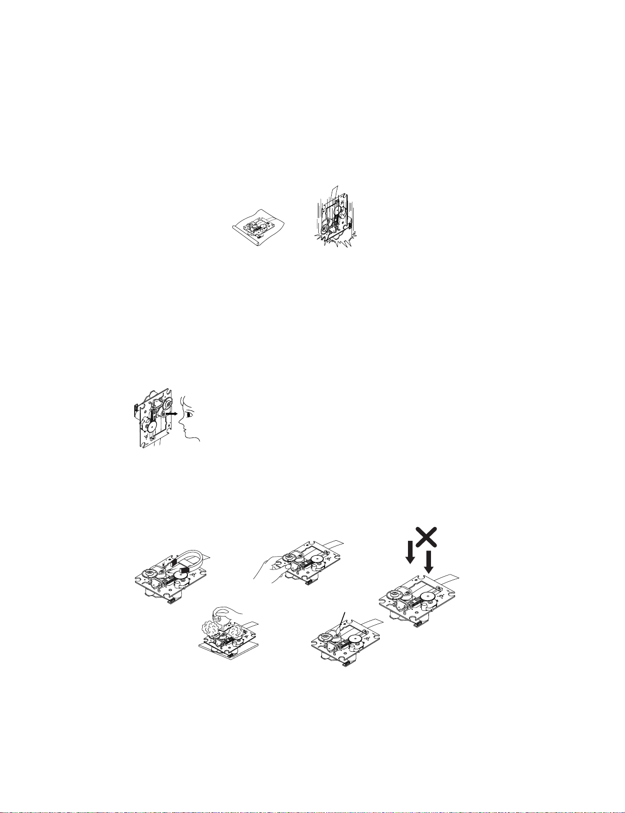
■ NOTES REGARDING HANDLING OF THE PICK-UP
1. Notes for transport and storage
1) The pick-up should always be left in its conductive bag until immediately prior to use.
2) The pick-up should never be subjected to external pressure or impact.
2. Repair notes
1) The pick-up incorporates a strong magnet, and so should never be brought close to magnetic materials.
2) The pick-up should always be handled correctly and carefully, taking care to avoid external pressure and
impact. If it is subjected to strong pressure or impact, the result may be an operational malfunction and/or
damage to the printed-circuit board.
3) Each and every pick-up is already individually adjusted to a high degree of precision, and for that reason
the adjustment point and installation screws should absolutely never be touched.
4) Laser beams may damage the eyes!
Absolutely never permit laser beams to enter the eyes!
Also NEVER switch ON the power to the laser output part (lens, etc.) of the pick-up if it is damaged.
5) Cleaning the lens surface
If there is dust on the lens surface, the dust should be cleaned away by using an air bush (such as used
for camera lens). The lens is held by a delicate spring. When cleaning the lens surface, therefore, a cotton swab should be used, taking care not to distort this.
6) Never attempt to disassemble the pick-up.
Spring by excess pressure. If the lens is extremely dirty, apply isopropyl alcohol to the cotton swab. (Do
not use any other liquid cleaners, because they will damage the lens.) Take care not to use too much of
this alcohol on the swab, and do not allow the alcohol to get inside the pick-up.
Storage in conductive bag
Drop impact
NEVER look directly at the laser beam, and don’t let
contact fingers or other exposed skin.
Magnet
How to hold the pick-up
Conductive Sheet
Cotton swab
Pressure
Pressure
Page 4
- 1-3 -
■ NOTES REGARDING COMPACT DISC PLAYER REPAIRS
1. Preparations
1) Compact disc players incorporate a great many ICs as well as the pick-up (laser diode). These components
are sensitive to, and easily affected by, static electricity. If such static electricity is high voltage, components
can be damaged, and for that reason components should be handled with care.
2) The pick-up is composed of many optical components and other high-precision components. Care must be
taken, therefore, to avoid repair or storage where the temperature of humidity is high, where strong magnetism is present, or where there is excessive dust.
2. Notes for repair
1) Before replacing a component part, first disconnect the power supply lead wire from the unit
2) All equipment, measuring instruments and tools must be grounded.
3) The workbench should be covered with a conductive sheet and grounded.
When removing the laser pick-up from its conductive bag, do not place the pick-up on the bag. (This is
because there is the possibility of damage by static electricity.)
4) To prevent AC leakage, the metal part of the soldering iron should be grounded.
5) Workers should be grounded by an armband (1M Ω)
6) Care should be taken not to permit the laser pick-up to come in contact with clothing, in order to prevent
static electricity changes in the clothing to escape from the armband.
7) The laser beam from the pick-up should NEVER be directly facing the eyes or bare skin.
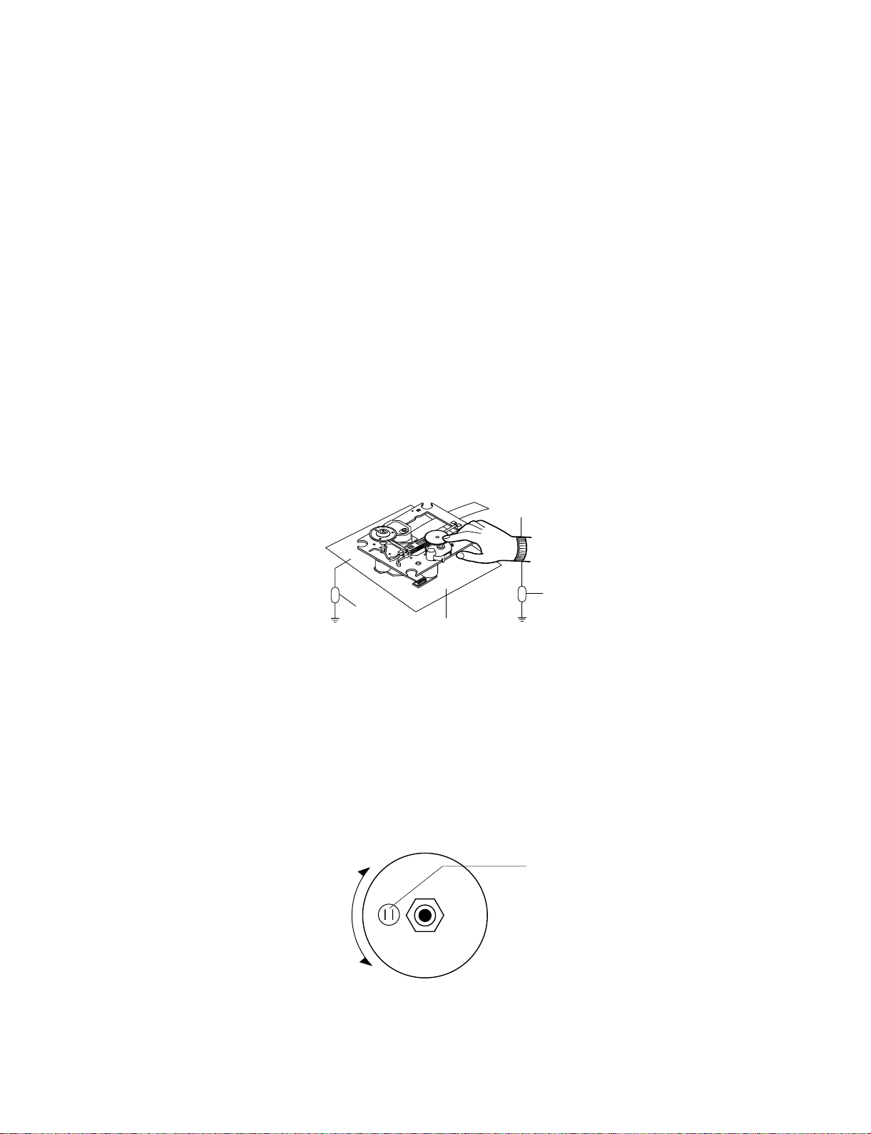
CLEARING MALFUNCTION
You can reset your unit to initial status if malfunction occur(button malfunction, display, etc.).
Using a pointed good conductor(such as driver), simply short the RESET jump wire on the inside of
the volume knob for more than 3 seconds.
If you reset your unit, you must reenter all its settings(stations, clock, timer)
NOTE: 1. To operate the RESET jump wire, pull the volume rotary knob and release it.
2. If you wish to operate the RESET jump wire, it is necessary to unplug the power cord.
Resistor
(1 Mohm)
Conductive
Sheet
Resistor
(1 Mohm)
Armband
RESET jump wire
VOLUME
VOLUME KNOB
DOWN
UP
Page 5
- 1-4 -
❏ ESD PRECAUTIONS
■ Electrostatically Sensitive Devices (ESD)
Some semiconductor (solid state) devices can be damaged easily by static electricity. Such components
commonly are called Electrostatically Sensitive Devices (ESD). Examples of typical ESD devices are integrated circuits and some field-effect transistors and semiconductor chip components. The following techniques
should be used to help reduce the incidence of component damage caused by static electricity.
1. Immediately before handling any semiconductor component or semiconductor-equipped assembly, drain off
any electrostatic charge on your body by touching a known earth ground. Alternatively, obtain and wear a
commercially available discharging wrist strap device, which should be removed for potential shock reasons
prior to applying power to the unit under test.
2. After removing an electrical assembly equipped with ESD devices, place the assembly on a conductive sur-
face such as aluminum foil, to prevent electrostatic charge buildup or exposure of the assembly.
3. Use only a grounded-tip soldering iron to solder or unsolder ESD devices.
4. Use only an anti-static solder removal device. Some solder removal devices not classified as "anti-static"
can generate electrical charges sufficient to damage ESD devices.
5. Do not use freon-propelled chemicals. These can generate electrical charges sufficient to damage ESD
devices.
6. Do not remove a replacement ESD device from its protective package until immediately before you are
ready to install it. (Most replacement ESD devices are packaged with leads electrically shorted together by
conductive foam, aluminum foil or comparable conductive materials).
7. Immediately before removing the protective material from the leads of a replacement ESD device, touch the
protective material to the chassis or circuit assembly into which the device will by installed.
CAUTION : BE SURE NO POWER IS APPLIED TO THE CHASSIS OR CIRCUIT, AND OBSERVE ALL
OTHER SAFETY PRECAUTIONS.
8. Minimize bodily motions when handing unpackaged replacement ESD devices. (Otherwise harmless motion
such as the brushing together of your clothes fabric or the lifting of your foot from a carpeted floor can generate static electricity sufficient to damage an ESD device).
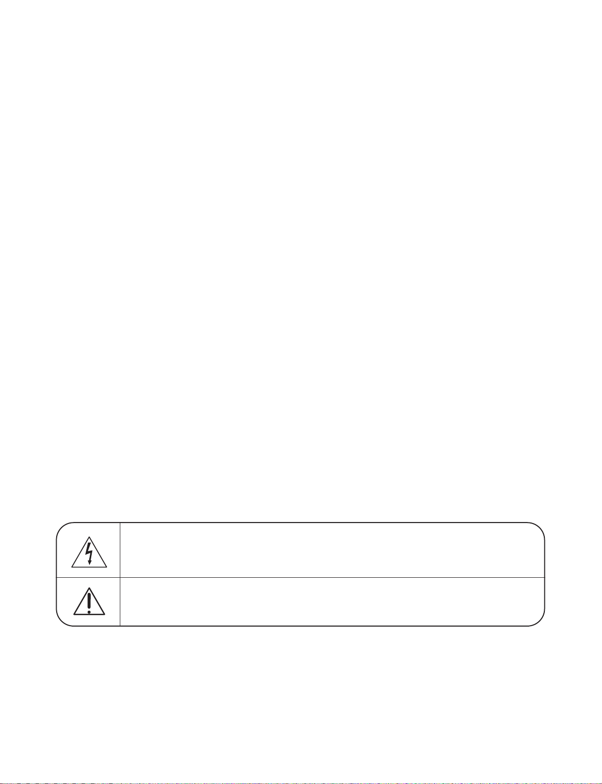
CAUTION. GRAPHIC SYMBOLS
THE LIGHTNING FLASH WITH APROWHEAD SYMBOL. WITHIN AN EQUILATERAL TRIANGLE, IS
INTENDED TO ALERT THE SERVICE PERSONNEL TO THE PRESENCE OF UNINSULATED “DANGEROUS VOLTAGE” THAT MAY BE OF SUFFICIENT MAGNITUDE TO CONSTITUTE A RISK OF
ELECTRIC SHOCK.
THE EXCLAMATION POINT WITHIN AN EQUILATERAL TRIANGLE IS INTENDED TO ALERT THE
SERVICE PERSONNEL TO THE PRESENCE OF IMPORTANT SAFETY INFORMATION IN SERVICE
LITERATURE.
Page 6

- 1-5 -
❏ SPECIFICATIONS
[GENERAL]
Power supply Refer to the back panel of the unit.
Power consumption Refer to the back panel of the unit.
Net Weight 6.2 kg
External dimensions (W x H x D) 273 x 321x 359 mm
[CD]
Frequency response 40 - 20000 Hz
Signal-to-noise ratio 75 dB
Dynamic range 75 dB
[TUNER]
FM
Tuning Range 87.5 - 108.0 MHz
Intermediate Frequency 10.7 MHz
Signal to Noise Ratio 60/55 dB
Frequency Response 50 - 10000 Hz
AM [MW]
Tuning Range 522 - 1620 kHz or 520 - 1720 kHz
Intermediate Frequency 450 kHz
Signal to Noise Ratio 30 dB
Frequency Response 140 - 1800 Hz
[AMP]MPLIFIER(LH-W96’s)
Output Power 100W +100W+150W [LM-U1560+LMS-U1560W(SUB WOOFER)]
100W+100W [LM-U1060]
50W +50W [LM-U560]
30W + 30W [LM-U360]
T.H.D 0.5%
Frequency Response 40 - 20000 Hz
Signal-to-noise ratio 75 dB
[TAPE]
Tape Speed 4.75cm/sec
Wow Flutter 0.25% (MTT -111, JIS-WTD)
F.F/REW Time 120sec (C-60)
Frequency Response 250 - 8000Hz
Signal to Noise Ratio 43dB
Channel Separation 50dB(P/B)/45dB(R/P)
Erase Ratio 55dB (MTT-5513)
[SPEAKERS]
MODEL LMS-U1560 LMS-U1560W LMS-U560 LMS-U360
LMS-U1060 (SUB WOOFER)
Type 2way 2speaker 1way 1speaker 2way 2speaker 2way 2speaker
Impedance 4Ω 3Ω 4Ω 4Ω
Frequency Response 50-20000Hz 50-15000Hz 55-20000Hz 55-20000Hz
Sound Pressure Level 85dB/W (1m) 84dB/W (1m) 86dB/W (1m) 86dB/W (1m)
Rated Input Power 100W 180W 50W 30W
Max. Input Power 200W 360W 100W 60W
Net Dimensions (W x H x D)
229X224X286mm 273x325x384mm 229X224X286mm 229X224X286mm
Net Weight 3.8kg 6kg 3.9kg 3.8kg
Page 7

- 1-6 -
Page 8
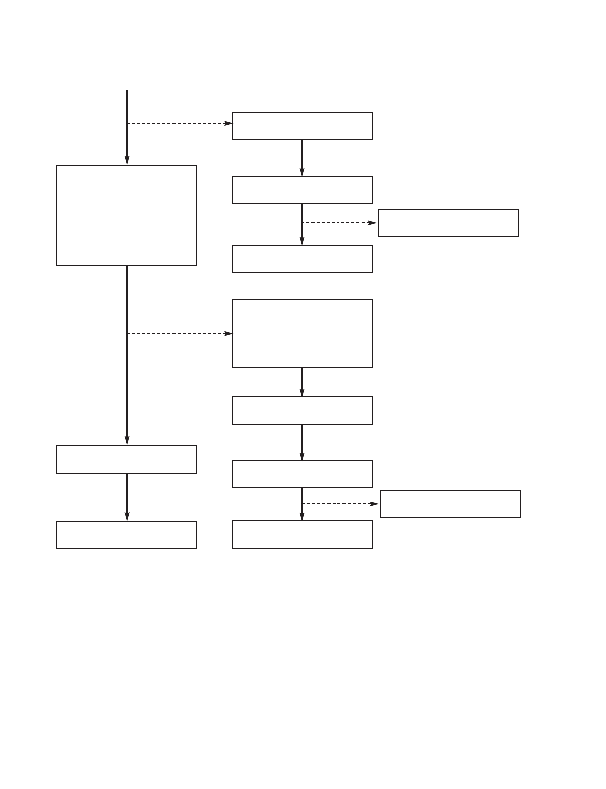
- 2-1 -
SECTION 2. ELECTRICAL
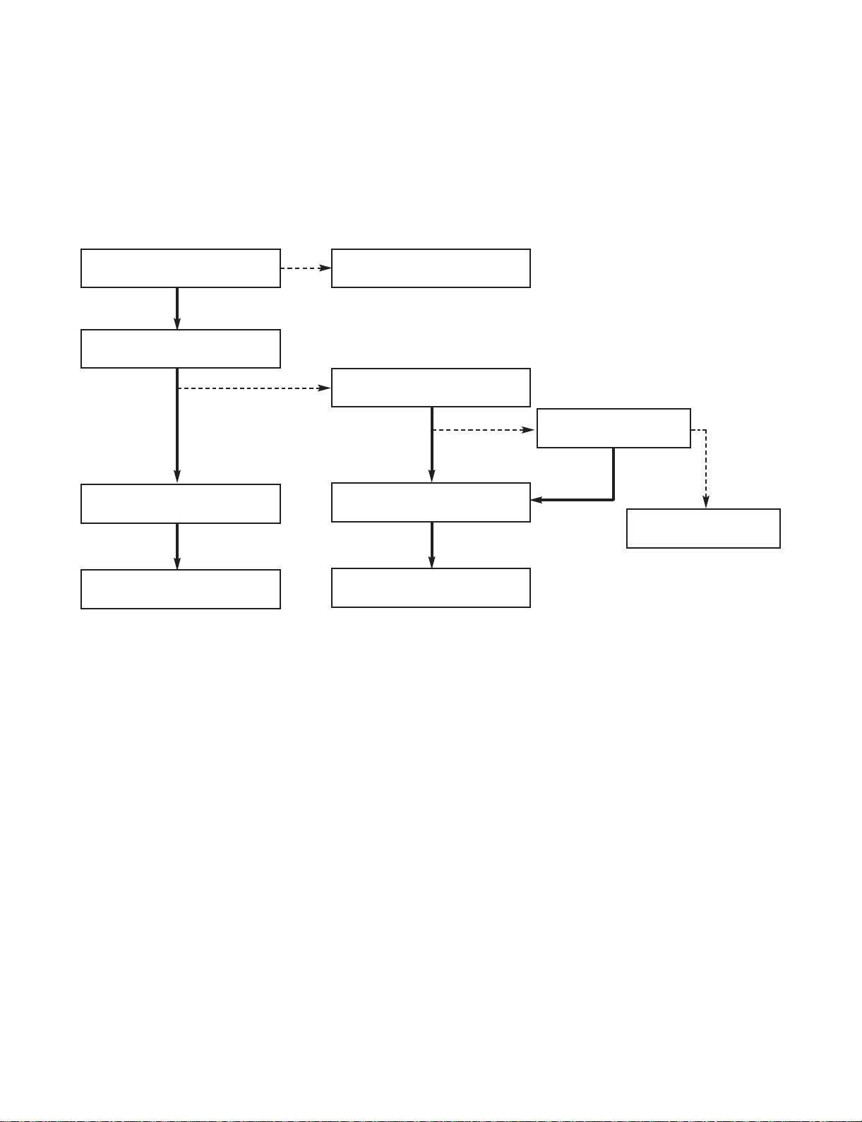
❏
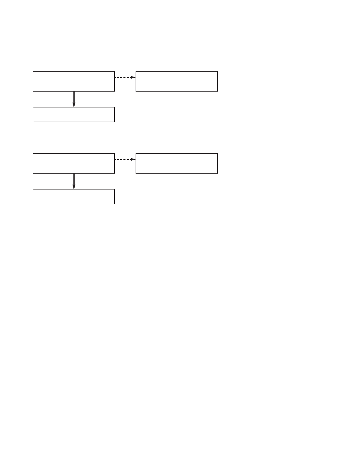
ELECTRICAL TROUBLESHOOTING GUIDE(AUDIO PART)
P7904 6PIN P-SENS check
Refer to SMPS
Troubleshooting
Check if IC101 KIA7042
input is over 5V
Check if IC101 KIA7042
input is over 4.3V
IC101 KIA7042
relevant parts check
relevant parts
replacement
normal
IC101 KIA7042?
IC100 78KO/KF2 1 PIN
Power Check
normal
YES
NO
NO
NO NO
YES
YES
YES
YES
■ MICOM PART CHECK I
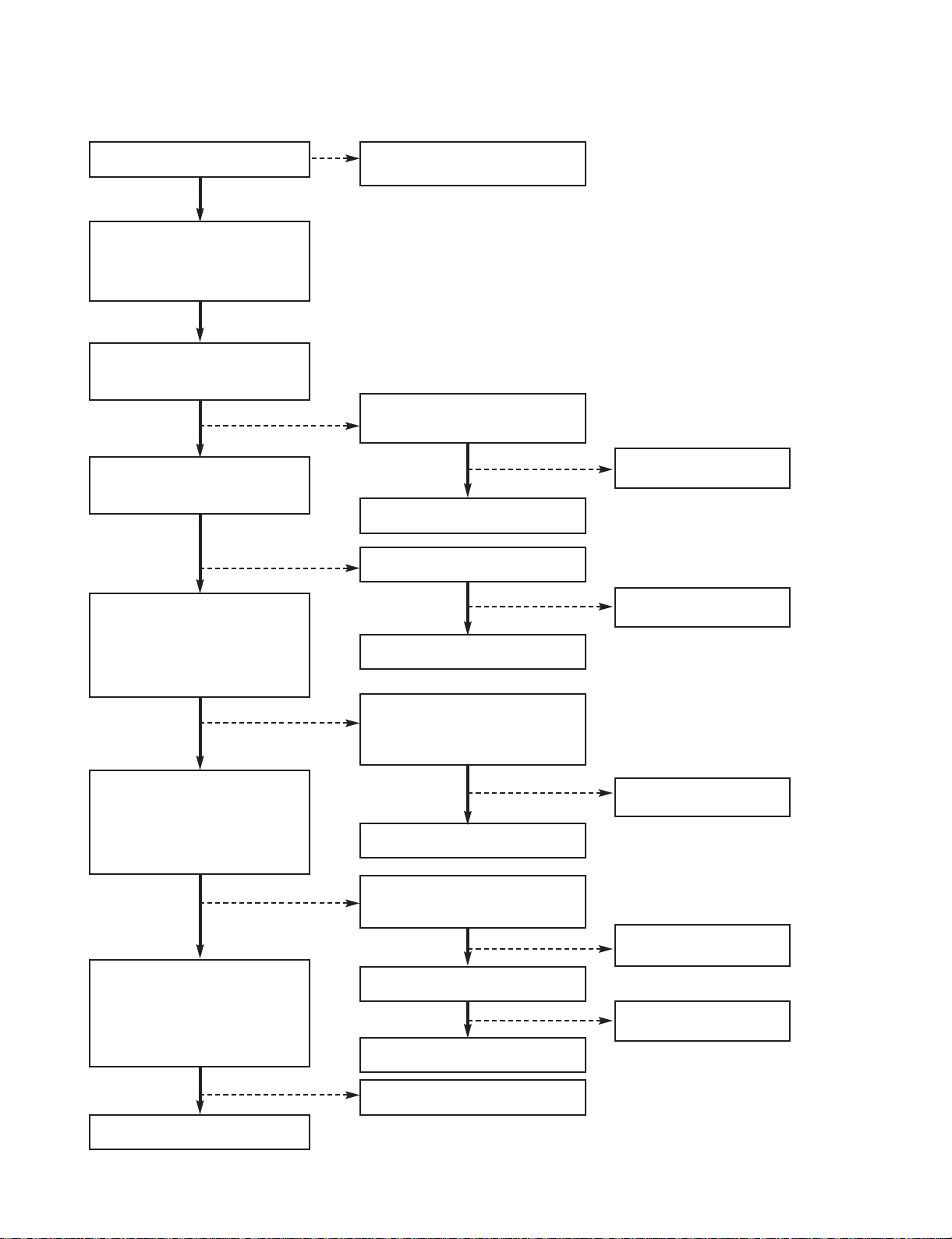
Page 9
- 2-2 -
■ MICOM PART CHECK II
Q102 BASE PIN
0.6V HIGH check
Q102 COLLECTOR
0.6V LOW check
Check if IC101
KIA7042 output
power is over 4.3V
relevant parts check
relevant parts
replacement
normal
relevant parts
replacement
relevant parts check
normal
IC 103 8PIN IC 100 19,20,59
PIN 5V check
X101:32.768KHz
X100:9.8304MHz operation
status check
normal
P7904 5PIN 5.6V check
Refer to SMPS
Troubleshooting
Output 5V operation check
D101 1SR35
relevant parts check
normal
relevant parts
replacement
D101 1SR35 both terminal
power check
Q101 EMITTER 5V check
and COLLECTO
NO
NO
NO
NO
NO
YES
YES
YES
YES
YES
YES
YES
YES
YES
YES
YES
YES
Page 10
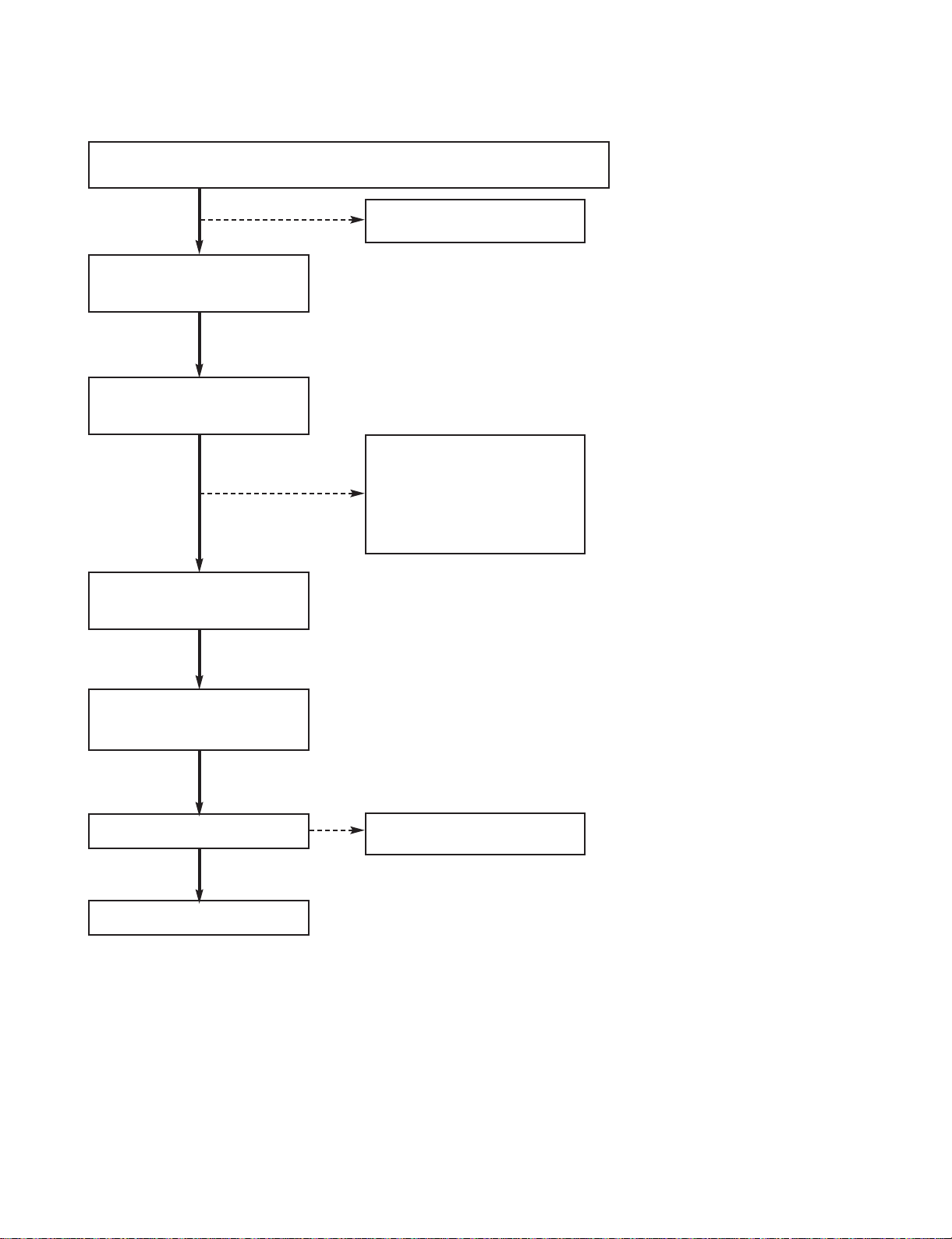
- 2-3 -
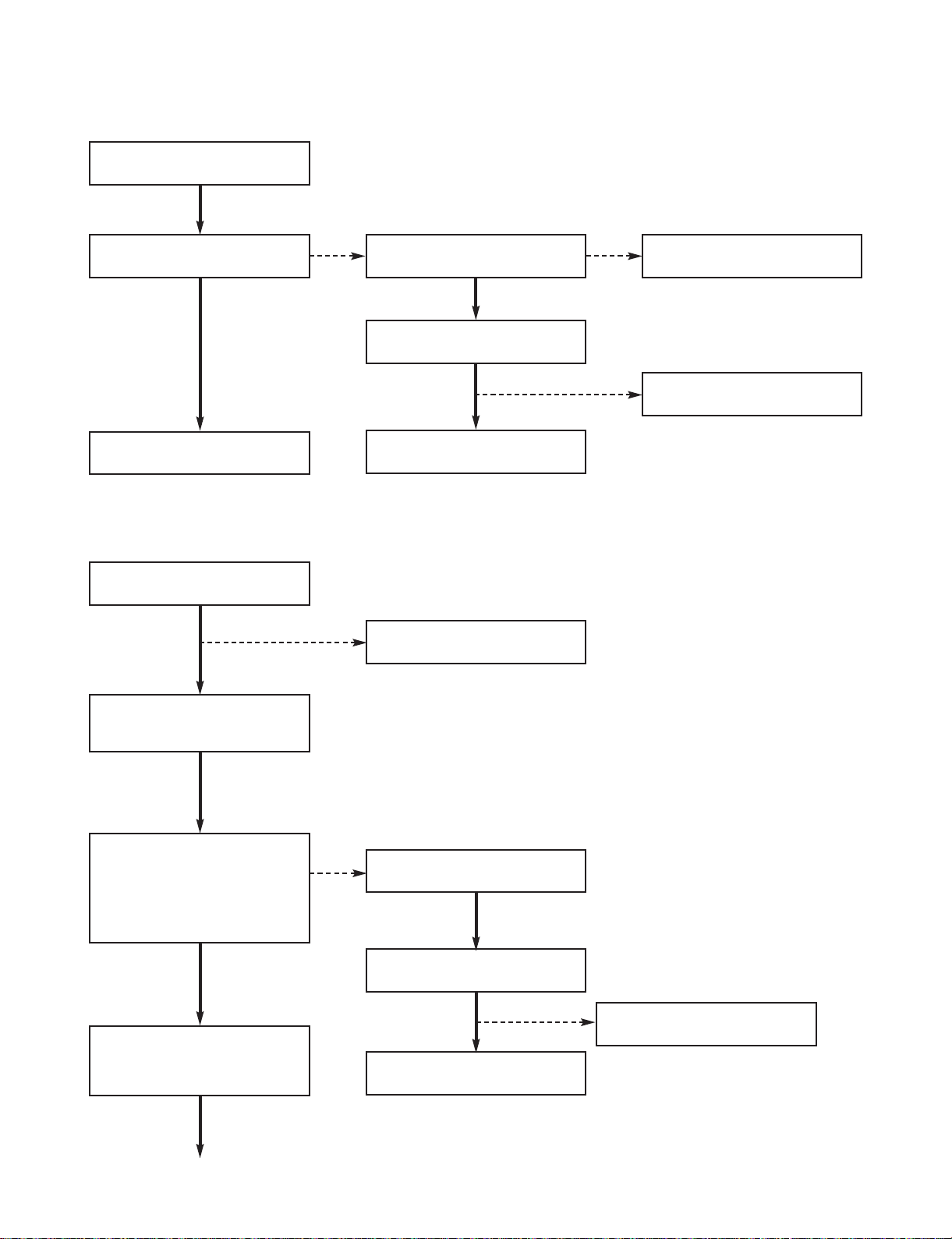
■ IC103 KS4CD21CS CHECK
IC100 78KOKF2 22,24
PIN Check
■ FLD DISPLAY CHECK
22 PIN DATA MICOM power 5V check
Refer to MICOM
Troubleshooting
relevant parts
replacement
relevant parts check
normal
Refer to SMPS
Troubleshooting
P7302 assembly check
Each PIN power check
normal
relevant parts
replacement
normal
P7904 1,2,3 power check
F1+, F2 both terminal: 5V and
above VKK: power is over 26V
P7302 connection status
check and power check
F+,F2- both termainal: 5V or
above VKK:26V or above
power check
IC301 PT6324 Power check
50 PIN VKK:-26V 9, 51
PIN +5V
YES
YES
YES
YES
YES
YES
YES
YES
YES
YES
NO
NO
NO
NO
NO
NO
Page 11
- 2-4 -
IC100 ➞ IC301 DATA
Communication check
PIN PIN
(ST8)75 PIN ➞ 3PIN(STB)
(DO) 76 PIN ➞ 2PIN(DO)
(DI) 77 PIN ➞ 4PIN(DI)
(CLK)78 PIN ➞ 1PIN(CLK)
If 5V defective D321 SR35
input and output power check
relevant parts check
76 PIN ➞ DATA input check
relevant parts check
relevant parts
replacement
normal
relevant parts
replacement
normal
FLT light on
normal
IC100
(STB)75 PIN ➞ (STB)
(DO) 77 PIN ➞ 4PIN(DO)
(CLK) 78 PIN ➞ 1PIN(CLK)
Data output check
YES
YES
YES
YES
YES
YES
YES
YES
NO
NO
NO
NO
Page 12
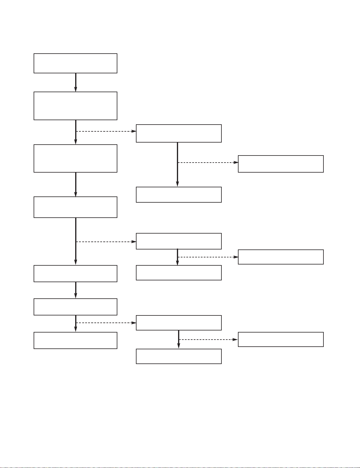
- 2-5 -
■ PWM ALTERATION PART CHECK
P7905 9PIN 3.3V check
X601 12.288MHz operation
check
IC604 PS9829
86 PIN CLK input check
IC100 78KOKF2
21 ➞ PWM_CLK
22 ➞ PWM_DATA
23 ➞ PWM_REST
output check
IC604 PS9829 DATA input
check
78 PIN ➞ DATA
79 PIN ➞ CLK
96 PIN ➞ REST
PWM MODULATOR output
check
FL:75(+)74(-)FR:71(+)70(-)
SW:68(+)67(-)
normal
IC604 PS9829 VDD PIN
Power check
(3.10.22.29.39.47.56.65.72.
87. 94)
Refer to SMPS
Troubleshooting
relevant parts check X604
12.288MHz
normal
R668(470Ω) output check
normal
LINE resistance check
DATA:R671 CLK:R670
RST:R665
normal
CD ASS`Y PS9829 communication status check(P7403)
IC604 PS9829 DATA input check
normal
IC604 PS9829 parts check
relevant parts
replacement
relevant parts
replacement
relevant parts
replacement
Refer to CD
Troubleshooting
Check each line
resistance check
YES
YES
YES
YES
YES
YES
YES
YES
YES
YES
YES
YES
NO
NO
NO
NO
NO
NO
NO
NO
NO
NO
NO
Page 13
- 2-6 -
■ POWER AMP PART CHECK
P7905 3 PIN+12 13.14.15
PIN [ LM-U1560 : 32V/LM-U1060 : 32V/LM-U560 : 22V/LM-U360 : 16V ]
Each IC700,701 34, 29, 26,
21 PIN input power check
Each IC700, 701 1, 36.17,
18, 19 PIN +12V input power
check
PWM MODULATOR input
power check Each IC
4.6.14.16 PIN
POWER IC 700.701.702.703
34.29.27.20 PIN output
check
Output LINE COIL check
normal
Refer to SMPS
Troubleshooting
Each LINE resistance output
power check
IC700:R702, 701, 726, 727,
724
IC701:R730, 729, 750 ,753,
752(Only LM-U1560)
relevant parts
replacement
YES
YES
YES
YES
YES
YES
NO
NO
NO
Page 14
- 2-7 -
■ AUX FUNCTION
Check whether JK800
contacts or not
IC200
(BU4052)4,11PI
N input waveform check
IC200
(BU4052)3,13PIN output
waveform check
IC801 (MC4580) 3, 5 PIN
input waveform check
IC801(MC4580) Pins 1, 7
output check
IC603(CS5340) Pins10, 12
input check
normal
IC200 (BU4052)16PINVDD,
8PIN VSS power check
µ-COM (IC100) 3, 6PIN
Communication check
Refer to SMPS
Troubleshooting
IC603 Pins2, 7, 8 check
relevant parts
replacement
IC801 (MC4580)4PIN
VSS,8PIN VDD power check
relevant parts
replacement
IC603 Pin4 SDout check
Relevant Part repplacement
YES
YES
YES
YES
YES
YES
YES
YES
YES
NO
NO
NO
NO
NO
NO
Page 15
- 2-8 -
■ TUNER FUNCTION CHECK
Tuner module (TUN800)
operation check
■ TAPE FUNCTION CHECK
TUNER MODUEL power
check (2PIN 9Vcheck)
IC200 (BU4052)16PIN-
VDD,8PIN VSS power check
IC801(MC4580)4PIN
VSS,8PIN VDD power check
IC200 (BU4052)16PINVDD,8PIN VSS power check
IC200(BU4052)1,
12PIN input waveform check
IC200 (BU4052)3,13PIN
output waveform check
IC601(BU4052)2,15PIN
input waveform check
IC801 (MC4580)2,6PIN input
waveform check.
TAPE PCB ASS`Y
IC801 (MC4580)2,6PIN input
check
IC200(BU4052)2,1
5PIN input waveform check
IC200 (BU4052)3,13PIN
output check IC601(BU4052)
2,15PIN input waveform
check
YES
YES
YES
IC801(MC4580) Pins 1, 7
input check
YES
IC603(CS95340) Pins10, 12
input check
YES
IC801(MC4580) Pins 1, 7
input check
IC603(CS95340) Pins10, 12
input check
YES
YES
YES
YES
YES
NO
NO YES
NO
NO
relevant parts replacement
YES
relevant parts replacement
YES
relevant parts replacement
IC200 (BU4052)16PINVDD,8PIN VSS power check
NO YES
relevant parts replacement
Page 16
- 2-9 -
■ TAPE PLAY PART CHECK
P2707:4 PIN ➞ 12V
IC201 (HA12237)16 PIN 12V
input waveform check
IC201:5.26 PIN
Signal Output check
IC20114 PIN MUTE
operation check
normal
Refer to SMPS
Troubleshooting
DECK HEAD input check
DECK HEAD input IC201
32.39 PIN check
HEAD WIRE or
Mecha replacement
relevant parts
replacement
relevant parts
replacement
relevant parts check
normal
IC202 10 PIN HIGH operation
check
relevant parts check
normal
YES
YES
YES
YES
YES
YES
YES
YES
YES
NO
NO
NO
NO
NO
NO
Page 17
- 2-10 -
■ TAPE REC PART CHECK
IC604 PS9829 #49,#52 PWM
output check
Refer to PWM modulation
part
Q601 Collector waveform check
Board to Board cantact check
IC203 8 PIN +12V check
relevant parts check
normal
Q205(D1304)
BASE HIGH check
IC202 4 PIN HIGH operation
check
Refer to SMPS
Troubleshooting
relevant parts
replacement
relevant parts
replacement
normal
P7207 #2.#4 output check
P2707 #5.#7 input check
IC203 MC4580 #1,#7 check
IC201 7.24 PIN REC input
check
IC201 10.21 PIN output
check
L203 2.3 PIN oscillation check
P2203 5.3 PIN input check
8 PIN ERASE input check
normal
YES
YES
YES
YES
YES
YES
YES
YES
YES
YES
YES
YES
NO
NO
NO
NO
NO
NO
NO
NO
Page 18
- 2-11 -
■ SMPS POWER CIRCUIT
Check the fuse F901
Check the DC V of C905.
If DC V is over 400V
Check the DC V Of
C981,C945. If DC V is 6.1V
OK
Chcek the DC VOf
C950,C951 If DC V is in
35V,-35V
Chcek the DC V Of C909,
C903,C921 If DC V is in
14~19V and it is steady.
Replace the fuse
Check BD901, LF901,902
Check IC901 ,902 Replace IC 901,902
Check short of P9702 line
Check short of P9701 line
Check short of P9701,P9702
line
*MAIN PART
YES
NO
YES
YES
YES
YES
YES
NO
NO NO
NO
NO
Page 19
- 2-12 -
Check the PIN6 OF P9702
If DC V is over 5.6V
OK
Check power circuit Trouble
shooting
*P-SENS PART (OPTIONAL PART)
Check the PIN3 OF P9702
If DC V is over -28V ±2
OK
Check power circuit
Trouble shooting
*VKK PART
YES
YES
NO
NO
Page 20
- 2-13 -
❏ INTERNAL BLOCK DIAGRAM of ICs
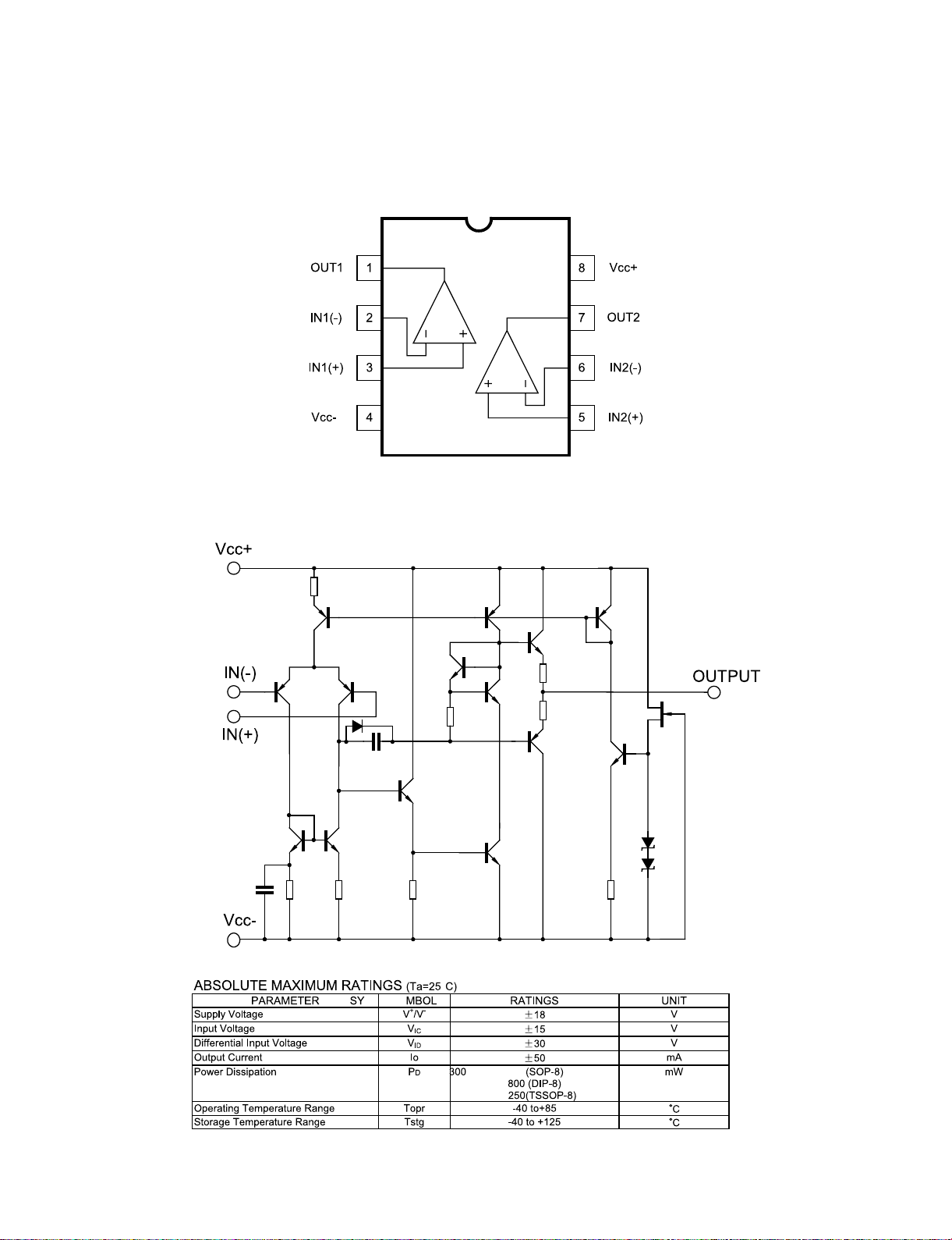
• UTC MC4580
PIN CONFIGURATION
TEST CIRCUIT
Page 21

- 2-14 -
• FAN8082D
Internal Block Diagram
Page 22

- 2-15 -
• BU2090
Block diagram
Page 23

- 2-16 -
• BA3308 / BA3308F
BLOCK DIAGRAM
BA3308
BA3308F
Page 24

- 2-17 -
• HT1200-4
SYSTEM BLOCK DIAGRAM
Page 25

- 2-18 -
• HT1200-4
FUNCTIONAL BLOCK DIAGRAM
Page 26

- 2-19 -
• CS5340
BLOCK DIAGRAM
• BU4052
BLOCK DIAGRAM
Page 27

- 2-20 -
• HA12237F
BLOCK DIAGRAM
Page 28

- 2-21 -
• PT6324
BLOCK DIAGRAM
Page 29

- 2-22 -
❏
ELECTRICAL TROUBLESHOOTIHG GUIDE & WAVEFORM(CD PART)
■ POWER CHECK GUIDE
Y
Y
N
Y
Y
Y
N
N
N
N
Y
POWER ON
POWER ON
DOES CD
APPEAR AT FLD?
DOES DISK1
APPEAR AT FLD?
CHECK THE
VOLTAGE OF EACH PIN
ON P5701.
CHECK CD MD MODULE.
CHECK CONNECTOR
P7501.
RECONNECT IT.
OK.
DOES AUX,FM 87.5
APPEAR AT FLD?
DOES IT
APPEAR CD
ERROR AT FLD?
PUSH KARAOKE
CD BUTTON
CHECK
CONNECTOR (P4703,P4004,
P5701)
OK
DOES NO DISC OR
TIME ARE APPEARED
AT FLD?
Page 30

- 2-23 -
TURN ON CD
OPEN CLOSE CHECK
CONNECTOR CHECK
( PN803, PN804 )
CHECK Voltage CN806
PIN1:12, PIN2:6.3V
“ READING ”
DISPLAY CHECK
READING OK CHECK
IF PLAY, AUDIO
OUTPUT CHECK
OK
CHECH Vtg PN805 PIN22 :
CLOSE,PIN23:OPEN
CONNECTOR CHECK (PN802,
PN803, PN804, CN806,PN814 )
CHECK MICOM INTERFACE CIRCUIT( PN805 )
(CE,BTL-MUTE,CD-IN,CDOUT,CLK,WRQ,FSEQ)
CONNECTOR
CHECK(PN801,PN802)
CHECK PICKUP MOVEMENT
CHECK AM5810FP (IC802)
CHECK LC78692 (IC801)
CHECK PN805 AUDIO DATA
PIN10 : DA_LRCK (IC801 PIN60 LRSY)
PIN11 : DA_BCK (IC801 PIN59 DATACLK)
PIN12 : DA_DATA0 (IC801 PIN58 DATA)
■ CD PART
Page 31

- 2-24 -
CONNECTOR LOCKING CHECK
( PN803, PN804, PN814 )
CHECK POWER SUPPLY CIRCUIT ( PN805, CN806)
CN806 PIN1:12V, PIN2:6.3V, PN805 PIN8:+5V_AD
DEFECTIVE MAIN POEWR SUPPLY
CHECK VOLTAGE CHANGE OF OPEN CLOSE IC803 INPUT VOLTAGE
PIN6:12V, PIN7:6.3V (PN805 PIN2:BTL_MUTE, 23:OPEN, 22:CLOSE)
CHECK VOLTAGE CHANGE LO+, LO- OF
IC803 (PN805 PIN23:OPEN, PIN22:CLOSE)
DEFECTIVE MECHANISM
DEFECTIVE MICOM
DEFECTIVE IC803
■ OPEN CLOSE NG
Page 32

- 2-25 -
CONNECTOR LOCKING CHECK
(PN802, PN803,PN804,PN805,CN806 )
CHECK POWER SUPPLY PORT( PN805,
CN806) CN806 PIN1: 12V, PIN2: 6.3V,
PIN4: 5V PN805 PIN8 = 5V_AD
DEFECTIVE CONNECTOR OR
MAIN POWER SUPPLAY
CHECK VOLTAGE THE PIN 2 OF IC804
IC804 PIN2 : 3.3V
CHECK RESET SIGNAL OF PN805
PN805 PIN19: 5V
CHECK MICOM INTERFACE CIRCUIT( PN805 )
PN805 PIN 1,3,4,15,19,26 SIGNAL CHECK
(1: CE, 3: DI, 4: CLK, 15: D0, 19: RST, 18:
FSEQ, 26: WRQ)
PIN3 DI : FROM DSP TO MICOM
PIN15 DO: FROM MICOM TO DSP
CHECK THE WAVE FORM #1
DEFECTIVE IC801
DEFECTIVE IC804
DEFECTIVE MICOM OR CONNECTOR
DEFECTIVE MICOM OR CONNECTOR
■ “ READING ” DISPLAY CHECK (= ONLY “CD” DISPLAY)
Page 33

- 2-26 -
CONNECTOR LOCKING
CHECK(PN801,PN802)
DOES SLED MOVE ?
CHECK PN802
PIN 3,4( SL+,SL-)
DOES LENSE MOVE ?
(= UP & DOWN)
DOES LASER LIGHT ?
DOES SPINDLE ROTATE ?
IS READING OK ?
DEFECTIVE PICKUP OR
IC802 OR IC801
CHECK PN801
PIN 13,16 ( FA+,FA-)
A
B
C
D
E
DEFECTIVE PICKUP OR
IC802 OR IC801
CHECK PN801 PIN 10( LD )
CHECK PN802
PIN 5,6( SP+,SP-)
CHECK PN801
PIN 14,15 (TA+,TA-)
DEFECTIVE PICKUP OR
IC801
DEFECTIVE PICKUP OR
IC802 OR IC801
DEFECTIVE PICKUP OR
IC802 OR IC801
■ READING OK CHECK (= “NO DISC” DISPLAY)
Page 34

- 2-27 -
DOES SL+ WAVEFORM
APPEAR AT ( IC802 PIN13
AND PN 802 PIN3) WAVE-
FORM #2 SLED MOTOR
WAVE
DEFECTIVE IC802
CHECK PN802
CONNECTOR LINE
DEFECTIVE PICKUP
SLED MOTOR
DOES SLIN WAVEFORM
APPEAR AT ( IC802 PIN5)
WAVEFORM #2 SLED
DRIVE WAVE
DEFECTIVE IC801
DEFECTIVE PN802
CONNECTOR
■ READING OK CHECK #A (= “NO DISC” DISPLAY)
A
Page 35

- 2-28 -
DOES FA+ WAVEFORM
APPEAR AT ( IC802 PIN16
AND PN801 PIN13) WAVE-
FORM #3 FOCUS COIL
DRIVE WAVE
DEFECTIVE IC802
CHECK PN801
CONNECTOR LINE
DEFECTIVE PICKUP
FOCUS ACTUATOR
DOES FAINWAVEFORM
APPEAR AT ( IC802 PIN 25)
WAVEFORM #3 FOCUS
DRIVE WAVE
DEFECTIVE IC801
DEFECTIVE PN801
CONNECTOR
■ READING OK CHECK #B (= “NO DISC” DISPLAY)
B
Page 36

- 2-29 -
IS ?V APPLIED TO PIN10 OF
PN801
LASER SUPPLY VOLTAGE
CHECK
IS 2.3 V PIN18(LDO) OF
IC801 LASER CONTROL
VOLTAGE CHECK
CHECK PN801
CONNECTOR LINE
DEFECTIVE PN801
CONNECTOR
DEFECTIVE PICKUP
LASER PART
IS 3.3 V APPLIED TO PIN30,
36, 39, 41, 61, 68, 75 OF
IC801
RF IC SUPPLY VOLTAGE
CHECK
DEFECTIVE IC804
DEFECTIVE IC801
DEFECTIVE Q801 OR
D801
■ READING OK CHECK #C (= “NO DISC” DISPLAY)
C
Page 37

- 2-30 -
DOES SP+ WAVEFORM
APPEAR AT ( IC802 PIN11
AND PN802 PIN 5) WAVEFORM #4 SPINDLE MOTOR
DRIVE WAVE
DEFECTIVE IC802
CHECK PN802
CONNECTOR LINE
DEFECTIVE PN802
CONNECTOR
DEFECTIVE PICKUP
SPINDLE MOTOR
DOES SPIN WAVEFORM
APPEAR AT (IC802 PIN6)
WAVEFORM #4
SPINDLE DRIVE WAVE
DEFECTIVE IC801
■ READING OK CHECK #D (= “NO DISC” DISPLAY)
D
Page 38

- 2-31 -
DOES TA+ WAVEFORM
APPEAR AT ( IC802 PIN17
AND PN801 PIN14)
WAVEFORM #5 TRACKING
COIL DRIVE WAVE
DEFECTIVE IC802
CHECK PN802
CONNECTOR LINE
DEFECTIVE PN802
CONNECTOR
DOES ARF SIGNAL APPEAR?
(IC801 PIN 2 ) WAVEFORM #6
DOES TAINWAVEFORM
APPEAR AT ( IC802 PIN 22)
WAVEFORM #5 TRACKING
DRIVE WAVE
DEFECTIVE IC801
DEFECTIVE PICKUP
OR IC801
DOES FE, TE SIGNAL
APPEAR? (IC801
PIN10:RFMON , PIN16:TE)
WAVEFORM #6
* REMON IS FE
DEFECTIVE PICKUP
OR IC801
■ READING OK CHECK #E (= “NO DISC” DISPLAY)
E
Page 39

- 2-32 -
■ USB PART
TURN ON USB
“ CHECKING ” OR “USB” DISPLAY CHECK
CONNECTOR CHECK
( PN805, CN806, PN810 )
READING OK CHECK
IF PLAY, AUDIO OUTPUT CHECK
OK
CHECK POWER SUPPLY CIRCUIT( CN806 )
CHECK PN810 1 PIN : 5V
CHECK PN810 PIN 2(D-), 3(D+)
CHECK OTI6888 (IC805)
CHECK SIGNAL STCK,STREQ,STDATA
STCK : IC805 PIN52 , IC801 PIN 55
STREQ : IC805 PIN53 , IC801 PIN 54
STDATA: IC805 PIN54 , IC801 PIN 56
CONNECTOR CHECK (CN806)
CHECK MICOM INTERFACE CIRCUIT( PN805 )
PIN13: RX (IC805 PIN49 :TXD)
PIN14: TX (IC805 PIN33 : RXD)
Page 40

- 2-33 -
■ WAVEFORMS OF MAKOR CHECK POINT
#1. MICOM INTERFACE WAVEFORM
(PN805 PIN 26, 19, 3, 15) DURING POWER ON
PIN 26 : WRQ
PIN 19 : RESET
PIN 3 : DI (IC801 PIN46 DATA OUT)
PIN 15 : DO (IC801 PIN45 DATA IN)
#2. MICOM INTERFACE WAVEFORM
(PN805 PIN 26, 19, 3, 15) DURING NORMAL PLAY
PIN 26 : WRQ
PIN 19 : RESET
PIN 3 : DI (IC801 PIN46 DATA OUT)
PIN 15 : DO (IC801 PIN45 DATA IN)
#1. MICOM INTERFACE WAVEFORM
(PN805 PIN 4, 1, 18) DURING POWER ON
PIN 1 : CE
PIN 4 : CL
PIN 18 : FSEQ
#1. MICOM INTERFACE WAVEFORM
(PN805 PIN 4, 1, 18) DURING NORMAL PLAY
PIN 4 : CL
PIN 1 : CE
PIN 18 : FSEQ
Page 41

- 2-34 -
■ WAVEFORMS OF MAKOR CHECK POINT
#2. SLED DRIVE AND MOTOR WAVEFORM
(IC802 PIN 5, 13) WHEN FOCUS SEARCH
PIN 5 : SLIN
PIN 13 : SL+
#2. MICOM INTERFACE WAVEFORM
(PN805 PIN 26, 19, 3, 15) DURING NORMAL PLAY
PIN 26 : WRQ
#3. FOCUS DRIVE AND MOTOR WAVEFORM
(IC802 PIN 25, IC802 PIN 16)
• WHEN FOCUS SEARCH FAILED OR THERE IS
NO DISC ON TRAY
#3. FOCUS DRIVE AND MOTOR WAVEFORM
(IC802 PIN 25, IC802 PIN 16)
• THERE IS DISC ON TRAY AND FOCUS SEARCH
SUCCESS
PIN 5 : SLIN
PIN 13 : SL+
PIN 25 : FAO
PIN 25 : FAO
PIN 16 : FA+
PIN 16 : FA+
Page 42

- 2-35 -
■ WAVEFORMS OF MAKOR CHECK POINT
#4. SPINDLE DRIVE AND MOTOR WAVEFORM
(IC802 PIN 6, 11) WHEN TOC READING
PIN 11 : SP+
PIN 6 : SPIN
#5. TRACK DRIVE AND MOTOR WAVEFORM
(IC802 PIN 22 , IC802 PIN 17) DURING NORMAL PLAY
PIN 22 : TAO
PIN 17 : TA+
#6. RF, FOCUS AND TRACKING ERROR WAVEFORM
(IC801 PIN 2, 10, 16) DURING NORMAL PLAY
PIN 2 : RFOUT
PIN 10 : RFMON(FE)
PIN 16 : TE
Page 43

Page 44

❏ WIRING DIAGRAM
2-36 2-37
3 CHANGER MECHANISM
FRONT
A A B
EAD30732401
B
EAD30731701
C
561-7073
8PIN
MAIN
A
561-7150
C
6630XE00130
B
D
561-711H
E
6630XF00429
F G
561-843G
E
D
15P
C
3PIN
BA
CD
A
561-711C
C
561-711E
BED
6630XE00130
561-715D
G
F
561-711F
F
6630XE00816
561-
715H
8PIN
DECK
561-844G
C
561-715C
D
6630XF00415
E
561-715H
563-935H
GF
8PIN8PIN
29PIN
E
6850R-H322A
SMPS
A
6631R-F039K
B
6631R-E108H
6850R-H020A
DECK MECHANISM
29PIN
C
C B
5PIN
6PIN
F
E
4PIN
30PIN
5PIN
CD BORD
D
G
16PIN
2PIN
8PIN
D
8PIN
C
30PIN
A
A
A
B
8PIN
B
4PIN
4PIN
A
FRONT BORD
8PIN
B
8PIN
6850R-G420B
EAD30732801
Page 45

2-38 2-39
❏ BLOCK DIAGRAM
LM-U1560 : 2.1CH (100W X 2Ch + 150W)
LM-U1060 : 2CH (100W X 2Ch )
LM-U560 : 2CH (50W X 2Ch)
LM-U360 : 2CH (30W X 2Ch)
DECK
REC MUTE
P/B MUTE
A/B RETM
REC SW
REC MUTE
HA1227
TAPE IC
TUNER
MO
TAPE L/R
AUX INPUT
MIC INPUT
SOL" A"
SOL" B"
MOTER
HIGH/N
DULE
ORM
EXPENDER
OP AMP
RDS
DATA.CLK
PLL DAT.CLK
TUNER L/R
AUX L /R
EXP CLK
DATA
VFD DRIVE IC
PT632
VFD DATA.CLK
9.8304 MHz
NEC
AUDIO
MICOM
BU4052 DATA
4052
(Switch IC)
4
9829_DA
9829_RESET
9829_CLK
LEVEL METER
REC L/R
CE,DI,DO,CLK,WRQ,FSEQ
CS5340 REST
OP AMP
T
CS5340
CLK.DATA
AMP BOARDMAIN BOARD
CS5340
FLD (DISPLAY)
RESE
12.288 MHz
PS9829B
PWM
MODULATOR
LRCK,BCK,SDA TA0
12.28MHz
SD
FL+/-, FR+/-
RL+/-, RR+/-
CENTER+/-
WOOFER+/-
H/P_SW
PWM OU
T
T
(New Vers
HT1000
Power Amp
CD
SANYO
LC78692W
ion)
OP AMP
HEAD PH
D+,D-
FL
FR
S/W
LM-U1560
SUB WOOFER
ONES
USB HOST
Page 46

2-40 2-41
❏ SCHEMATIC DIAGRAMS
• MAIN SCHEMATIC DIAGRAM
A
1
2
3
4
5
6
7
8
9
10
11
12
B C D E F G H I J K L M N O P Q R ST
Page 47

2-42 2-43
• AMP SCHEMATIC DIAGRAM
A
1
2
3
4
5
6
7
8
9
10
11
12
B C D E F G H I J K L M N O P Q R ST
Page 48

2-44 2-45
• FRONT SCHEMATIC DIAGRAM
A
1
2
3
4
5
6
7
8
9
10
11
12
B C D E F G H I J K L M N O P Q R ST
Page 49

2-46 2-47
• DECK SCHEMATIC DIAGRAM
A
1
2
3
4
5
6
7
8
9
10
11
12
B C D E F G H I J K L M N O P Q R ST
Page 50

2-48 2-49
• CD SCHEMATIC DIAGRAM
A
1
2
3
4
5
6
7
8
9
10
11
12
B C D E F G H I J K L M N O P Q R ST
Page 51

2-50 2-51
• USB SCHEMATIC DIAGRAM
A
1
2
3
4
5
6
7
8
9
10
11
12
B C D E F G H I J K L M N O P Q R ST
Page 52

2-52 2-53
A
1
2
3
4
5
6
7
8
9
10
11
12
B C D E F G H I J K L M N O P Q R ST
NOTES) Symbol denotes AC ground.
NOTES) Symbol denotes DC chassis ground.
NOTE) Warning
NOTE) Parts that are shaded are critical
NOTE) With respect to risk of fire or
NOTE) electricial shock.
• SMPS SCHEMATIC DIAGRAM
IMPORTANT SAFETY NOTICE
WHEN SERVICING THIS CHASSIS, UNDER NO CIRCUMSTANCES SHOULD THE ORIGINAL DESIGN BE
MODIFIED OR ALTERED WITHOUT PERMISSION
FROM THE LG ELECTRONICS CORPORATION. ALL
COMPONENTS SHOULD BE REPLACED ONLY WITH
TYPES IDENTICAL TO THOSE IN THE ORIGINALCIR-
CUIT. SPECIALCOMPONENTS ARE SHADED ON THE
SCHEMATIC FOR EASY IDENTIFICATION.
THIS CIRCUIT DIAGRAM MAY OCCASIONALLY DIFFER FROM THE ACTUAL CIRCUIT USED. THIS WAY,
IMPLEMENTATION OF THE LATEST SAFETY AND
PERFORMANCE IMPROVEMENT CHANGES INTO
THE SET IS NOT DELAYED UNTILTHE NEW SERVICE
LITERATURE IS PRINTED.
NOTE :
1. Shaded( ) parts are critical for safety. Replace only
with specified part number.
2. Voltages are DC-measured with a digital voltmeter
during Play mode.
Page 53

2-54 2-55
❏ PRINTED CIRCUIT DIAGRAMS
• MAIN P.C. BOARD (TOP VIEW)
Page 54

2-56 2-57
• MAIN P.C. BOARD (BOTTOM VIEW)
Page 55

2-58 2-59
• FRONT P.C. BOARD
Page 56

2-60 2-61
• SMPS P.C. BOARD • DECK P.C. BOARD
(BOTTOM VIEW)
(TOP VIEW)
Page 57

2-62 2-63
• CD P.C. BOARD (TOP VIEW)
Page 58

2-64 2-65
• CD P.C. BOARD (BOTTOM VIEW)
Page 59

Page 60

3-1 3-2
SECTION 3. EXPLODED VIEWS
❏ CABINET AND MAIN FRAME SECTION
NOTES) THE EXCLAMATION POINT WITHIN AN
EQUILATERAL TRIANGLE IS INTENDED
TO ALERT THE SERVICE PERSONNEL
TO THE PRESENCE OF IMPORTANT
SAFETY INFORMATION IN SERVICE
LITERATURE.
A26
*OPTIONAL PART
258
256
255
254
252
288
253
259
A43
A44
A51
257
255
451
CABLE2
451
A50
A00
CABLE3
264
450
260
A49
A46
TUN800
A41
287
266
451
263
471
262
250
251
CABLE1
CN201
A40
A47
289
267
290
454
291
*OPTIONAL PART
300
Page 61

3-3 3-4
❏ TAPE DECK MECHANISM (A/R & A/S : LEFT A/S DECK)
023
015
022
019
037
021
020
018
017
006
A01
008
007
001
002
003
009
009
011
013
A02
025
A00
Page 62

3-5 3-6
❏ TAPE DECK MECHANISM (A/R & A/S : RIGHT A/R DECK)
016
018
007
008
015
019
021
020
017
A03
009
003
011
013
009
022
025
023
A00
Page 63

3-7 3-8
❏ DECK MECHANISM EXPLODED VIEWS
416
151
156
418
169
173
170
419
163
422
165
159
164
417
417
416
166
167
177
175
172
162
153
168
155
184
A26
Page 64

- 3-9 -
❏ SPEAKER (MODEL:LMS-U1060)
850
A80
853
862
RIGHT
859
LEFT
858
857
856
LEFT
860
RIGHT
861 RIGHT
851
LEFT
875
876
855
854
852
Page 65

- 3-10 -
 Loading...