

Page 1
SPECIFICATIONS
1. LCD CHARACTERISTICS
Type : Color TFT LCD
Size : 15.0 inch (38.1cm)
Pixel Pitch : 0.297mm x 0.297mm
Electrical Interface : LVDS Interface
Color Depth : 8-bits/ 16,194,277colors
Active Video Area : 304.1mm x 228.1mm
Surface Treatment : Anti-Glare, Hard Coating (3H)
Backlight Unit : Bottom edge side 2CCFL
(Cold Cathode Fluorescent Lamp)
2. OPTICAL CHARACTERISTICS
2-1. Viewing Angle by Contrast Ratio ≥ 10
Left : 60° typ., 50° min.
Right : 60° typ., 50° min.
Top : 55° typ., 40° min.
Bottom : 45° typ., 40° min.
2-2. Luminance : 160(min), 200(typ)
2-3. Contrast Ratio : 150(min), 250(typ)
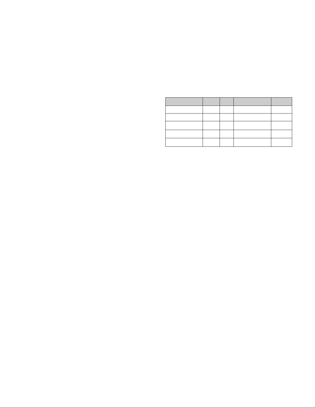
3. SIGNAL (Refer to the Timing Chart)
3-1. Sync Signal
1) Type : Separate Sync. (Horizontal & Vertical)
2) Input Voltage Level : Low=0~0.8V, High=2.1~5.5V
3) Sync Polarity : Positive or Negative
3-2. Video Input Signal
1) Type : R, G, B Analog
2) Voltage Level : 0~0.714 V
a) Color 0, 0 : 0 Vp-p
b) Color 7, 0 : 0.467 Vp-p
c) Color 15, 0 : 0.714 Vp-p
3) Input Impedance : 75 Ω
3-3. Operating Frequency
Horizontal : 31 ~ 61kHz
Vertical : 56 ~ 75Hz
4. POWER SUPPLY
4-1. Power Adaptor
Input : AC 100~240V, 50/60Hz 1.2A
Output : DC 12V 3.0A
4-2. Power Consumption
5. ENVIRONMENT
5-1. Operating Temperature: 10°C~35°C (50°F~95°F)
(Ambient)
5-2. Relative Humidity : 5%~95%
(Non-condensing)
5-3. MTBF : 40,000(Min)
6. DIMENSIONS (with TILT/SWIVEL)
Width : 389.2mm (15.32'')
Depth : 161.8mm (6.37'')
Height : 382.4mm (15.05'')
7. WEIGHT (with TILT/SWIVEL)
Net. Weight : 4.8kg (10.58 lbs)
Gross Weight : 6.8kg (14.99 lbs)
8. Audio Spec
8-1. Audio AMP
Input : 0.700Vrms
Output : 1Wrms+1Wrms
S/N : more then 40dB
8-2. Speaker
Impedance : 4
Ω
input : Max: 1.5W, Normal: 1W
MODE
POWER ON (NORMAL)
STAND-BY
SUSPEND
OFF
POWER OFF
H/V SYNC
ON/ON
OFF/ON
ON/OFF
OFF/OFF
-
POWER CONSUMPTION
less than 36 W
less than 3 W
less than 3 W
less than 3 W
less than 3 W
LED COLOR
GREEN
YELLOW
YELLOW
YELLOW
OFF
VIDEO
ACTIVE
OFF
OFF
OFF
-
Page 2
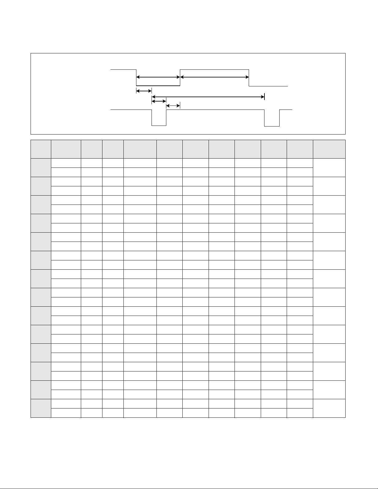
TIMING CHART
- 4 -
VIDEO
SYNC
B
D
C
F
E
A
H / V
H (Pixels)
V (Lines)
H (Pixels)
V (Lines)
H (Pixels)
V (Lines)
H (Pixels)
V (Lines)
H (Pixels)
V (Lines)
H (Pixels)
V (Lines)
H (Pixels)
V (Lines)
H (Pixels)
V (Lines)
H (Pixels)
V (Lines)
H (Pixels)
V (Lines)
H (Pixels)
V (Lines)
H (Pixels)
V (Lines)
H (Pixels)
V (Lines)
H (Pixels)
V (Lines)
Sync
Polarity
+
–
–
+
–
–
–
–
–
–
–
–
+
+
+
+
+
+
+
+
–
–
–
–
–
–
+
+
Dot
Clock
25.175
28.322
25.175
30.24
31.5
31.5
36.0
40.0
50.0
49.5
57.2832
65
75
78.75
Frequency
31.468 KHz
70.0 Hz
31.468 KHz
70.0 Hz
31.469 KHz
60.0 Hz
35.00 KHz
66.67 Hz
37.861 KHz
72.8 Hz
37.50 KHz
75.0 Hz
35.156 KHz
56.25 Hz
37.879 KHz
60.3 Hz
48.077 KHz
72.188 Hz
46.875 KHz
75.0 Hz
49.725 KHz
74.55 Hz
48.363 KHz
60.0 Hz
56.476 KHz
70.0 Hz
60.023 KHz
75.0 Hz
Resolution
640 x 350
720 x 400
(TEXT)
640 x 480
640 x 480
640 x 480
640 x 480
800 x 600
800 x 600
800 x 600
800 x 600
832 x 624
(MAC)
1024 x 768
1024 x 768
1024 x 768
Total
Period
( E )
800
449
900
449
800
525
864
525
832
520
840
500
1024
625
1056
628
1040
666
1056
625
1152
667
1344
806
1328
806
1312
800
Video
Active
Time ( A )
640
350
720
400
640
480
640
480
640
480
640
480
800
600
800
600
800
600
800
600
832
624
1024
768
1024
768
1204
768
Blanking
Time
( B )
160
99
180
49
160
45
224
45
192
40
200
20
224
25
256
28
240
66
256
25
320
43
320
38
304
38
288
32
Sync
Duration
( D )
96
2
108
2
96
2
64
3
40
3
64
3
72
2
128
4
120
6
80
3
64
3
136
6
136
6
96
3
Back
Porch
( F )
48
60
55
34
48
33
96
39
128
28
120
16
128
22
88
23
64
23
160
21
224
39
160
29
144
29
176
28
Front
Porch
( C )
16
37
17
13
16
10
64
3
24
9
16
1
24
1
40
1
56
37
16
1
32
1
24
3
24
3
16
1
MODE
1
2
3
4
5
6
7
8
9
10
11
12
13
14
Page 3
1
523
8
7
14
9
16
17
22
21
6
11
10
2
15
18
3
13
12
20
4
MIC.
IN
AUDIO
IN
MIC.
OUT
19
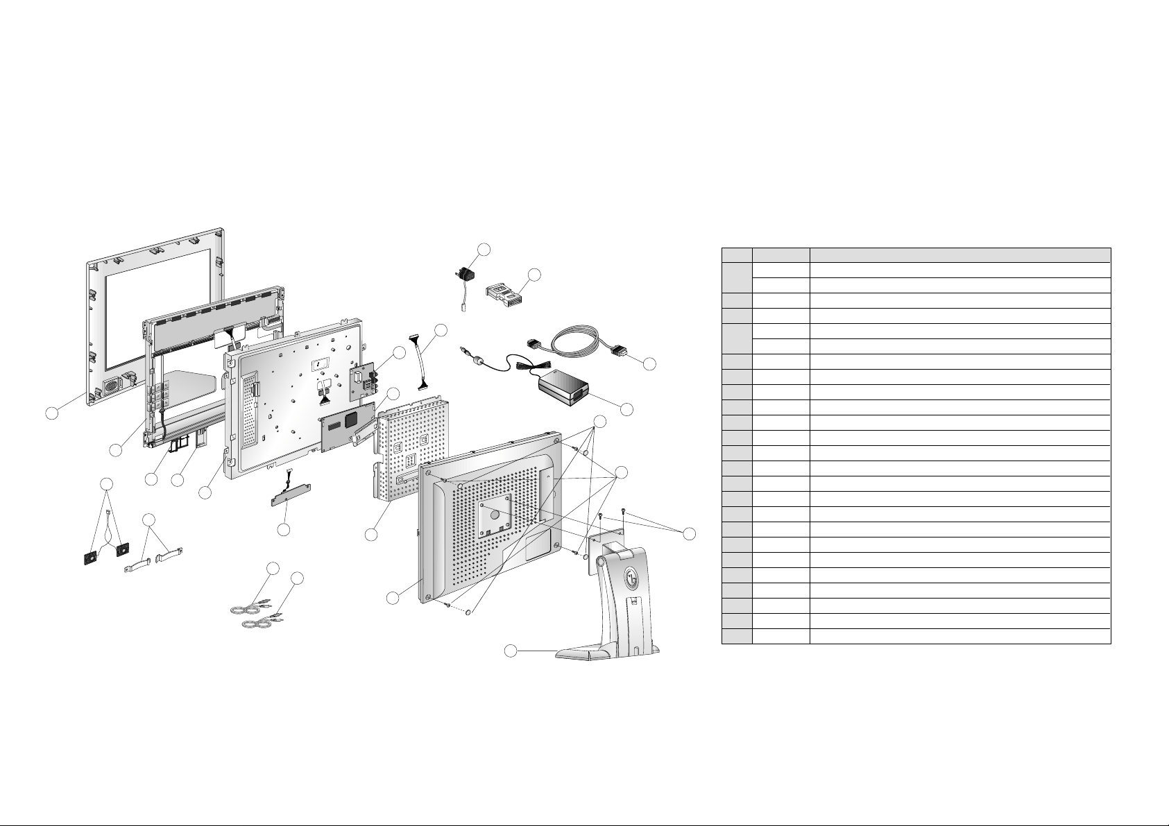
EXPLODED VIEW PARTS LIST
Ref. No.
1
2
3
4
5
6
7
8
9
10
11
12
13
14
15
16
17
18
19
20
21
22
23
Part No.
3091TKL030B
3091TKL030E
6304FTS001A
3809TKL020B
3043TKK057M
3043TKK057Q
6633TZA003G
4951TKS072D
6871TST257A
6871TMT268C
6871TST256A
4951TKS077C
6631T11012N
332-068T
332-105F
6401TZZ025A
4950TKK337A
6634TBZ016A
6866TD9001F
6852TAZ006E
6852TAZ006F
5410TKK015D
381-240A
6634TFZ002A
4810TKK173A
Description
CABINET ASSEMBLY, LM568E BRAND 3090TKL029A ONLY TCO95 LABEL
-For Europe
CABINET ASSEMBLY, LM568E BRAND 3090TKL029A TCO95, SILVER SPRAY
-For Japan
LCD, LTM15C443L TOSHIBA 15.0 INCH XGA(1024 X 768) TFT COLOR W/O INVERTER
BACK COVER ASSEMBLY, LM568E 3808TKL023 ADD ADAPTOR LABEL
TILT SWIVEL ASSEMBLY, LM568E (BUILT-IN SPEAKER) SPRAY -For Europe
TILT SWIVEL ASSEMBLY, LM568E . BOTTOM(BLUE SPRAY) -For Japan
INVERTER ASSEMBLY, SAMSUNG LG1511 LB565C
METAL ASSEMBLY, "FRAME MAIN, LB568"
PWB(PCB) ASSEMBLY, SUB, LM568E SOUND TOTAL BRAND XAGC
PWB(PCB) ASSEMBLY,MAIN, LM568E ATLJC BRAND CL-18 TOTAL
PWB(PCB) ASSEMBLY, SUB, LM568E CONTROL TOTAL BRAND XAGC
METAL ASSEMBLY, "REAR FRAME, LM568(TOSHIBA)"
CONNECTOR ASSEMBLY, 20P H-H 120MM UL20276 LM568E INTERFACE,UNIXTAR
SCREW, PPB+3*10(MSWR/FZMW)
SCREW, PVS+4*10(MSWR/FZMW)
SPEAKER ASSEMBLY, LM568E T401SX154K14 SPEAKER ASSY 1W 4OHM
METAL,FIX SPEAKER (LM568E)
ADAPTER, AC-DC, ADP-36UB DELTA 12V 3.0A FOR LG
SIGNAL CABLE, UL 2990-9C(7.5) DT 1870MM GRAY(85964) LB500 DM
CORD,A/V, AUDIO UL 2851 #28-2C 1500MM QUARTZ KSD
CORD,A/V, A/V DH-1560SP-BL UL 2851 #28 1560MM GRAY(85964)
INSULATION, PVC SHEET LM568E(89483)
ADAPTER, AC, KPR-24 KAWASAKI 125V 15A BLACK -Only Japan
ADAPTER,SIGNAL, LIBERTY ENHANCE MAC 6-DIP -Only Japan
BRACKET, LB565C SUPPOTER INVERTER
EXPLODED VIEW
Page 4
- 6 -
WIRING DIAGRAM
J4
CN2
CN1
J4
J10
J5
J3
Connector Ass’y P/N: 6631T11012N
Page 5
(a)
(a)
(a)
(a)
(a)
(a)
(a)
(a)
- 7 -
DISASSEMBLY
(b)
(b)
(c)
(c)
(c)
(a)
MIC.
IN
AUDIO
IN
MIC.
OUT
(a)
(b)
(b)
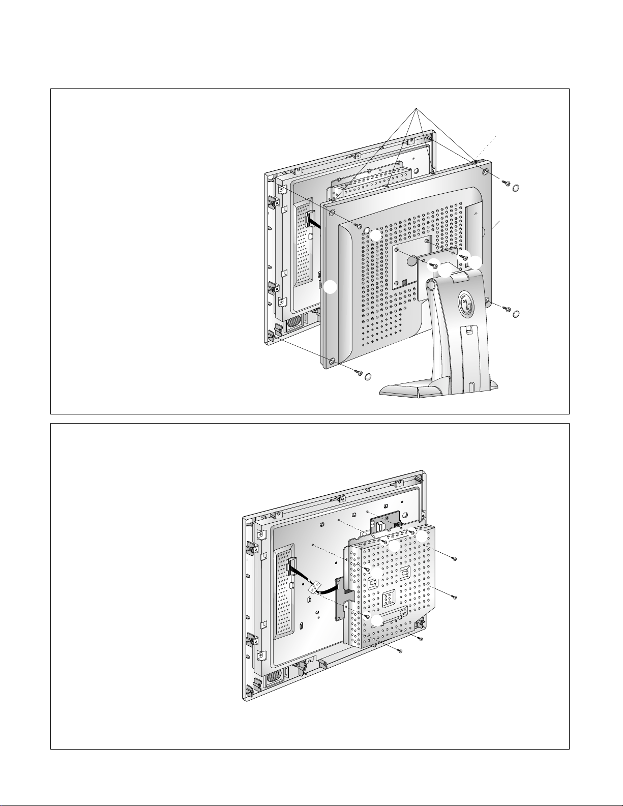
1. TILT/SWIVEL & BACK COVER REMOVAL
(1) Remove two screws (a).
(2) Remove the Tilt/swivel.
(3) Remove four sheets.
(3) Remove four screws (b) from the Back Cover.
(4) Release six latchs (c).
(5) Remove the Back Cover.
2. REAR METAL ASS’Y REMOVAL
(1) Remove eight screws (a).
(2) Remove the Rear Metal Ass’y.
Back Cover
Page 6
- 8 -
4. MAIN FRAME REMOVAL
(1) Remove eight screws (a).
(2) Remove the Main Frame.
5. LCD MODULE REMOVAL
(1) Remove four screws (a).
(2) Separate the LCD Module from the Main Frame.
LCD Module
(d)
(d)
(a)
(b)
(a)
(a)
(b)
(b)
(a)
J4
J5
J10
(a)
(a)
J3
J4
(c)
(c)
(c)
3. MAIN PCB ASS’Y & CONTROL PCB , SOUND ASS’Y,
SPEAKER ASS’Y REMOVAL
(1) Disconnect J4,J5 and J10 from the Main PCB Ass’y.
(2) Remove six screws (a).
(3) Remove the Main PCB Ass’y.
(4) Remove three screws (b).
(5) Disconnect J4 and J3 from the Sound Ass’y
(6) Remove the Sound Ass’y.
(7) Remove three screws (c).
(8) Remove the Control PCB Ass’y.
(9) Remove two screws (d).
(10)
Remove two Metal Fix.
(11)
Remove the Speaker Ass’y
(a)
(a)
(a)
(a)
(a)
(a)
(a)
(a)
(a)
(a)
(a)
(a)
Page 7
- 9 -
CN2
6. INVERTER ASS’Y REMOVAL
(1) Disconnect CN2
(2) Remove two latch (a).
(3) Remove the Inverter Ass’y.
(a)
(a)
Page 8

BLOCK DIAGRAM
- 10 -
Power Part
DC/DC
Converter
(L4973)
12V
ST5V
ST5V
EEPROM
24WC08
ADC/PLL/Scaler
(gmZAN1)
(MICOM)
(MTV212MS64I)
Switch
FDC6325L
Switch
FDC6325L
Schmitt Trigger
(74HCT14)
RGB
H.V
D-
Sub
15P
DDC
Control
DC
Jack
SCL
SDA
CON
10P
Inverter
3.3 VD
3.3 V_PL
Module Power
3.3V
3.3V_PL
3.3VD
ST5V
RGB
3.3V_AD
Regulator
BA033
Regulator
BA033
Regulator
BA033
3.3 V_AD
+3.3V
Headphone
MIC In
MIC Out
Audio In
Audio
Processor
(TDA7449)
Audio Amp
(TDA7496L)
SCLSDA
78 M08
8VA
12V
12V(Audio B/d)
Audio Mute
(Audio B/d)
CON 5P
12V
GND
SCL
SDA
Audio
Mute
12V
Audio Mute
LCD
Interface
20Pin
Connector
(12507WR-20P)
LVDS
(LVDS83)
RIN
RCLK
Regulator
BA033
Hsync2
Vsync2
Hsync2
Vsync2
Hsyncm
Vsyncm
+3.3V
CON 5P
To Audio B/d
Main B/d
Audio B/d
Page 9

DESCRIPTION OF BLOCK DIAGRAM
- 11 -
1. Scaler One chip IC(GMZAN1, U3)
GMZAN1 (U3) is one chip IC which it supports four internal function blocks of Video Amp, PLL,
A/D converter and Video processor.
Video signal (0.7Vp.p) clamped through C44, 45, 191 with matching IC’s proper cut off voltage.
This signal is processed as a proper 8 bit digital signal by U3’s amplifying, phase locking, A/D converting,
and scaling operations.
U3 generates Clock, Horizontal and Vertical sync, Data Enable signals as LCD Panel’s input signals.
2. System Controller (Microprocessor) Circuit.
1) Microprocessor (U4) distinguishes polarity and frequency by calculating horizontal and vertical sync input
from signal source.
2) Microprocessor (U4) carries out power control by sending power-down trigger signal to each IC.
3) Microprocessor (U4) communicates with EEPROM (U1), and GMZAN1 (U3)
through IIC(2 lines) or 6 bit bus line. It makes all devices operated properly.
4) Microprocessor (U4) let User adjust screen by OSD function.
3. DC/ DC Converter.
This circuit supplies DC power for each device needing DC voltage of 3.3VD, 3.3V_AD, 3.3V_PL, Module Power 3.3V
and 5VS.
L4973D5.1(U13) , the DC/DC controller IC converts input 12Vdc into 5VS and 3.3Vdc with peripheral circuit
composed of Inductor (L11), condensing components (ZD5, C72), and Regulators(U2, U7, U24,U30).
MODPWR(3.3V) for LCD module power is switched by U12, switching FET, controlled by Microprocessor.
3.3VD, 3.3V_AD, and 3.3V_PL for GMZAN1 (U3) and 3.3V for LVDS (U9) are switched by U5, switching FET,
controlled by Microprocessor for Power saving.
4. Display Data Transmitter Part (LVDS).
This part transmit digital signal from the Scaler to the receiver of module.
5. Audio Part (TDA7449,TDA7496L)
In This Circuit, Audio Processor(TDA7449) Which is Controlled by Microprocessor(U4) adjust
volume/treble/bass/balance of Audio signal which come from PC.
The Signal come from TDA7449 is amplified by TDA7496L. The final output signal is output through speaker.
Page 10

ADJUSTMENT
- 12 -
220
IBM
Compatible PC
PARALLEL PORT
Power inlet (required)
Power LED
ST Switch
Power Select Switch
(110V/220V)
Control Line
Not used
RS232C
PARALLEL
V-SYNC
POWER
ST
VGS
MONITOR
E
E
V-Sync On/Off Switch
(Switch must be ON.)
F
F
A
A
B
B
C
C
15
10
5
5
69
1
1
1
14
13
25
6
5V
5V
5V
4.7K
4.7K
4.7K
74LS06
74LS06
OFF ON
OFF
ON
11
Video Signal
Generator
24V
AUDIO
DC OUT
MIC.
IN
AUDIO
IN
MIC.
OUT
Figure 1. Cable Connection
All adjustment are thoroughly checked and corrected
when the monitor leaves the factory, but sometimes
several minor adjustment may be required.
Adjustment should be following procedure and after
warming up for a minimum of 10 minutes.
Alignment appliances and tools.
- IBM Compatible PC
- Programmable Signal Generator.
(eg. VG-819 made by Astrodesign Co.)
- E(E)PROM with each mode data saved.
- Alignment Adapter and Software.
1. Adjustment for Factory Preset Mode
1) Run alignment program for LM568E on the IBM
compatible PC.
2) Display cross hatch pattern at Mode 1.
3) Select EEPROM ALL Init command and Enter.
4) Press "Y" key, it will automatically save all FOS data
to EEPROM.
2. Adjustment for White Balance
1) Display color 0,0 pattern at Mode 12.
2) Set External Bright to MAX position and Contrast to
MAX Position.
3) Select PRESET START
→ BIAS CAL command
and Enter.
4) No attempt to manually adjust, BIAS data is automatically adjusted and saved to the EEPROM.
5) Display color 15,0 pattern at Mode 12.
6) Select DRIVE CAL command and Enter.
7) Color 1 (9300K) and Color 2 (6500K) are
automatically adjusted and saved to the EEPROM.
8) Select PRESET EXIT command and Enter.
3. DDC Data Write Procedure
1) Use this procedure only when there is some
probelm on EDID data.
2) Select EEPROM → EDID Write command and
Enter.
3) This will write the EDID data to EEPROM.
Page 11

- 13 -
TROUBLESHOOTING GUIDE
1. NO POWER
CHECK U4.
CHECK
U4 PIN 8 VOLTAGE
(5V) ?
NO
NO POWER
(POWER INDICATOR OFF)
CHECK ADAPTER,
AND FIND OUT
A SHORT POINT
AS OPENING
EACH POWER LINE
CHECK J1’S
VOLTAGE
(12V) ?
NO
CHECK L11
(OPEN CHECK)
CHECK
U5 Voltage
(5V) ?
NO
U13’S PIN11
0V ?
CHECK U13, AND
CHECK 5VA LINE
CHECK IIC LINE
CONNECTION
(U4, U1)
CHECK U3’S VCC,
X-TAL, RESET
IS U13 PIN2
VOLTAGE REPEATED
AS PULSE SHAPE ?
NO
YES
YES
YES
NO
YES
NO PROBLEM
NO
CHECK KEY CONTROL
CONNECTOR ROUTINE
Page 12

- 14 -
2. NO RASTER (OSD IS NOT DISPLAYED) – INVERTER
CHECK MICOM INV
ON/OFF PORT.
J4 PIN5
5V?
NO
NO RASTER
(OSD IS NOT DISPLAYED)
CHECK ADAPTER
J4 PIN10
12V?
NO
1. CONFIRM BRIGHTNESS
OSD CONTRL STATE.
2. CHECK MICOM DIM-ADJ
PORT
J4 PIN1
5V?
NO
REPLACE
INVERTER ASS’Y
CHECK
PULSE AS
CONTACTING SCOPE
PROBE TO CAUTION LABEL.
(CONTACT PROBE TO
CAUTION LABEL.
CAN YOU SEE PULSE
AT YOUR
SCOPE?
NO
REPLACE CCFL LAMP
IN THE LCD MODULE
YES
YES
YES
YES
Page 13

- 15 -
1. CHECK PIN141, 142
SOLDERING CONDITION
2. CHECK X2
3. TROUBLE IN U3
U3
POWER PINS
3.3V?
NO
CHECK U2, U24
U3 PIN141, 142
OSCILLATE AS 14.3M?
NO
CHECK U9’S SOLDERING
CONDITION AND
CHECK CONNECTION LINE
FROM U3 TO J5
NO
TROUBLE IN CABLE
OR LCD MODULE
CHECK U12, U30
J5 PIN1
3.3V?
NO
YES
YES
YES
YES
3. NO RASTER (OSD IS NOT DISPLAYED) – gmZAN1
NO RASTER
(OSD IS NOT DISPLAYED)
U9
PIN31 IS 65MHz CLOCK?
PIN27 IS 48KHz H-SYNC?
PIN28 IS 60Hz V-SYNC?
IS PULSE APPEARED
AT SIGNAL PINS?
Page 14

- 16 -
CHECK U2, U24
U3
POWER PIN
3.3V?
NO
1. CHECK PC
2. CHECK SIGNAL CABLE
& D-SUB CONNECTOR
LINE
CHECK
R,G,B INPUT?
U3 PIN 87, 91, 95
NO
CHECK H-SYNC LINE
(D-SUB→U6 →U3
PIN150)
CHECK
H-SYNC INPUT
U3 PIN 150?
NO
YES
YES
YES
NO RASTER
(OSD IS DISPLAYED)
4. NO RASTER (OSD IS DISPLAYED) – gmZAN1
Page 15

- 17 -
CHECK SPEAKER
CHECK SPEAKER
ASS’Y?
NO
CHECK JACK(J7)
& AUDIO CORD
AUDIO PCB
CHECK INPUT SIGNAL
U3(TDA7449)
PIN7,8?
NO
CHECK MAIN
U3(MICOM)
→AUDIO J3
→U3(TDA7449)
CHECK
IIC LINE
NO
YES
YES
YES
YES
CHECK U3(TDA7449)
CHECK
INPUT SIGNAL
U1(TDA7496L)
PIN4,9?
NO
CHECK U1(TDA7496L)
CHECK
OUTPUT SIGNAL
U1(TDA7496L)
PIN14,17?
NO
NO SOUND
5. NO SOUND
YES
Page 16

SCHEMATIC DIAGRAM
- 31 -
1. GMZAN1
Page 17

- 32 -
2. LVDS
Page 18

- 33 -
3. MICOM
Page 19

- 34 -
4. POWER
Page 20

- 35 -
5. CONNECTOR & JACKS
Page 21

- 36 -
6. AUDIO
Page 22

- 37 -
7. CONTROL KEY
 Loading...