

LG LM-240WU6-SDA1 Service manual
( ● ) Preliminary Specification
( ) Final Specification
LM240WU6
Liquid Crystal Display
Product Specification
SPECIFICATION
FOR
APPROVAL
24.0” WUXGA TFT LCDTitle
BUYER
www.jxlcd.com
www.jxlcd.com
APPROVED BY
/
/
/
APPLE
K29MODEL
SIGNATURE
DATE
*When you obtain standard approval,
please use the above model name without suffix
APPROVED BY
Hans Kim / G.Manager
REVIEWED BY
SY.Park / Manager
PREPARED BY
B.C KIM / Engineer
LG Display Co., Ltd.SUPPLIER
LM240WU6*MODEL
SDA1SUFFIX
SIGNATURE
DATE
Please return 1 copy for your confirmation with
your signature and comments.
Ver. 0.R Sept. 24 . 2008
MNT Products Engineering Dept.
LG Display Co., Ltd.
1/ 36
Product Specification
Contents
LM240WU6
Liquid Crystal Display
ITEMNo
COVER
CONTENTS
RECORD OF REVISIONS
GENERAL DESCRIPTION1
ABSOLUTE MAXIMUM RATINGS2
ELECTRICAL SPECIFICATIONS3
ELECTRICAL CHARACTREISTICS3-1
INTERFACE CONNECTIONS3-2
SIGNAL TIMING SPECIFICATIONS3-3
SIGNAL TIMING WAVEFORMS3-4
COLOR INPUT DATA REFERNECE3-5
POWER SEQUENCE3-6
OPTICAL SFECIFICATIONS4
www.jxlcd.com
www.jxlcd.com
MECHANICAL CHARACTERISTICS5
Page
1
2
4
5
7
8
8
11
14
15
16
17
20
26
RELIABLITY6
INTERNATIONAL STANDARDS7
SAFETY7-1
EMC7-2
PACKING8
DESIGNATION OF LOT MARK8-1
PACKING FORM8-2
PRECAUTIONS9
MOUNTING PRECAUTIONS9-1
OPERATING PRECAUTIONS9-2
ELECTROSTATIC DISCHARGE CONTROL9-3
PRECAUTIONS FOR STRONG LIGHT EXPOSURE9-4
STORAGE9-5
HANDLING PRECAUTIONS FOR PROTECTION FILM9-6
Ver. 0.R Sept. 24 . 2008
29
30
30
30
31
31
31
32
32
32
33
33
33
33
2/ 36
Product Specification
Contents
LM240WU6
Liquid Crystal Display
ITEMNo
EDID DATA10
EDID DATA10-1
EDID READ/WRITE PROTOCOL10-2
www.jxlcd.com
www.jxlcd.com
Page
34
34
36
Ver. 0.R Sept. 24 . 2008
3/ 36

Product Specification
RECORD OF REVISIONS
LM240WU6
Liquid Crystal Display
Revision
No
DescriptionPageRevision Date
First Draft(Preliminary)-Jan. 9. 20080.0
Table 2-1 DP Logic Voltage added6Jan. 14. 20080.0B
Table 3 CN_SIG pin mapping fixed8
9
9
10
11
www.jxlcd.com
www.jxlcd.com
20pin CNT P/N correction
Table 2-1-2 DP Logic Input Current added (Sleep Mode)7Feb.13.20080.0C
Table 2-1-2 DP Logic Input Current added (Off Mode)7
30pin CNT P/N correction
20pin CNT P/N correction
3pin CNT P/N & pin mapping correction
Power Sequence correction14
EDID Data added30
EDID Read/Write Protocol added32Feb.15.20080.0D
Update Drawings23,24March.26.20080.0E
Block diagram delete optical sensor2
Table 2-1-1 DP Logic Input Current & Power Consumption correction6
Optical sensor Connector delete11
Power sequence T8, T12 change15
EDID Data correction30
Power Sequence, EDID Read / Write added16March.31.20080.0F
State Machine add18April.11.20080.0G
Sleep mode, off mode Power8
T13 add16
EDID read power sequence change17
Timing change13April.28.20080.0H
Power sequence change16, 17
Update Weight5,25
LED Bar Specification update9
Ver. 0.R Sept. 24 . 2008
4/ 36
Product Specification
Signal timing specification change (156MHz→154MHz)14May. 9. 20080.0I
EDID change35
Stand by mode max power update9
LM240WU6
Liquid Crystal Display
DescriptionPageRevision DateRevision No
27,28
8May. 19. 20080.0J
17
27May. 28.2008
34,35,3
6
www.jxlcd.com
www.jxlcd.com
Update Drawing
Optical spec. update20
Add Vdpogic input voltage7
Power Suppy Input Current update
Power Consumption update6, 8
Power Sequence Change.
(T2:min 0.01m0, T6:min 0.01m0)
Update Drawing
Update EDID ( Check Sum : 22 03 )
Luminance change 350=>330nit6June.24.20080.0K
HDCP key information add
Luminance spec change20
Box size31
Drawing update18, 28July. 22. 20080.0L
T3 min spec change (1ms→0.01ms), Add T10, T1117
Delete AUX-power pin function11
Power consumption update6
T8 min spec change (1000ms → 250ms). T9 min(0 → 200ms)17Aug.8.20080.0M
Drawing update28
Optical spec(Luminance, color cordinate), power consumption update6,20
Aging Time change(30min 120min)20
Power sequence change17Aug.12.20080.0N
Correct the name of 20pin, 30pin CNT11, 12Aug.14.20080.0O
Gray Scale update.25Aug.22.20080.0P
Power consumption update6,10Sep.09.2008
Life time update10
Delete equivalent connector11,12Sep.19.20080.0Q
Power sequence change17
Power sequence change17Sep.24.20080.0R
Ver. 0.R Sept. 24 . 2008
5/ 36
LM240WU6
Liquid Crystal Display
Product Specification
1. General Description
LM240WU6 is a Color Active Matrix Liquid Crystal Display with Light Emitting Diode ( White LED) backlight
system without LED driver. The matrix employs a-Si Thin Film Transistor as the active element.
It is a transmissive type display operating in the normally black mode. It has a 24inch diagonally measured
active display area with WUXGA resolution (1200 vertical by 1920 horizontal pixel array)
Each pixel is divided into Red, Green and Blue sub-pixels or dots which are arranged in vertical stripes.
Gray scale or the brightness of the sub-pixel color is determined with a 8-bit gray scale signal for each dot,
thus, presenting a palette of more than 16,7M(True) colors.
It has been designed to apply the 8Bit 2Lane Display port interface.
It is intended to support displays where high brightness, super wide viewing angle,
high color saturation, and high color are important.
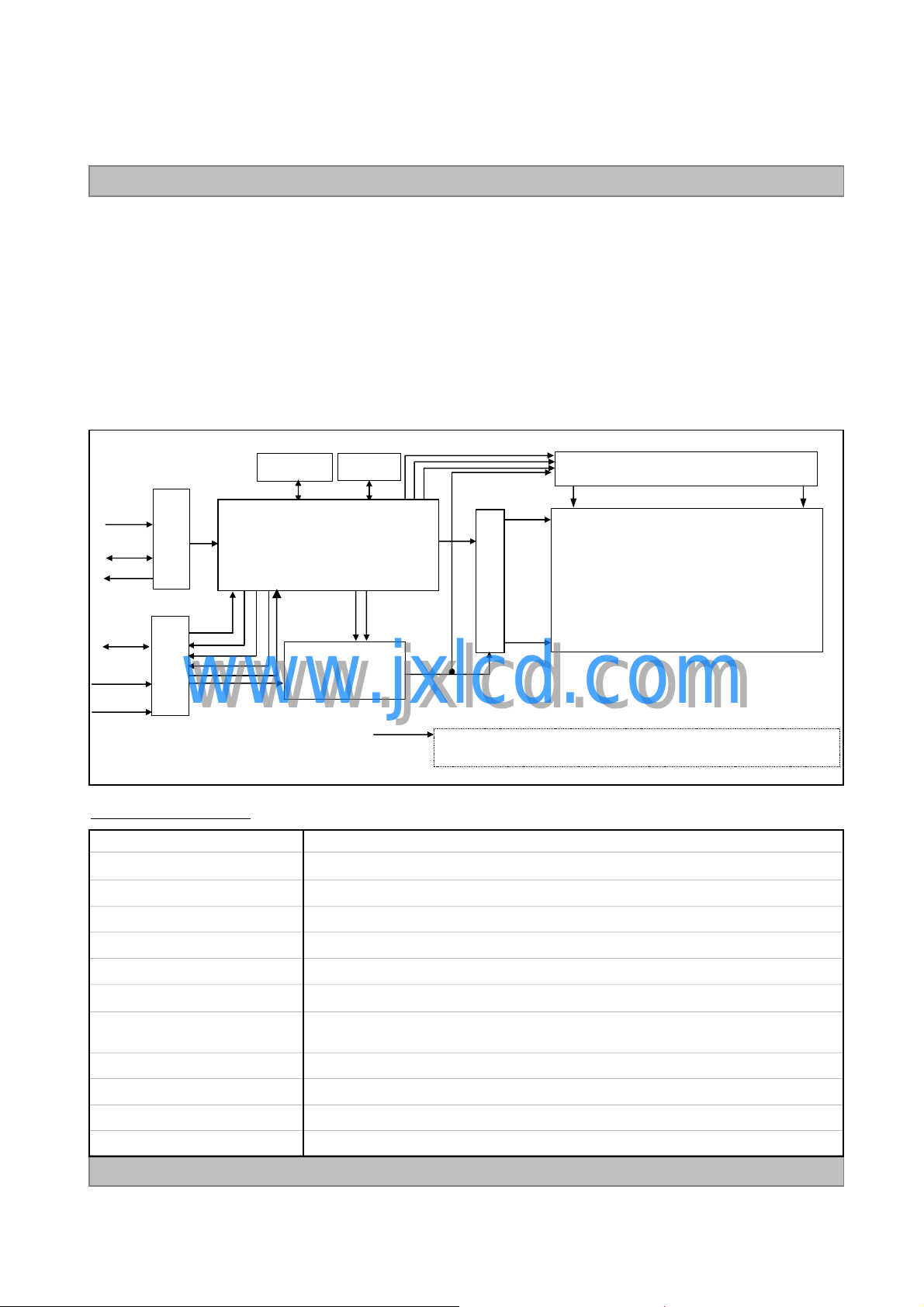
Main Link
2 port
HPD
CN1
(30pin)
CN2
www.jxlcd.com
(20pin)
www.jxlcd.com
AUX CH
DP function
Logic Power
3.3V
LCD Power
12 V
General Features
Flash
memory
SPI
Timing
Controller
Logic Power
3.3V
Power
Circuit
24.0 inches(60.96cm) diagonalActive Screen Size
546.4(H) x 361.6(V) x 18.3(D) mm(Typ.) <- W/O LED DriverOutline Dimension
0.270 mm x 0.270 mmPixel Pitch
1920 horiz. By 1200 vert. Pixels RGB stripes arrangementPixel Format
8-bit, 16,777,216 colorsColor Depth
320 cd/m
EEPR
I2C
Block
OM
Power
Enable
(DPM,Video On)
Vled 6ch
2
( 5 points Avg.)Luminance, White
Mini-LVDS (RGB)
Gate Driver Circuit
G1
G1200
Source Driver Circuit
S1 S1920
TFT - LCD Panel
(1920 × RGB × 1200 pixels)
B/L System (White LED)
View Angle Free (R/L 178(Typ.), U/D 178(Typ.))Viewing Angle(CR>10)
Power Consumption
Ver. 0.R Sept. 24 . 2008
Total 71.17 Watt (Max.)
, Max 65.05 Watt_ Duty 92% of DC356mA_ w/o driver)
@V
(6.12 Watt
3500g (typ.) 3700g (Max.)Weight
Transmissive mode, normally blackDisplay Operating Mode
Hard coating(2H), Glare(Low Reflection treatment of the front polarizer)Surface Treatment
HDCP key implemented in Tcon (DP621)HDCP
LCD
6/ 36
LM240WU6
Liquid Crystal Display
Product Specification
2. Absolute Maximum Ratings
The following are maximum values which, if exceeded, may cause faulty operation or damage to the unit.
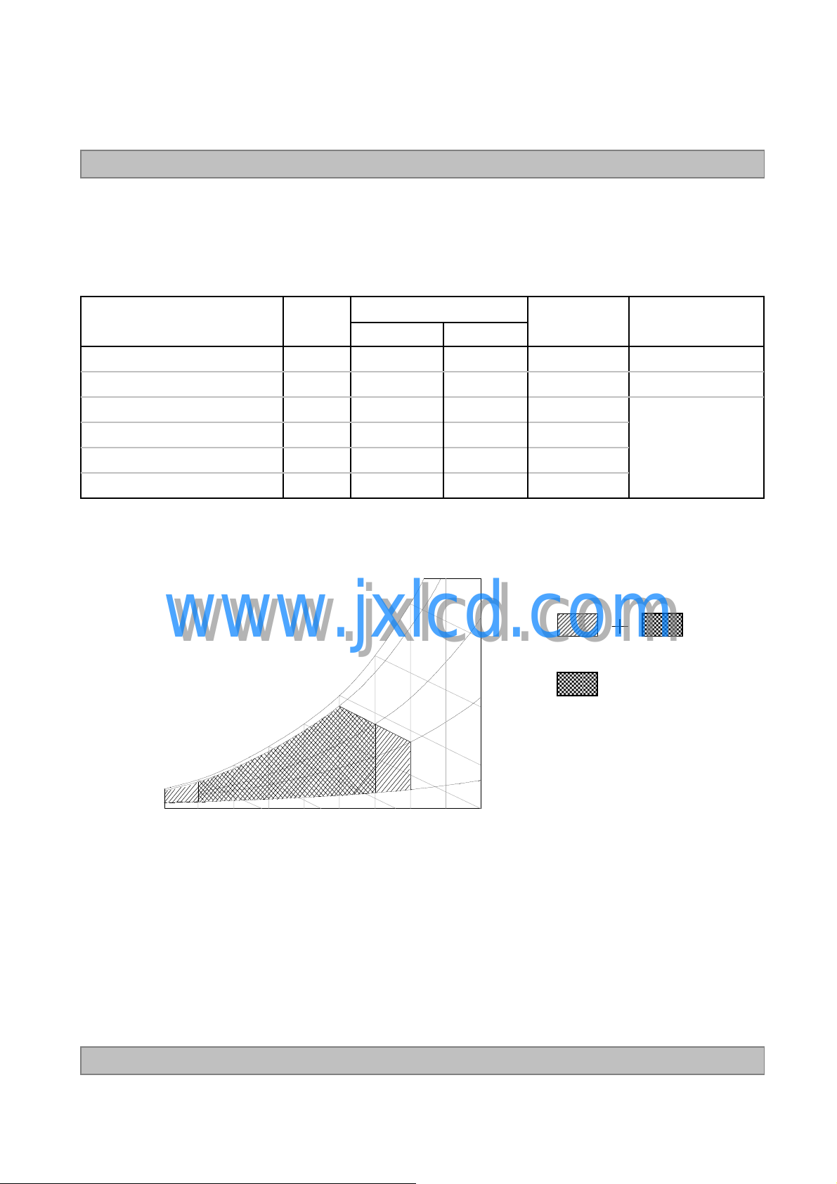
Table 1. ABSOLUTE MAXIMUM RATINGS
Parameter Notes
Power Input Voltage
Power Input Voltage
Operating Temperature
Storage Temperature
Operating Ambient Humidity
Storage Humidity
Note : 1. Temperature and relative humidity range are shown in the figure below.
Wet bulb temperature should be 39 °C Max, and no condensation of water.
www.jxlcd.com
www.jxlcd.com
Wet Bulb
Temperature [C]
10
0
Symbol
LCD
DPLOGIC
OP
ST
OP
ST
50
40
30
20
Values
MaxMin
500T
60-20T
90%
60
60%
40%
Humidity [(%)RH]
10%
Units
Vdc14-0.3V
Vdc4-0.5V
°C
°C
%RH9010H
%RH9010H
at 25 2°C
at 25 2°C
1
Storage
Operation
10 20 30 40 50 60 70 800-20
Dry Bulb Temperature [C]
Ver. 0.R Sept. 24 . 2008
7/ 36
LM240WU6
Liquid Crystal Display
Product Specification
3. Electrical Specifications
3-1. Electrical Characteristics
It requires two power inputs. One is employed to power the LCD electronics and to drive the TFT array and
liquid crystal. The second input power for the DP Rx.
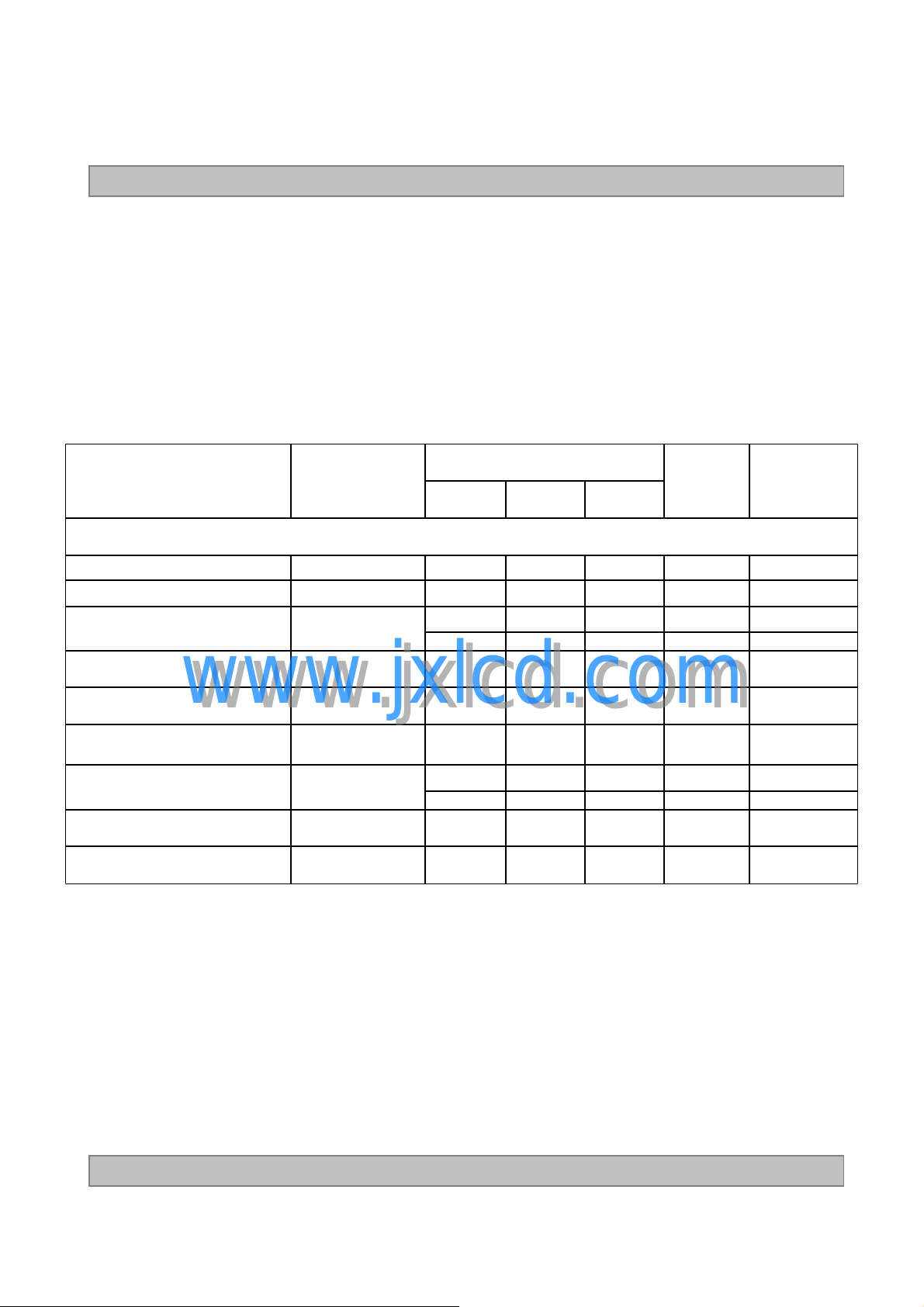
Table 2-1-1. ELECTRICAL CHARACTERISTICS (Normal Mode)
Values
SymbolParameter
MaxTypMin
MODULE :
Vdc12.612.011.4VLCDPower Supply Input voltage
mVp-p400-VdRFPermissive Power Input Ripple
ILCDPower Supply Input Current
NotesUnit
1mA403350297
2mA587510433
www.jxlcd.com
www.jxlcd.com
Vdc3.473.33.13VCC_DPLOGICDP Logic Input Voltage
I_DPLOGICDP Logic Input Current
Watt1.0P_DPLOGICDP Logic Power Consumption
2Watt7.046.12-PLCDPower Consumption
3A3.0--IRUSH_VLCDRush Current
1mA300
2mA300
3A1.0--IRUSH_DPLOGICDP Rush Current
Ver. 0.R Sept. 24 . 2008
8/ 36
Product Specification
Table 2-1-2. ELECTRICAL CHARACTERISTICS (Sleep Mode)
Values
SymbolParameter
Table 2-1-3. ELECTRICAL CHARACTERISTICS (Off Mode)
LM240WU6
Liquid Crystal Display
NotesUnit
MaxTypMin
mA6024-I_DPLOGICDP Logic Input Current
mW20080-P_DPLOGICDP Logic Power Consumption
Values
SymbolParameter
www.jxlcd.com
www.jxlcd.com
Note :
1. The specified current and power consumption are under the V
whereas mosaic pattern(8 x 6) is displayed and f
2. The current is specified at the maximum current pattern.
3. The duration of rush current is about 2ms and rising time of power Input is 1ms(min.).
White : 255Gray
Black : 0Gray
is the frame frequency.
V
LCD
Maximum current pattern
MaxTypMin
mA3021-I_DPLOGICDP Logic Input Current
mW10070-P_DPLOGICDP Logic Power Consumption
=12.0V, 25 2°C,fV=60Hz condition
NotesUnit
Mosaic Pattern(8 x 6)
Ver. 0.R Sept. 24 . 2008
White Pattern
9/ 36
Product Specification
Table 2-2. LED Bar ELECTRICAL CHARACTERISTICS
LM240WU6
Liquid Crystal Display
LED Bar Voltage
LED String Power
Power Consumption
LED driver design guide
: The design of the LED driver must have specifications for the LED in LCD Assembly.
The performance of the LED in LCM, for example life time or brightness, is extremely influenced by
the characteristics of the LED driver.
So all the parameters of an LED driver should be carefully designed and output current should be
Constant current control.
www.jxlcd.com
www.jxlcd.com
When you design or order the LED driver, please make sure unwanted lighting caused by
the mismatch of the LED and the LED driver (no lighting, flicker, etc) never occurs.
When you confirm it, the LCD module should be operated in the same condition as installed in
your instrument.
Bar
Bar
ConditionSymbolParameter
Values
Max.Typ.Min.
s
150--TjLED Junction Temperature
Unit
℃
Notes
1,7LED :
2,7mA700350-IsLED String Current
3,7V73.2-60VsLED String Voltage
3,7V198.6--V
4,7Watt25.62-21P
4,6,7Watt69.51-63P
5,7Hrs--39,000LED_LTLED Life Time
7
1. Specified values are for a single LED bar.
2. The specified current is input LED chip 100% duty current.
3. The specified voltage is input LED string and Bar voltage at typical 350 mA 100% duty current.
4. The specified power consumption is input LED bar power consumption at typical 350 mA 100% duty current.
5. The life is determined as the time at which luminance of the LED is 50% compared to that of initial
value at the typical LED current on condition of continuous operating at 25 2°C.
6. The LED bar power consumption shown above does not include loss of external driver.
The used LED bar current is the LED typical current.
Min Power Consumption is calculated with PBar = Vs x Is x Nstring
Max Power Consumption is calculated with Pbar = Vbar x Is
7. LED operating DC Forward Current and Junction Temperature must not exceed LED Max Ratings.
Ver. 0.R Sept. 24 . 2008
10 / 36
Product Specification
3-2. Interface Connections
3-2-1. LCD Module
- LCD Connector(CN1). : KDF71G-30S-1H(500) (manufactured by Hirose)
The pin configuration for the 30 pin connector is shown in the table below.
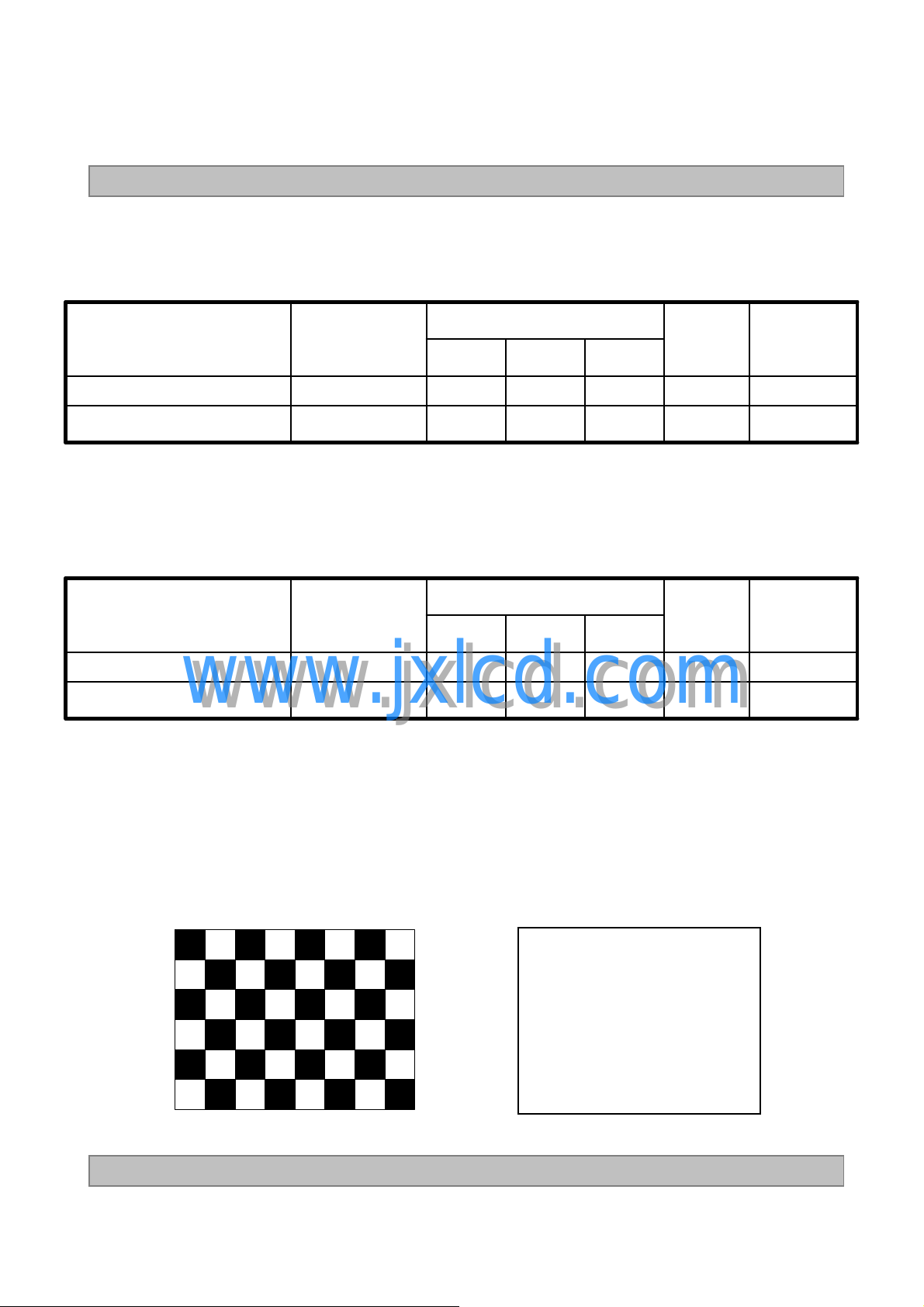
Table 3 MODULE CONNECTOR(CN_SIG) PIN CONFIGURATION
LM240WU6
Liquid Crystal Display
DescriptionSymbolPin No.
1
4
5
VSYNC
H_GND3
AUX_CH N
H_GND6
Lane0P7
www.jxlcd.com
Lane0N8
www.jxlcd.com
H_GND9
Lane1N11
H_GND12
Vertical Sync for signal Checking
ReservedN/C2
High Speed Ground for Auxiliary
Channel
Component Signal for Auxiliary
Channel
True Signal for Auxiliary ChannelAUX_CH P
High Speed Ground for Main
Link 0
True Signal for Main Link 0
Component Signal for Main Link 0
High Speed Ground for Main
Link 1
True Signal for Main Link 1Lane1P10
Component Signal for Main Link 1
High Speed Ground for Main
Link 2
Pin No.
16
17
18
19
20
21
22
23
24
25
26
27
Symbol
Lane3P
Lane3N
H_GND
AUX2
AUX1
HPD
GND
GND
GND
GND
VLCD
VLCD
True Signal for Main Link 3
Component Signal for Main Link 3
High Speed Ground
LCD vender use / No Connection
LCD vender use / No Connection
Hot Plug Detect Signal
GND for main power
GND for main power
GND for main power
GND for main power
12V for LCM main power
12V for LCM main power
Description
True Signal for Main Link 2Lane2P13
Lane2N14
H_GND15
Notes : 1. Connector
2.1 Connector(Receptacle) : KDF71G-30S-1H(500) (Hirose)
2.2 Mating Connector(Plug) : FI-X30HL(JAE).
Ver. 0.R Sept. 24 . 2008
Component Signal for Main Link 2
High Speed Ground for Main
Link 3
28
29
30
VLCD
VLCD
DP_logic
12V for LCM main power
12V for LCM main power
3.3V for DP Rx power
11 / 36
 Loading...