

LG LM-240WU4-SLB3 Service manual
( ●●●● ) Preliminary Specification
SUFFIX
SLB3
( ) Final Specification
Liquid Crystal Display
LM240WU4
Product Specification
SPECIFICATION
FOR
APPROVAL
24.0” WUXGA TFT LCDTitle
BUYER
MODEL
APPROVED BY
www.jxlcd.com
www.jxlcd.com
Please return 1 copy for your confirmation with
/
/
/
your signature and comments.
General
SIGNATURE
DATE
SUPPLIER LG Display Co., Ltd.
*MODEL LM240WU4
*When you obtain standard approval,
please use the above model name without suffix
APPROVED BY
J.H Park / G.Manager
REVIEWED BY
J.Y LEE / Manager [C]
K.H MOON / Manager [M]
G.T KIM / Manager [P]
PREPARED BY
S.J Lee / Engineer
MNT Products Engineering Dept.
LG Display Co., Ltd.
SIGNATURE
DATE
Ver. 0.0 Aug. 5. 2010
1 / 33
Datasheet pdf - http://www.DataSheet4U.net/
Liquid Crystal Display
3-5
15
3-5
15
www.DataSheet.co.kr
Datasheet pdf - http://www.DataSheet4U.net/
LM240WU4
Product Specification
Contents
No ITEM Page
COVER
CONTENTS
RECORD OF REVISIONS
GENERAL DESCRIPTION
1
ABSOLUTE MAXIMUM RATINGS
2
ELECTRICAL SPECIFICATIONS
3
ELECTRICAL CHARACTREISTICS
3-1
INTERFACE CONNECTIONS
3-2
SIGNAL TIMING SPECIFICATIONS
3-3
SIGNAL TIMING WAVEFORMS
3-4
COLOR INPUT DATA REFERNECE
POWER SEQUENCE
3-6
POWER SEQUENCE FOR INVERTER
3-7
www.jxlcd.com
www.jxlcd.com
OPTICAL SFECIFICATIONS
4
MECHANICAL CHARACTERISTICS
5
RELIABLITY
6
7 INTERNATIONAL STANDARDS
7-1 SAFETY
7-2 EMC
7-3 ENVIRONMENT
8 PACKING
8-1 DESIGNATION OF LOT MARK
8-2 PACKING FORM
8-3 PALLET FORM 31
9 PRECAUTIONS 32
1
2
3
4
5
6
6
8
13
14
16
17
18
24
27
28
28
28
28
29
29
30
Ver. 0.0 Aug. 5. 2010
2 / 33
Product Specification
www.DataSheet.co.kr
Datasheet pdf - http://www.DataSheet4U.net/
RECORD OF REVISIONS
Liquid Crystal Display
LM240WU4
Revision
No
0.0 Aug. 5. 2010 - First Draft(Preliminary)
www.jxlcd.com
www.jxlcd.com
Revision Date Page Description
Ver. 0.0 Aug. 5. 2010
3 / 33
Liquid Crystal Display
Gate Driver Circuit
G1200
Gate Driver Circuit
www.DataSheet.co.kr
Datasheet pdf - http://www.DataSheet4U.net/
LM240WU4
Product Specification
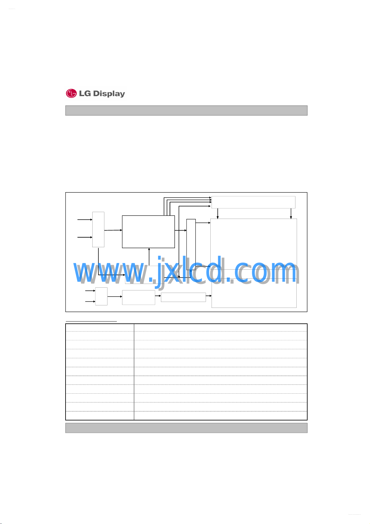
1. General Description
LM240WU4 is a Color Active Matrix Liquid Crystal Display with an integral Cold Cathode Fluorescent
Lamp(CCFL) backlight system. The matrix employs a-Si Thin Film Transistor as the active element.
It is a transmissive type display operating in the normally black mode. It has a 24inch diagonally measured
ac t i ve di s p lay ar e a with W U XGA re s olut i o n (120 0 v e rtica l b y 1920 ho r izont a l pixe l a r ray)
Each pixel is divided into Red, Green and Blue sub-pixels or dots which are arranged in vertical stripes.
Gray scale or the brightness of the sub-pixel color is determined with a 10-bit gray scale signal for each dot,
thus, presenting a palette of more than 1.07B colors.
It has been designed to apply the 10Bit 2 port LVDS interface.
It is i nte n d e d t o s u p po r t d i s p l ay s wh e r e h i g h b r i g h t n e ss , s u p e r w i d e v i e w in g a ngl e ,
high color saturation, and high color are important.
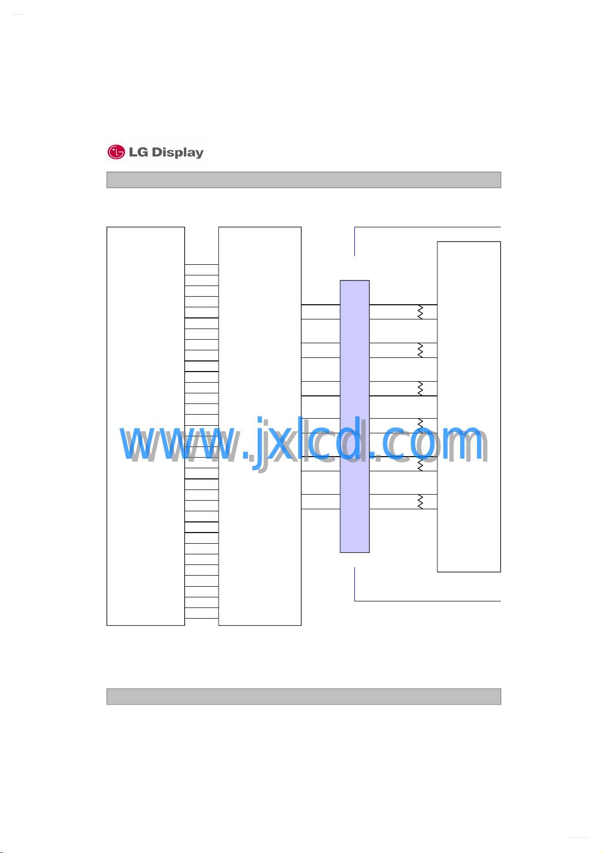
RGB
LVDS
2port
CN1
(51pin)
+12.0V
+12.0V
www.jxlcd.com
www.jxlcd.com
+24.0V
CN2
GND
(14Pin)
Timing
Controller
Power Circuit
Block
Inverter
Block
2pin x 7CNs (High)
G1
Source Driver Circuit
S1 S1920
TFT - LCD Panel
(1920 × RGB × 1200 pixels)
Back light Assembly
(U-Shape 7CCFL)
General Features
Active Screen Size 24.1 inches(61.13cm) diagonal
Outline Dimension 546.4(H) x 352.0(V) x 40.3(D) mm (Typ.)
Pixel Pitch 0.270 mm x 0.270 mm
Pixel Format 1920 horiz. By 1200 vert. Pixels RGB stripes arrangement
Color Depth 8-bit + A-FRC, 1,073,741,824 colors
Luminance, White 400 cd/m
Viewing Angle(CR>10) View Angle Free (R/L 178(Typ.), U/D 178(Typ.))
Power Consumption Total TBD Watt (Typ.) ( TBD Watt @VLCD, 72.0 Watt@V
Weight 2740 g (typ.)
Display Operating Mode Transmissive mode, normally black
Surface Treatment Hard coating(3H), Anti-glare treatment of the front polarizer
2
( Center 1 points)
DDB
)
Ver. 0.0 Aug. 5. 2010
4 / 33
Liquid Crystal Display
www.DataSheet.co.kr
Datasheet pdf - http://www.DataSheet4U.net/
LM240WU4
Product Specification
2. Absolute Maximum Ratings
The following are maximum values which, if exceeded, may cause faulty operation or damage to the unit.
Table 1. ABSOLUTE MAXIMUM RATINGS
Parameter Symbol
Power Input Voltage
Operating Temperature
Storage Temperature
Operating Ambient Humidity
Storage Humidity
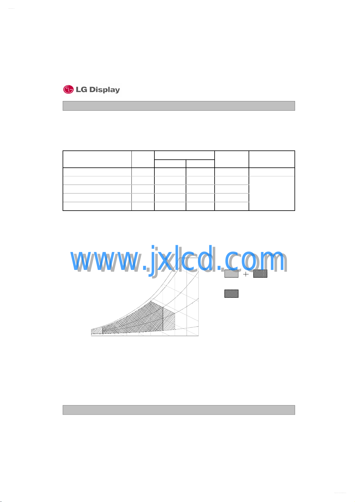
Note : 1. Temperature and relative humidity range are shown in the figure below.
Note : 2. Maximum Storage Humidity is up to 40℃, 70% RH only for 4 corner light leakage Mura.
www.jxlcd.com
Wet bulb temperature should be 39 °C Max, and no condensation of water.
www.jxlcd.com
Wet Bulb
Temperature [C]
10
0
VLCD 8 14 Vdc at 25 ± 2°C
TOP 0 50
TST -20 60
HOP 10 90 %RH
HST 10 90 %RH
50
40
30
20
Values
Min Max
90%
60
60%
40%
10%
Units Notes
°C
°C
Storage
Operation
Humidity [(%)RH]
1, 2
10 20 30 40 50 60 70 800-20
Dry Bulb Temperature [C]
Ver. 0.0 Aug. 5. 2010
5 / 33
Liquid Crystal Display
www.DataSheet.co.kr
Datasheet pdf - http://www.DataSheet4U.net/
LM240WU4
Product Specification
3. Electrical Specifications
3-1. Electrical Characteristics
It requires two power inputs. One is employed to power the LCD electronics and to drive the TFT array and
liquid crystal. The second input power for the CCFL, is typically generated by an inverter. The inverter is an
external unit to the LCDs.
Table 2-1. ELECTRICAL CHARACTERISTICS
Parameter Symbol
MODULE :
Power Supply Input Voltage VLCD 11.4 12.0 12.6 Vdc
Permissive Power Input Ripple VRF 400 mVp-p 1
Power Supply Input Current ILCD
Power Consumption
Rush current IRUSH - - 3.0 A 4
PLCD TYP - TBD TBD Watt 2
PLCD MAX - TBD TBD Watt 2
Min Typ Max
- TBD TBD mA 2
- TBD TBD mA 3
Values
Unit Notes
Note :
www.jxlcd.com
1. Permissive power ripple should be measured under V
www.jxlcd.com
time, we recommend the bandwidth configuration of oscilloscope is to be under 20Mhz.
2. The specified current and power consumption are under the V
whereas mosaic pattern(8 x 6) is displayed and fVis the frame frequency.
3. The current is specified at the maximum current pattern.
4. The duration of rush current is about 2ms and rising time of power Input is 1ms(min.).
White Pattern
< Permissive Power Input Ripple (V
Ver. 0.0 Aug. 5. 2010
=12.0V, 25 ± 2°C,fV=60Hz condition and At that
LCD
=12.0V, 25 ± 2°C,fV=60Hz condition
LCD
Black Pattern
=12.0V, 25 ± 2°C,fV=60Hz) >
LCD
6 / 33
Product Specification
Input Current
I
VBR= 3.3V
-
3.0
3.5A2
www.DataSheet.co.kr
Datasheet pdf - http://www.DataSheet4U.net/
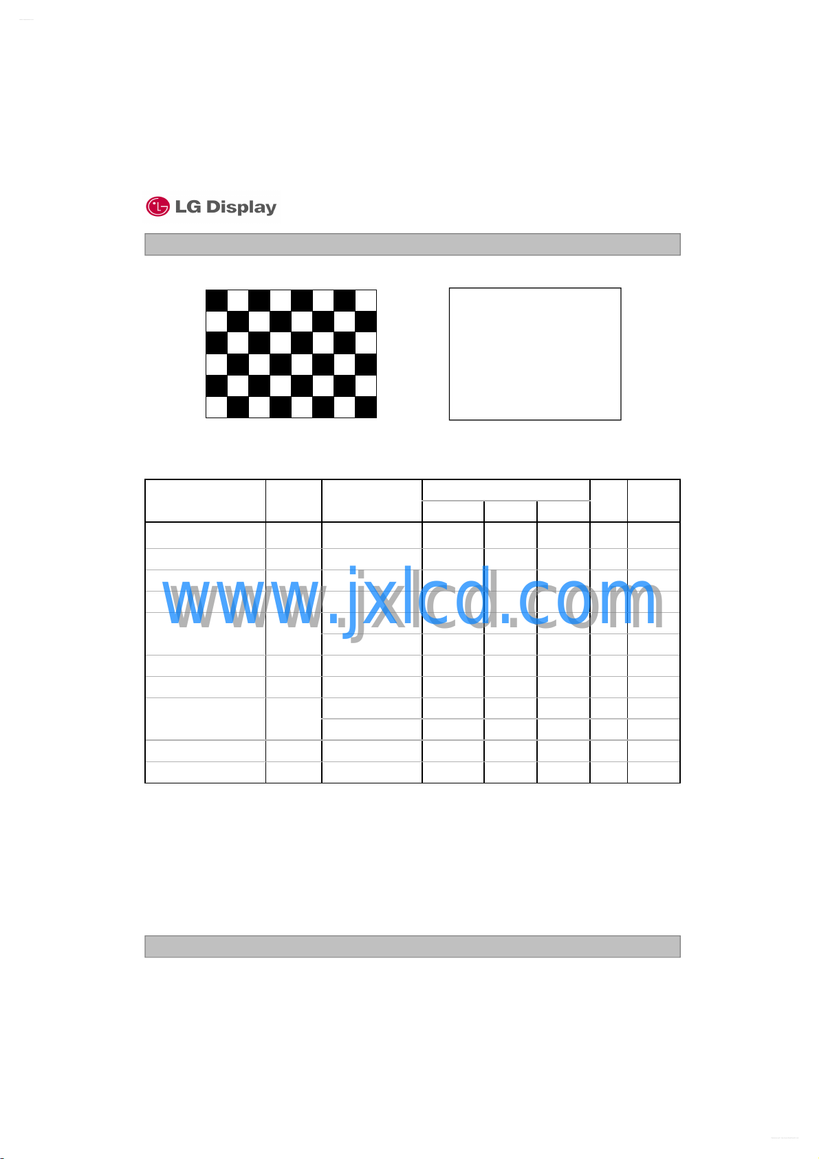
Typical current pattern
(White : 255Gray, Black : 0Gray)
Liquid Crystal Display
LM240WU4
Maximum current pattern
Mosaic Pattern(8 x 6)
< Power consumption (V
Table 2-2. INVERTER ELECTRICAL CHARACTERISTICS
Parameter Symbol Condition
Inverter :
Input Voltage V
Input Power P
www.jxlcd.com
www.jxlcd.com
B/L on/off control V
Brightness Adj V
PWM Frequency F
Pulse Duty Level
(PWM)
LAMP :
Life time
Notes :
1. The input voltage ripple is limited below 400mVp-p.
2. The specified current and power consumption are under the typical supply Input voltage, 24V.
3. LGD recommend that PWM Freq. Is synchronized with three times harmonic of Vsync signal of system
4. The life is determined as the time at which luminance of the lamp is 50% compared to that of initial
value at the typical lamp current on condition of continuous operating at 25 ± 2°C.
5. Electrical characteristics are determined after the unit has been ‘ON’ and stable for approximately
30min in a dark environment at 25 °C± 2°C.
6. In case of the difference in measured values due to the difference
of measuring device was found, correlated value will be used after discussions between both parties.
Ver. 0.0 Aug. 5. 2010
DDB
DDB
B
ON/OFF
BR
b
V
BR
VBR= 3.3V
Lamp ON = High
Lamp OFF =Low
Ext. PWM
High Level
Low Level
=12.0V, 25 ± 2°C,fV=60Hz) >
LCD
Min. Typ. Max.
21.6 24.0 26.4 V 1
-0.3 - 0.8 V
40,000 Hrs 4
White Pattern
Values
- 72.0 84.0 Watt 2
2.5 - 5.0 V
30 100 % On Duty
180 Hz 3
2.0 - 5.0 V
0 - 0.8 V
Unit Notes
7 / 33
.
Liquid Crystal Display
13
RO0P
39
RE3P
www.DataSheet.co.kr
Datasheet pdf - http://www.DataSheet4U.net/
LM240WU4
Product Specification
3-2. Interface Connections
3-2-1. LCD Module
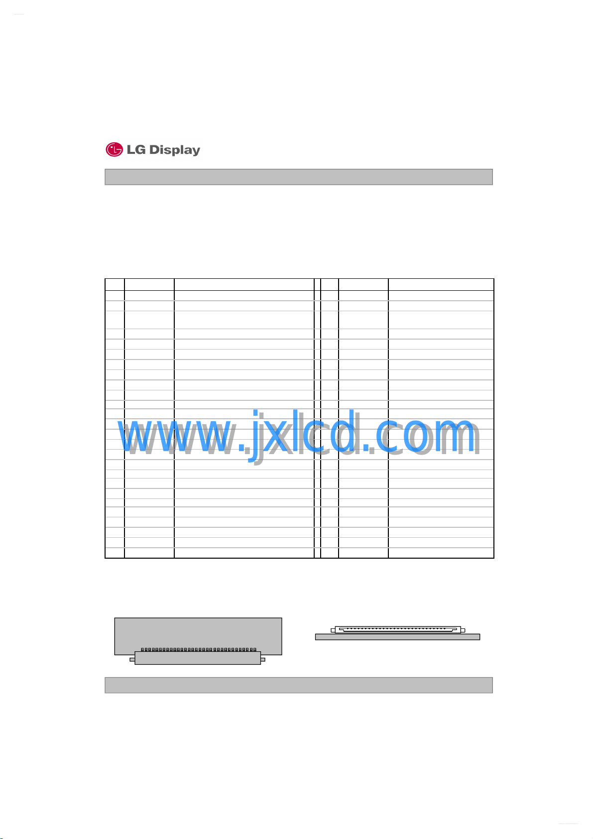
- LCD Connector(CN1). : FI-RE51S-HF (Manufactured by JAE) or equivalent
- Mating Connector: FI-RE51HL (Manufactured by JAE) or equivalent
Table 3 MODULE CONNECTOR(CN1) PIN CONFIGURATION
No Symbol Description No Symbol Description
1
GND
2
3
4
5
6
7
8
9
10
11 GND
12 RO0N
14 RO1N
15
16 RO2N
17 RO2P
18 GND
19 ROCLKN
20
21 GND
22 RO3N
23 RO3P
24 RO4N
25 RO4P
26
NC
ODC ON
NC
NC
NC
NC
GND
NC NC
GND
RO1P
www.jxlcd.com
www.jxlcd.com
ROCLKP
GND
Ground
Reserved
ODC ON/OFF Control
(H:ODC ON, L:ODC OFF, Not Fixed)
(I2C DATA Interface)
(I2C CLK Interface)
Reserved
Reserved
Ground
Ground
Ground
FIRST CHANNEL 0FIRST CHANNEL 0+
FIRST CHANNEL 1FIRST CHANNEL 1+
FIRST CHANNEL 2FIRST CHANNEL 2+
Ground
FIRST CLOCK CHANNEL CFIRST CLOCK CHANNEL C+
Ground
FIRST CHANNEL 3FIRST CHANNEL 3+
FIRST CHANNEL 4FIRST CHANNEL 4+
Ground
27
28 RE0N
29 RE0P
30 RE1N
31 RE1P
32 RE2N
33 RE2P
34
35 RECLKN
36 RECLKP
37 GND
38 RE3N
40 RE4N
41 RE4P
42
43
44
45
46
47
48
49
50
51
GND
GND
GND
GND
GND Ground
GND
NC NC
NC NC
VLCD Power Supply +12.0V
VLCD Power Supply +12.0V
VLCD Power Supply +12.0V
VLCD Power Supply +12.0V
- - -
Note : 1. All GND(ground) pins should be connected together and should also be connected to the LCD’s
metal frame.
2. All VLCD (power input) pins should be connected together.
3. Input Level of LVDS signal is based on the EIA 664 Standard.
User Connector Diagram
#1 #51
Ground
SECOND CHANNEL 0-
SECOND CHANNEL 0+
SECOND CHANNEL 1SECOND CHANNEL 1+
SECOND CHANNEL 2SECOND CHANNEL 2+
Ground
SECOND CLOCK CHANNEL CSECOND CLOCK CHANNEL C+
Ground
SECOND CHANNEL 3SECOND CHANNEL 3+
SECOND CHANNEL 4SECOND CHANNEL 4+
Ground
Ground
Ground
#1 #51
Ver. 0.0 Aug. 5. 2010
Rear view of LCM
8 / 33
Product Specification
GREEN5
46
100Ω
22
www.DataSheet.co.kr
Datasheet pdf - http://www.DataSheet4U.net/
Table 4. REQUIRED SIGNAL ASSIGNMENT FOR LVDS TRANSMITTER
Liquid Crystal Display
LM240WU4
Host System
30 Bit
RED0
RED1
RED2
RED3
RED4
RED5
RED6
RED7
RED8
RED9
GREEN0
GREEN1
GREEN2
GREEN3
GREEN4
GREEN6
www.jxlcd.com
GREEN7
GREEN8
www.jxlcd.com
GREEN9
BLUE0
BLUE1
BLUE2
BLUE3
BLUE4
BLUE5
BLUE6
BLUE7
BLUE8
BLUE9
Hsync
Vsync
Data Enable
CLOCK
THC63LVD103
or Compatible
33
34
35
36
37
38
59
61
4
5
40
41
42
44
45
62
63
6
8
48
49
50
52
53
54
64
1
9
11
55
57
58
12
TA-
TA+
TB-
TB+
TC-
TC+
TCLK-
TCLK+
TD-
TD+
TE-
TE+
FI-RE51S-HF
31
30
29
28
25
24
23
21
20
19
18
12
13
14
15
16
17
19
20
22
23
24
25
100Ω
100Ω
100Ω
100Ω
100Ω
LCM Module
Timing
Controller
RO0N
RO0P
RO1N
RO1P
RO2N
RO2P
ROCLKN
ROCLKP
RO3N
RO3P
RO4N
RO4P
Note : 1. The LCD module uses a 100 Ohm[Ω] resistor between positive and negative lines of each receiver
input.
2. Refer to LVDS Transmitter Data Sheet for detail descriptions. (THC63LVD103 or Compatible)
3. ‘9’ means MSB and ‘0’ means LSB at R,G,B pixel data.
Ver. 0.0 Aug. 5. 2010
9 / 33

Liquid Crystal Display
www.DataSheet.co.kr
Datasheet pdf - http://www.DataSheet4U.net/
Product Specification
LVDS Input characteristics
1. DC Specification
Description Symbol Min Max Unit Notes
LVDS Differential Voltage |VID| 100 600 mV -
LVDS Common mode Voltage V
LVDS Input Voltage Range V
CM
IN
1.0 1.5 V -
0.7 1.8 V -
LM240WU4
www.jxlcd.com
2. AC Specification
www.jxlcd.com
Tclk
LVDS Clock
LVDS Data
SKEW (Fclk
t
SKEW
t
Description Symbol Min Max Unit Notes
LVDS Clock to Data Skew Margin t
LVDS Clock to Clock Skew Margin
(Even to Odd)
Maximum deviation
of input clock frequency during SSC
Maximum modulation frequency
of input clock during SSC
Ver. 0.0 Aug. 5. 2010
SKEW
t
SKEW_EO
F
DEV
F
MOD
clk
= 1/T
)
- 1/7T
X 0.25 + 1/7T
clk
- 1/7 + 1/7 T
- ± 3 % -
- 200 KHz -
X 0.25 ps -
clk
clk
-
10 / 33
 Loading...