

www.jxlcd.com
www.jxlcd.com

Product Specification
Contents
LM201WE2
Liquid Crystal Display
PageITEMNo
COVER
CONTENTS
GENERAL DESCRIPTION1
ABSOLUTE MAXIMUM RATINGS2
ELECTRICAL SPECIFICATIONS3
ELECTRICAL CHARACTREISTICS3-1
INTERFACE CONNECTIONS3-2
SIGNAL TIMING SPECIFICATIONS3-3
SIGNAL TIMING WAVEFORMS3-4
COLOR INPUT DATA REFERNECE3-5
POWER SEQUENCE3-6
www.jxlcd.com
www.jxlcd.com
OPTICAL SFECIFICATIONS4
MECHANICAL CHARACTERISTICS5
RELIABILITY6
1
2
3RECORD OF REVISIONS
4
5
6
6
8
12
13
14
15
17
22
25
INTERNATIONAL STANDARDS7
SAFETY7-1
EMC7-2
PACKING8
DESIGNATION OF LOT MARK8-1
PACKING FORM8-2
Ver. 1.0 June .8. 2006
26
26
26
27
27
27
28PRECAUTIONS9
2/ 31
PDF created with pdfFactory Pro trial version www.pdffactory.com
Product Specification
RECORD OF REVISIONS
Final SpecificationsJune, 8, 20061.0
LM201WE2
Liquid Crystal Display
DESCRIPTIONPageRevision DateRevision No
www.jxlcd.com
www.jxlcd.com
Ver. 1.0 June .8. 2006
PDF created with pdfFactory Pro trial version www.pdffactory.com
3/ 31
LM201WE2
Liquid Crystal Display
Product Specification
1. General Description
LM201WE2 is a Color Active Matrix Liquid Crystal Display with anintegral Cold Cathode Fluorescent
Lamp(CCFL) backlight system. The matrix employs a-SiThin Film Transistor as the active element.
It is a transmissivetype display operating in the normally black mode. It has a 20.1 inch diagonally measured
active display area with WSXGA+ resolution (1050 vertical by 1680 horizontal pixel array)
Each pixel is divided into Red, Green and Blue sub-pixels or dots which are arranged in vertical stripes.
Gray scale or the brightness of the sub-pixel color is determined with a 8-bit gray scale signal for each dot,
thus, presenting a palette of more than 16,7M(True) colors.
Ithas been designed to apply the 8Bit 2 port LVDS interface.
It is intended to support displays where high brightness, super wide viewing angle,
high color saturation, and high color are important.
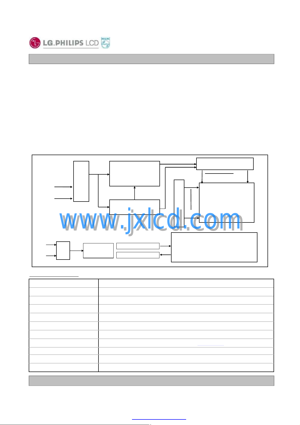
RGB, Dclk, DE
Hsync, Vsync
(LVDS 2 port)
V
(+12V)
LCD
www.jxlcd.com
+24.0V
GND
(14Pin)
(30pin)
www.jxlcd.com
CN2
General Features
CN1
Inverter
20.1 inches(511.133mm) diagonal (Aspect ratio 16:10)Active Screen Size
461.4(H) x 296.8 (V) x 36.9(D) mm (Typ.)Outline Dimension
0.258mm x 0.258mmPixel Pitch
1680 horiz. By 1050 vert. Pixels RGB strip arrangementPixel Format
Timing Control
Block
Power Circuit Block
2pin x 5CNs (High)
2pin x 1CNs (Low)
Source Driver Circuit
Gate Driver circuit
G1
TFT-LCD Panel
(1680 × 1050 pixels)
G1050
Back light Assembly
(Direct Light Type_10CCFL)
S1680S1
8bit, 16,7 M colorsColor Depth
470 cd/m2 (Center 1 point, Typ.)Luminance, White
Viewing Angle Free ( R/L 178(Typ.), U/D 178(Typ))Viewing Angle (CR>10)
Total 54.81 Watt(Typ.) (5.81 Watt@VLCD, 49 Watt@470cd)Power Consumption
2680 g (Typ.)Weight
Transmissivemode, normally blackDisplay Operating Mode
Glare treatment of the front polarizerSurface Treatment
Ver. 1.0 June .8. 2006
PDF created with pdfFactory Pro trial version www.pdffactory.com
4/ 31
LM201WE2
Liquid Crystal Display
Product Specification
2. Absolute Maximum Ratings
The following are maximum values which, if exceeded, may cause faulty operation or damage to the unit.
Table 1. ABSOLUTE MAXIMUM RATINGS
Parameter Notes
Power Input Voltage
Operating Temperature
Storage Temperature
Operating Ambient Humidity
Storage Humidity
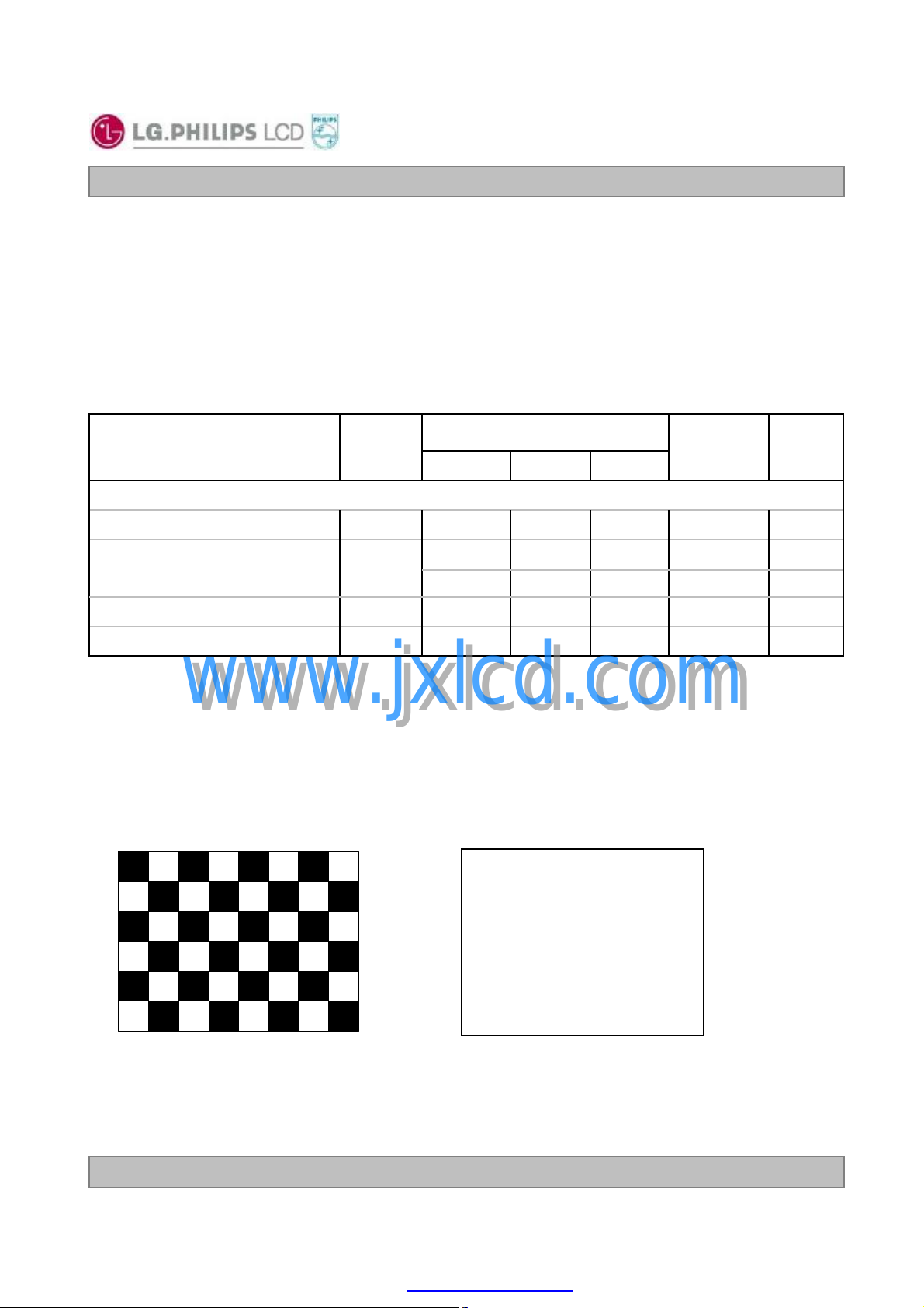
Note : 1. Temperature and relative humidity range are shown in the figure below.
Wet bulb temperature should be 39 °C Max, and no condensation of water.
www.jxlcd.com
www.jxlcd.com
Symbol
Values
MaxMin
500TOP
60-20TST
90%
60
60%
Units
Vdc14.0-0.3VLCD
°C
°C
at 25 ± 2 °C
1
1
1%RH9010HOP
1%RH9010HST
Wet Bulb
50
Temperature [C]
40
30
20
10
0
10 20 30 40 50 60 70 800-20
Dry Bulb Temperature [C]
Ver. 1.0 June .8. 2006
40%
10%
Storage
Operation
Hum idity [(%)RH]
5/ 31
PDF created with pdfFactory Pro trial version www.pdffactory.com
LM201WE2
Liquid Crystal Display
Product Specification
3. Electrical Specifications
3-1. Electrical Characteristics
It requires two power inputs. One is employed to power the LCD electronics and to drive the TFT array and
liquid crystal. The second input power for the CCFL, is typically generated by an inverter. The inverter is an
external unit to the LCDs.
Table 2_1. ELECTRICAL CHARACTERISTICS
Parameter Symbol
MODULE :
ILCDPower Supply Input Current
Note :
1. The specified current and power consumption are under the V
whereas mosaic pattern(8 x 6) is displayed and fVis the frame frequency.
2. The current is specified at the maximum current pattern.
3. The duration of rush current is about 2ms and rising time ofpower Input is 1ms(min.).
White : 255Gray
Black : 0Gray
www.jxlcd.com
www.jxlcd.com
Maximum current pattern
Values
MaxTypMin
=12.0V, 25 ± 2°C,fV=60Hz condition
LCD
NotesUnit
Vdc12.612.011.4VLCDPower Supply Input Voltage
1mA5604662mA6865721Watt6.725.59-PLCDPower Consumption
3A3--IRUSHRush current
Mosaic Pattern(8 x 6)
Ver. 1.0 June .8. 2006
PDF created with pdfFactory Pro trial version www.pdffactory.com
White Pattern
6/ 31
Product Specification
Table 2_2. INVERTERELECTRICAL CHARACTERISTICS
LM201WE2
Liquid Crystal Display
ConditionSymbolParameter
Inverter :
Input Voltage
Input Current
LAMP :
Notes :
www.jxlcd.com
1. The input voltage ripple is limited below 400mVp-p.
2.The specified current and power consumption are under the typical supply Input voltage, 24V.
3.The life is determined as the time at which luminance of the lamp is 50% compared to that of initial
value at the typical lamp current on condition of continuousoperating at 25 ± 2°C.
4. Electrical characteristics are determined after the unit has been ‘ON’ and stable for approximately
30min in a dark environment at 25 °C± 2°C.
www.jxlcd.com
DDB
DDB
Values
Max.Typ.Min.
Unit
V262422V
A2.281.92VBR= 3.3VI
Watt50.746.141.5VBR= 3.3VPBInput Power
V5.0-2.0Lamp ON = HighVON/OFFB/L on/off control
V0.8-0.0Lamp OFF =Low
V3.3-0.0VBRBrightness Adj
Notes
1
2
2
3Hrs50,000Life time
Ver. 1.0 June .8. 2006
PDF created with pdfFactory Pro trial version www.pdffactory.com
7/ 31
LM201WE2
Liquid Crystal Display
Product Specification
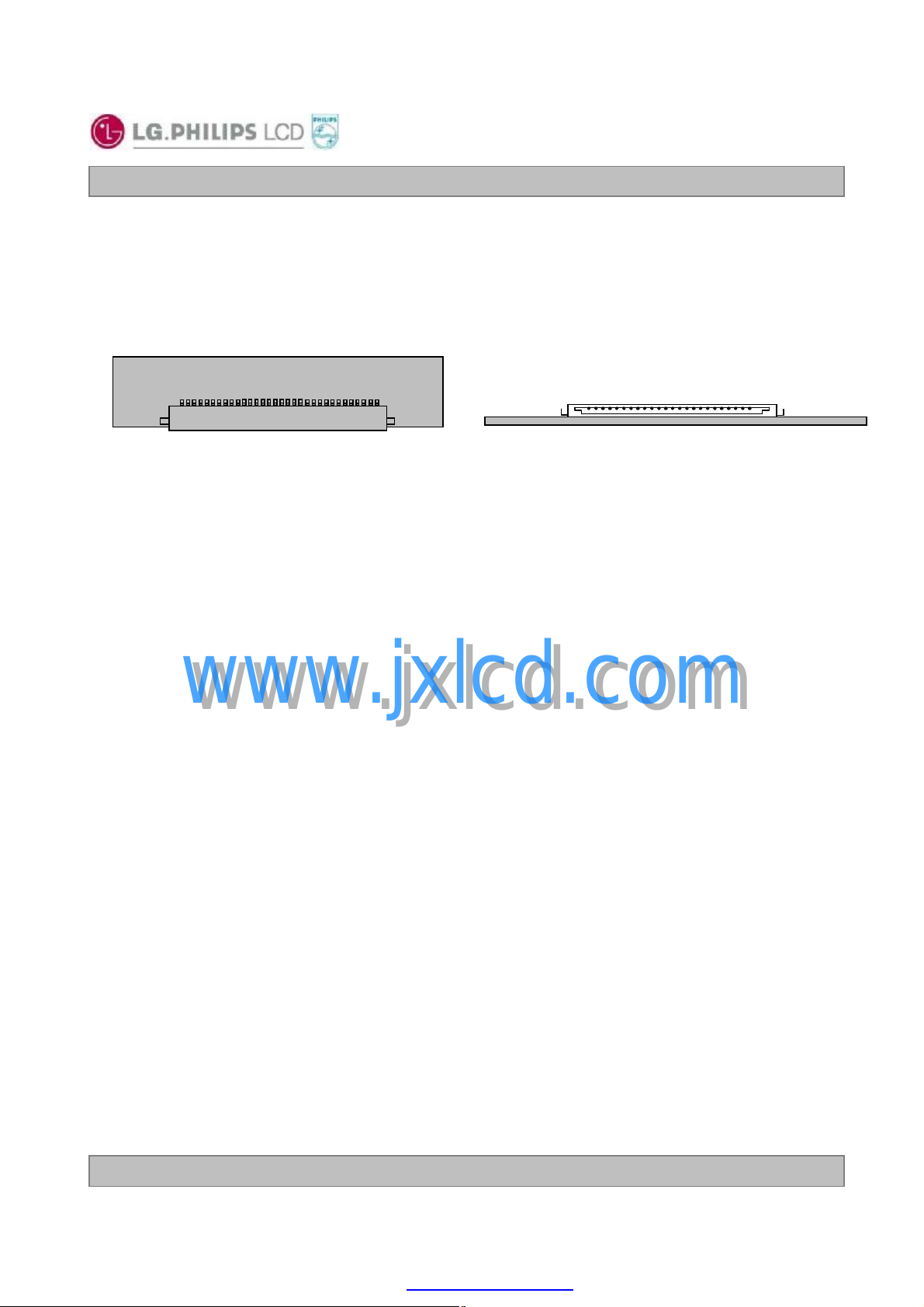
3-2. Interface Connections
This LCD employs Two interface connections, a 30 pin connector is used for the module electronics and a
14Pin Connector is used for the integral backlight system.
3-2-1. Interface Connections
-LCD Connector(CN1) : IS100-L30B-C23(Manufactured by UJU) or Equivalent
-Mating Connector : FI-XC30C2L (Manufactured by JAE) or Equivalent
Table 3. MODULE CONNECTOR(CN1) PIN CONFIGURATION
Pin No
1
2
3
4
5
6
7
8
9
10
11
12
13
14
15
16
17
18
19
20
21
22
23
24
25
26
27
28
29
30
Symbol Description
FR0M
FR0P
FR1M
FR1P
FR2M
FR2P
GND
FCLKINM
FCLKINP
FR3M
FR3P
SR0M
SR0P
www.jxlcd.com
www.jxlcd.com
GND
SR1M
SR1P
GND
SR2M
SR2P
SCLKINM
SCLKINP
SR3M
SR3P
GND
GND
DCR
DIM
VLCD
VLCD
VLCD
Minus signal of odd channel 0 (LVDS)
Plus signal of odd channel 0 (LVDS)
Minus signal of odd channel 1 (LVDS)
Plus signal of odd channel 1 (LVDS)
Minus signal of odd channel 2 (LVDS)
Plus signal of odd channel 2 (LVDS)
Ground
Minus signal of odd clock channel (LVDS)
Plus signal of odd clock channel (LVDS)
Minus signal of odd channel 3 (LVDS)
Plus signal of odd channel 3 (LVDS)
Minus signal of even channel 0 (LVDS)
Plus signal of even channel 0 (LVDS)
Ground
Minus signal of even channel 1 (LVDS)
Plus signal of even channel 1 (LVDS)
Ground
Minus signal of even channel 2 (LVDS)
Plus signal of even channel 2 (LVDS)
Minus signal of even clock channel (LVDS)
Plus signal of even clock channel (LVDS)
Minus signal of even channel 3 (LVDS)
Plus signal of even channel 3 (LVDS)
Ground
Ground
DCR-Enable ON 2.5~3.3V, OFF 0~0.8V
DIM-Out 0.5V ~ 3.3V
Power Supply +12.0V
Power Supply +12.0V
Power Supply +12.0V
First data
Second data
Note: 1. All GND(ground) pins should be connected together and to Vss which should also be connected to
the LCD’s metal frame.
2. All VLCD (power input) pins should be connected together.
3. Input Level of LVDS signal is based on the IEA 664Standard.
Ver. 1.0 June .8. 2006
PDF created with pdfFactory Pro trial version www.pdffactory.com
8/ 31
Product Specification
User Connector Diagram
LM201WE2
Liquid Crystal Display
#1
IS-100-L30B-C23 (UJU)
www.jxlcd.com
www.jxlcd.com
#30
#1 #30
Rear view of LCM
Ver. 1.0 June .8. 2006
PDF created with pdfFactory Pro trial version www.pdffactory.com
9/ 31
Liquid Crystal Display
Product Specification
Table 4. REQUIRED SIGNAL ASSIGNMENT FOR Flat Link (TI:SN75LVDS83) Transmitter
Pin # Require SignalPin Name Pin # Require SignalPin Name
1 Power Supply for TTL InputVCC 29 Ground pin for TTLGND
2 TTL Input (R7)D5 30 TTL Input (DE)D26
3 TTL Input (R5)D6 31 TTL Level clock InputTXCLKIN
4 TTL Input (G0)D7 32 Power Down InputPWR DWN
5 Ground pin for TTLGND 33 Ground pin for PLLPLL GND
6 TTL Input (G1)D8 34 Power Supply for PLLPLL VCC
7 TTL Input (G2)D9 35 Ground pin for PLLPLL GND
8 TTL Input (G6)D10 36 Ground pin for LVDSLVDS GND
9 Power Supply for TTL InputVCC 37 Positive LVDS differential data output 3TxOUT3+
10 TTL Input (G7)D11 38 Negative LVDS differential data output 3TxOUT3-
LM201WE2
11 TTL Input (G3)D12 39 Positive LVDS differential clock outputTXCLKOUT+
12 TTL Input (G4)D13 40 Negative LVDS differential clock outputTXCLKOUT-
13 Ground pin for TTLGND 41 Positive LVDS differential data output 2TXOUT2+
14 TTL Input (G5)D14 42 Negative LVDS differential data output 2TXOUT2-
15 TTL Input (B0)D15 43 Ground pin for LVDSLVDS GND
16 TTL Input (B6)D16 44 Power Supply for LVDSLVDS VCC
17 Power Supply for TTL InputVCC 45 Positive LVDS differential data output 1TXOUT1+
19 TTL Input (B1)D18
20 TTL Input (B2)D19
22 TTL Input (B3)D20
23 TTL Input (B4)D21
24 TTL Input (B5)D22
25 TTL Input (RSVD)D23
26 Power Supply for TTL InputVCC 54 TTL Input (R2)D2
www.jxlcd.com
www.jxlcd.com
46 Negative LVDS differential data output 1TXOUT1-18 TTL Input (B7)D17
47 Positive LVDS differential data output 0TXOUT0+
48 Negative LVDS differential data output 0TXOUT0-
49 Ground pin for LVDSLVDS GND21 Ground pin for TTL InputGND
50 TTL Input (R6)D27
51 TTL Input (R0)D0
52 TTL Input (R1)D1
53 Ground pin for TTLGND
55 TTL Input (R3)D327 TTL Input (HSYNC)D24
56 TTL Input (R4)D428 TTL Input (VSYNC)D25
Notes : Refer to LVDS Transmitter Data Sheet for detail descriptions.
Ver. 1.0 June .8. 2006
PDF created with pdfFactory Pro trial version www.pdffactory.com
10/ 31

Liquid Crystal Display
Product Specification
3-2-2. Backlight Interface
-Inverter Connector : S14B-PHA-SM3 Side entry type(Manufactured by JST) or Equivalent
-Mating Connector : PHR-14(Manufactured by JST) or Equivalent
Table 5. INVERTER CONNECTOR PIN CONFIGULATION
Power Supply +24.0V (Back light)VDDB1
Power Supply +24.0V (Back light)VDDB 2
Power Supply +24.0V (Back light)VDDB 3
Power Supply +24.0V (Back light)VDDB 4
Power Supply +24.0V (Back light)VDDB 5
Power Ground (Back light)GND6
Power Ground (Back light)GND7
LM201WE2
RemarksDescriptionSymbolPin No
Power Ground (Back light)GND9
Power Ground (Back light)GND10
NCOPEN11
www.jxlcd.com
www.jxlcd.com
Notes : 1. GND is connected tothe LCD’s metal frame.
Backlight On/off SignalVON/OFF12
Brightness Adjustable VoltageVBR13
NC (DON’T USE)OPEN14
Rear view of LCM
14
…
1
Note 1Power Ground (Back light)GND8
ON : 2.0V~5.0V
OFF : 0.0~0.8V
Max3.3V/Min0.0V
PCB
…
S14B-PHA-SM3
(JST : Japan SolderlessTerminal Co.,Ltd.)
Ver. 1.0 June .8. 2006
PDF created with pdfFactory Pro trial version www.pdffactory.com
11/ 31

LM201WE2
Liquid Crystal Display
Product Specification
3-3. Signal Timing Specifications
This is the signal timing required at the input of the User connector. All of the interface signal timing should be
satisfied with the following specifications for it’s proper operation.
Table 6. Timing Table
NoteUnitMaxTypMinSymbolITEM
ns8.268.408.55tCLKPeriod
DCLK
MHz121119112-Frequency
tCLK184018401816tHPPeriod
Hsync
Vsync
DE
(Data
Enable)
64.67464.67459.696fHFrequency
666tWVWidth
www.jxlcd.com
www.jxlcd.com
Horizontal Blank
-
168016801680tHVHorizontal Valid
808080tHBPHorizontal Back Porch
484824tHFPHorizontal Front Porch
160160136
105010501050tVVVertical Valid
21219tVBPVertical Back Porch
331tVFPVertical Front Porch
KHz
tCLK323232tWHWidth
tHP109010801066tVPPeriod
Hz6459.88356fVFrequency
tHP
tCLK
tHP
Notes: Hsyncperiod and Hsyncwidth-active should be even number times of tCLK. If thevalue is odd number
times of tCLK, display control signal can be asynchronous.In order tooperate this LCM a Hsync,
Vsyn, and DE(data enable) signals should be used.
1. The performance of the electro-optical characteristics may be influenced by variance of the vertical
refresh rates.
2. Vsyncand Hsyncshould be keep the above specification.
3. HsyncPeriod, HsyncWidth, and Horizontal Back Porch should be any times of of character
number(8).
4. The polarity of Hsync, Vsyncis not restricted.
Ver. 1.0 June .8. 2006
PDF created with pdfFactory Pro trial version www.pdffactory.com
303016-Vertical Blank
12/ 31

3-4. Signal Timing Waveforms
LM201WE2
Liquid Crystal Display
Product Specification
DCLK
First data
Second data
DE(Data Enable)
www.jxlcd.com
www.jxlcd.com
Hsync, Vsync, DE, Data
tCLK
0.5 VCC
Invalid data
Invalid data
Valid data
Pixel 0,0
Valid data
Pixel 1,0
0.7VCC
Pixel 2,0
Pixel 3,0
0.3VCC
Invalid data
Invalid data
tHP
HSync
DE(Data Enable)
VSync
DE(Data Enable)
Ver. 1.0 June .8. 2006
tWH
tHBP tHV
tVP
tWV
tVBP
tHFP
tVV tVFP
13/ 31
PDF created with pdfFactory Pro trial version www.pdffactory.com

LM201WE2
Liquid Crystal Display
Product Specification
3-5. Color Data Reference
The Brightness of each primary color(red,green,blue) is based onthe 8-bit gray scale data input for the color;
the higher the binary input, the brighter the color. The table below provides a reference for color versus data
input.
Table 7. COLOR DATA REFERENCE
Input Color Data
Basic
Color
RED
Color
Black 0 0 0 0 0 0 0 00 0 0 0 0 0 0 00 0 0 0 0 0 0 0
Red (255)
Green (255)
Blue (255)
Cyan
Magenta
Yellow
White
www.jxlcd.com
www.jxlcd.com
MSB LSB
RED
MSB LSB
GREEN
MSB LSB
B7 B6 B5 B4 B3 B2 B1 B0G7 G6 G5 G4 G3 G2 G1 G0R7 R6 R5 R4 R3 R2 R1 R0
0 0 0 0 0 0 0 00 0 0 0 0 0 0 01 1 1 1 1 1 1 1
0 0 0 0 0 0 0 01 1 1 1 1 1 1 10 0 0 0 0 0 0 0
1 1 1 1 1 1 1 10 0 0 0 0 0 0 00 0 0 0 0 0 0 0
1 1 1 1 1 1 1 11 1 1 1 1 1 1 10 0 0 0 0 0 0 0
1 1 1 1 1 1 1 10 0 0 0 0 0 0 01 1 1 1 1 1 1 1
0 0 0 0 0 0 0 01 1 1 1 1 1 1 11 1 1 1 1 1 1 1
1 1 1 1 1 1 1 11 1 1 1 1 1 1 11 1 1 1 1 1 1 1
0 0 0 0 0 0 0 00 0 0 0 0 0 0 00 0 0 0 0 0 0 0RED (000) Dark
0 0 0 0 0 0 0 00 0 0 0 0 0 0 00 0 0 0 0 0 0 1RED (001)
0 0 0 0 0 0 0 00 0 0 0 0 0 0 01 1 1 1 1 1 1 0RED (254)
0 0 0 0 0 0 0 00 0 0 0 0 0 0 01 1 1 1 1 1 1 1RED (255)
0 0 0 0 0 0 0 00 0 0 0 0 0 0 00 0 0 0 0 0 0 0GREEN (000) Dark
BLUE
............
GREEN
BLUE (000) Dark
BLUE
Ver. 1.0 June .8. 2006
PDF created with pdfFactory Pro trial version www.pdffactory.com
0 0 0 0 0 0 0 00 0 0 0 0 0 0 10 0 0 0 0 0 0 0GREEN (001)
............
0 0 0 0 0 0 0 01 1 1 1 1 1 1 00 0 0 0 0 0 0 0GREEN (254)
0 0 0 0 0 0 0 01 1 1 1 1 1 1 10 0 0 0 0 0 0 0GREEN (255)
0 0 0 0 0 0 0 00 0 0 0 0 0 0 00 0 0 0 0 0 0 0
0 0 0 0 0 0 0 10 0 0 0 0 0 0 00 0 0 0 0 0 0 0BLUE (001)
............
1 1 1 1 1 1 1 00 0 0 0 0 0 0 00 0 0 0 0 0 0 0BLUE (254)
1 1 1 1 1 1 1 10 0 0 0 0 0 0 00 0 0 0 0 0 0 0BLUE (255)
14/ 31

3-6. Power Sequence
LM201WE2
Liquid Crystal Display
Product Specification
Power Supply, VLCD
Interface Signal, Vi
(Digital RGB signal,
SCDT ,Vsync, Hsync,
DE, Clock to LVDS
Transmitter)
Power Supply for
Backlight Inverter
www.jxlcd.com
Table 8. POWER SEQUENCE
www.jxlcd.com
Parameter
VLCD
10%
0V
0V
90% 90%
T2 T5 T6 T7
T1
10%
LAMP OFF
Valid data
T3
LAMP ON
Values
10%
T4
MaxTypMin
--200T4
10%
LAMP OFF
Units
ms10--T1
ms50-0.01T2
ms--200T3
ms
ms50-0.01T5
ms10-0.01T6
s--1T7
Notes :1. Please avoid floating state of interface signal at invalid period.
2. When the interface signal is invalid, be sure to pull down the power supply for LCD V
3. Lamp power must be turn on after power supply for LCD an interface signal are valid.
Ver. 1.0 June .8. 2006
PDF created with pdfFactory Pro trial version www.pdffactory.com
LCD
to 0V.
15/ 31

3-6-2 Power Sequence for Inverter
V
BL
Power Supply_V
BL
10%
0V
90%
T1
LM201WE2
Liquid Crystal Display
Product Specification
Lamp ON/OFF
Lamp Dimmer
www.jxlcd.com
www.jxlcd.com
Vin Dipping
Vin_typ
0V
LAMP OFF
T2
T4
LAMP ON
T3
T5
Vin_dip≤ Vin_typ × 0.2
Table 8_2. Power Sequence
Parameter
T1
T2
T3
T4
T5
Ver. 1.0 June .8. 2006
Min.
1
200
-
500
-
Values
Typ.
-
-
-
PDF created with pdfFactory Pro trial version www.pdffactory.com
Max.
30
-
50
--
10-
Units
ms
ms
ms
ms
ms
Notes
16/ 31

LM201WE2
Liquid Crystal Display
Product Specification
4. Optical Specification
Optical characteristics are determined after the unit has been ‘ON’ and stable for approximately 30 minutes in
a dark environment at 25±2°C. The values specified are at an approximate distance 50cm fromthe LCD
surface at a viewing angle of Φ and θ equal to 0 °.
FIG. 1 presents additional information concerning the measurement equipment and method.
Optical Stage(x,y)
LCD Module
FIG. 1 Optical Characteristic Measurement Equipment and Method
Table 9. OPTICAL CHARACTERISTICS
SymbolParameter
Contrast Ratio
Surface Luminance, 1pts
Luminance Variation
www.jxlcd.com
Response Time
Color Coordinates
[CIE1931]
Horizontal
Vertical
Viewing Angle (CR>10)
General
Effective
Ver. 1.0 June .8. 2006
Horizontal
Vertical
Horizontal
Vertical 178
Rise Time
www.jxlcd.com
Decay Time
Gray To Gray
RED
GREEN
BLUE
WHITE
WH
WHITE
R
D
GTG_AVR
GTG_MAX
Rx
θ
CST_H
θ
CST_V
θ
H
θ
V
θ
GMA_H
θ
GMA_V
50cm
Ta=25 °C, V
Typ
-0.03
=12.0V, fV=60Hz Dclk=119MHz, IBL=5.5mA
LCD
Values
MaxTypMin
0.640
0.340Ry
0.290Gx
0.615Gy
0.145Bx
0.070By
0.313Wx
0.329Wy
+0.03
Pritchard 880 or
equivalent
-700450CR
-16001000CR(With DCR)
-470400L
Typ
-178-
-178170
-178170
-178-
Units
cd/m
%72Color gamut
degree-178-
Notes
1
2
2
31.45--δ
4ms105-Tr
4ms247-Tr
5ms-6-T
5ms-10-T
6Color shift
7degree
8degree
92.2Gray Scale
17/ 31
PDF created with pdfFactory Pro trial version www.pdffactory.com

Product Specification
…
Notes 1. Contrast Ratio(CR) is defined mathematically as :
LM201WE2
Liquid Crystal Display
Contrast Ratio =
2. Surface luminance is luminance value at No.1 pointacross the LCD surface 50cm
from the surface with all pixels displaying white. For more information see FIG 2.
3. The variation in surface luminance , δ WHITE is defined as :
δ
WHITE
Measuring point for surface luminance & measuring point for luminance variation
www.jxlcd.com
www.jxlcd.com
B
Surface Luminance with all white pixels
Surface Luminance with all black pixels
)L .. ,L,Minimum(L
=
A
2 3
on9on2on1
)L .... ,L ,(L Maximum
on9on2on1
H
(%)100
×
4
H/10
V
V/10
A : H/4 mm
B : V/4 mm
@ H,V : Active Area
Ver. 1.0 June .8. 2006
5
7 8
FIG. 2 Measure Point for Luminance
1
6
9
Active Area
18/ 31
PDF created with pdfFactory Pro trial version www.pdffactory.com

Liquid Crystal Display
Product Specification
4. The response time is defined as the following figure and shall be measured by switching
the input signal for “black” and “white”.
Response time is the time required for the display to transitionfrom black to white (Rise Time,
TrR) and from white to black (Decay Time, TrD).
-Measure Condition : DCR Off
100
Optical
Response
90
10
TrR
0
black
FIG. 3 Response Time
white
TrD
black
LM201WE2
5. The Gray to Gray response time is defined as the following figure and shall be measured
by switching the input signal for “Gray To Gray “.
-Measure Condition : DCR Off
-Gray step : 5 Step
www.jxlcd.com
www.jxlcd.com
-T
GTG_AVR
-T
GTG_MAX
is the total average time at rising time and falling time for “Gray To Gray “.
is the max time at rising time or falling time for “Gray To Gray “.
Rising Time
Gray to Gray
G0G63G127G191G255
G255Falling Time
G191
G127
G63
G0
Ver. 1.0 June .8. 2006
PDF created with pdfFactory Pro trial version www.pdffactory.com
19/ 31

Product Specification
6. Color shift is the angle at which the color difference is lower than 0.04.
-Color difference(Δu’v’)
LM201WE2
Liquid Crystal Display
xl
u’=
Δu’v’ = (u’1-u’2)2+(v’1-v’2)
-Pattern size : 25% Box size
-Viewing angle direction of color shift : Horizontal, Vertical
φ = 90。
(12:00)
φ = 180。
(9:00)
www.jxlcd.com
www.jxlcd.com
TFT LCD
MODULE
4x
-2x + 12y + 3
θ = 0。
yu
z
z' yd
θ
2
A
φ = 270。
(6:00)
v’=
u’1, v’1 : u’v’ value at viewing angle direction
u’2, v’2 : u’v’ value at front (θ=0)
φ
9y
-2x + 12y +3
φ = 0。
(3:00) xr
25% Box size
Viewing angle direction
Average RGB values in Bruce RGB for Macbeth Chart
Ver. 1.0 June .8. 2006
Bluish greenBlue flowerFoliageBlue skyLight skinDark skin
114129778520698R
19911810211214256G
1781854616112345B
Orange yellowYellow greenPurpleModerate redPurplish blueOrange
2301607621156219R
162193396769104G
2958868717424B
cyanMagentaYellowRedGreenBlue
352072411977226R
126622122714832G
172151363765145B
blackNeutral 3.5Neutral 5Neutral 6.5Neutral 8White
2263110155206240R
2263110155206240G
2263110155206240B
20/ 31
PDF created with pdfFactory Pro trial version www.pdffactory.com

LM201WE2
Liquid Crystal Display
Product Specification
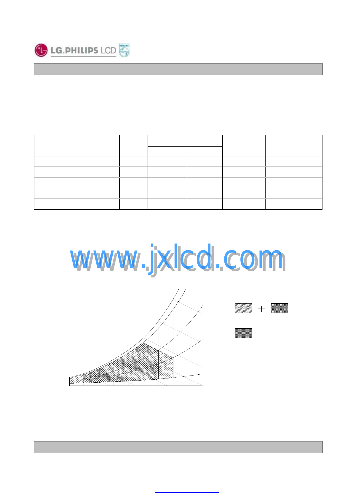
7. Viewing angle(general) is the angle at which the contrast ratio is greater than 10.
8. Effective viewing angle is the angle at which the gamma shift of gray scale is lower than 0.3.
r
LaVL +=
b
Here the Parameter α and γ relate the signal level V to the luminance L.
The GAMMA we calculate from the log-log representation (Fig. 2)
9. Gray scale specification
Gamma Value is approximately 2.2. For more information see Table 10.
-Measure Condition : DCR Off
www.jxlcd.com
www.jxlcd.com
Table 10. Gray Scale Specification
31
63
95
127
b
Relative Luminance [%] (Typ.)Gray Level
0.30
1.1
4.57
11.3
21.4
+=−
)log()log()log( aVrLL
159
191
223
255
Ver. 1.0 June .8. 2006
PDF created with pdfFactory Pro trial version www.pdffactory.com
35.2
52.8
74.4
100
21/ 31

LM201WE2
Liquid Crystal Display
Product Specification
5. Mechanical Characteristics
The contents provide general mechanical characteristics. In addition the figures in the next page are detailed
mechanical drawing of the LCD.
461.4mmHorizontal
Outline Dimension
Bezel Area
Active Display Area
2680g (Typ.), 2810g (Max.)Weight
Glare treatment of the front polarizerSurface Treatment
Notes : Please refer to a mechanic drawing in terms of toleranceat the next page.
www.jxlcd.com
www.jxlcd.com
296.8mmVertical
36.9mmDepth
438.4mmHorizontal
275.9mmVertical
433.44mmHorizontal
270.90mmVertical
Ver. 1.0 June .8. 2006
PDF created with pdfFactory Pro trial version www.pdffactory.com
22/ 31

<FRONT VIEW><FRONT VIEW>
LM201WE2
Liquid Crystal Display
Product Specification
www.jxlcd.com
www.jxlcd.com
Ver. 1.0 June .8. 2006
PDF created with pdfFactory Pro trial version www.pdffactory.com
23/ 31

<REAR VIEW>
LM201WE2
Liquid Crystal Display
Product Specification
www.jxlcd.com
www.jxlcd.com
LM201WE2
(SL)(A1)
Before Improvement : F11
After Improvement : F12
201574K100001 F12
Ver. 1.0 June .8. 2006
PDF created with pdfFactory Pro trial version www.pdffactory.com
24/ 31

Product Specification
6. Reliability
Environment test condition
No Test Item Conditions
1 High temperature storage test Ta= 60°C 240hr
2 Low temperature storage test Ta= -20°C 240hr
3 High temperature operation test Ta= 50°C 60%RH 240hr
4 Low temperature operation test Ta= 0°C 240hr
5 Humidity condition operation 10%RH ~ 90%RH
6 Humidity condition storage 10%RH ~ 90%RH
1.Sinusoidal Vibration
1.0 G zero to peak.
10 to 500 Hz, 0.5 oct/ min sweep rate.
Vibration test
7
(non-operating)
www.jxlcd.com
www.jxlcd.com
10 to 500, 10 Hz, one sweep along each axis.
2.Random Vibration
0.002 G2/Hz, 10 to 500 Hz, nominal 1 GRMS.
One hour for each of the three axes.
or 5-200Hz:14.406m /s2rms 33min for each of the three axes..
LM201WE2
Liquid Crystal Display
8
9
10
{ Result Evaluation Criteria }
There should be no change which might affect the practical display function when the display quality
test is conducted under normal operating condition.
Notes : Please refer to page 5 an Environment test condition
Ver. 1.0 June .8. 2006
Shock test
(non-operating)
Altitude
storage / shipment
operation
ESD test
(Non-operation)
Shock level : 100G
Waveform: half sine wave, 2ms
Direction : ±X, ±Y, ±Z
One time each direction
0 - 40,000 feet (12,192m)
0 - 12,000 feet (3,048m)
Condition : 150pF, 330Ω
Terminal : 200V
Chassis : 10KV
25/ 31
PDF created with pdfFactory Pro trial version www.pdffactory.com

LM201WE2
Liquid Crystal Display
Product Specification
7. International Standards
7-1. Safety
a) UL 60950-1:2003, First Edition, Underwriters Laboratories, Inc.,
Standard for Safety of Information Technology Equipment.
b) CAN/CSA C22.2, No. 60950-1-03 1stEd. April 1, 2003, Canadian Standards Association,
Standard for Safety of Information Technology Equipment.
c) EN 60950-1:2001, First Edition,
European Committee for ElectrotechnicalStandardization(CENELEC)
European Standard for Safety of Information Technology Equipment.
7-2. EMC
a) ANSI C63.4 “Methods of Measurement of Radio-Noise Emissions from Low-Voltage Electrical and
Electrical Equipment in the Range of 9kHZ to 40GHz. “American National Standards Institute(ANSI),
1992
b) C.I.S.P.R. “Limits and Methods of Measurement of Radio Interface Characteristics of Information
Technology Equipment.“ International Special Committee on Radio Interference.
c) EN 55022 “Limits and Methods of Measurement of Radio Interface Characteristics of Information
Technology Equipment.“ European Committee for ElectrotechnicalStandardization.(CENELEC), 1998
( Including A1: 2000 )
www.jxlcd.com
www.jxlcd.com
Notes : The LM201WE2-SLA1 is applied ROHS items
Ver. 1.0 June .8. 2006
26/ 31
PDF created with pdfFactory Pro trial version www.pdffactory.com

Product Specification
8. Packing
8-1. Designation of Lot Mark
a) Lot Mark
A B C D E F G H I J K L M
A,B,C : SIZE(INCH) D : YEAR
E : MONTH F : FACTORY CODE
G : ASSEMBLY CODE H ~ M : SERIAL NO.
Note
1. YEAR
LM201WE2
Liquid Crystal Display
Year
Mark
2. MONTH
Month
Mark
www.jxlcd.com
3. FACTORY CODE
Factory Code
4. SERIAL NO.
b) Location of Lot Mark
Serial No. is printed on the label. The label is attached to thebackside of the LCD module.
This is subject to change without prior notice.
www.jxlcd.com
LPL Gumi
Mark
Mark 100001~199999, 200001~299999, 300001~399999, …., A00001~A99999, ….., Z00001~Z99999
K
200320022001
200452005
321
4
Apr5May
4
LPL Nanjing
C
2006720078200892009
6
Jun7Jul8Aug9Sep
6
HEESUNG
D
2010
0
Oct
A
Nov
B
DecMarFebJan
C321
Ver. 1.0 June .8. 2006
PDF created with pdfFactory Pro trial version www.pdffactory.com
27/ 31

8-2. Packing Form
a) Package quantity in one box : 6EA
b) Box Size : 409 X 489 X 543
LM201WE2
Liquid Crystal Display
Product Specification
www.jxlcd.com
www.jxlcd.com
Ver. 1.0 June .8. 2006
PDF created with pdfFactory Pro trial version www.pdffactory.com
28/ 31

8-3. Pallet Form
LM201WE2
Liquid Crystal Display
Product Specification
www.jxlcd.com
www.jxlcd.com
Ver. 1.0 June .8. 2006
PDF created with pdfFactory Pro trial version www.pdffactory.com
29/ 31

LM201WE2
Liquid Crystal Display
Product Specification
9. PRECAUTIONS
Please pay attention to the followings when you use this TFT LCDmodule.
9-1. MOUNTING PRECAUTIONS
(1) You must mount a module using holes arranged in four cornersor four sides.
(2) You should consider the mounting structure so that uneven force (ex. Twisted stress) is not applied to the
module. And the case on which a module is mounted should have sufficient strength so that external
force is not transmitted directly to the module.
(3) Please attach the surface transparent protective plate to the surface in order to protect the polarizer.
Transparent protective plate should have sufficient strength in order to the resist external force.
(4) You should adopt radiation structure to satisfy the temperature specification.
(5) Acetic acid type and chlorine type materials for the cover case are not desirable because the former
generates corrosive gas of attacking the polarizer at high temperature and the latter causes circuit break
by electro-chemical reaction.
(6) Do not touch, push or rub the exposed polarizerswith glass, tweezers or anything harder than HB
pencil lead. And please do not rub with dust clothes with chemical treatment.
Do not touch the surface of polarizer for bare hand or greasy cloth.(Some cosmetics are detrimental
to the polarizer.)
(7) When the surface becomes dusty, please wipe gently with absorbent cotton or other soft materials like
chamois soaks with petroleum benzene. Normal-hexane is recommended for cleaning the adhesives
used to attach front / rear polarizers. Do not use acetone, toluene and alcohol because they cause
chemical damage to the polarizer.
(8) Wipe off saliva or water drops as soon as possible. Their long time contact with polarizer causes
deformations and color fading.
(9) Do not open the case because inside circuits do not have sufficient strength.
www.jxlcd.com
www.jxlcd.com
9-2. OPERATING PRECAUTIONS
(1) The spike noise causes the mis-operation of circuits. It should be lower than following voltage:
V=±200mV(Over and under shoot voltage)
(2) Response time depends on the temperature.(In lower temperature, it becomes longer.)
(3) Brightness depends on the temperature. (In lower temperature, it becomes lower.)
And in lower temperature, response time(required time that brightness is stable after turned on) becomes
longer.
(4) Be careful for condensation at sudden temperature change. Condensation makes damage to polarizer or
electrical contacted parts. And after fading condensation, smearor spot will occur.
(5) When fixed patterns are displayed for a long time, remnant image is likely to occur.
(6) Module has high frequency circuits. Sufficient suppression to the electromagnetic interference shall be
done by system manufacturers. Grounding and shielding methods may be important to minimized the
interference.
(7) Please do not give any mechanical and/or acoustical impact to LCM. Otherwise, LCM can not be
operated its full characteristics perfectly.
(8) A screw which is fastened up the steels should be a machine screw (if not, it causes metallic foreign
material and deal LCM a fatal blow)
(9)Please do not set LCD on its edge.
Ver. 1.0 June .8. 2006
30/ 31
PDF created with pdfFactory Pro trial version www.pdffactory.com

LM201WE2
Liquid Crystal Display
Product Specification
9-3. ELECTROSTATIC DISCHARGE CONTROL
Since a module is composed of electronic circuits, it is not strong to electrostatic discharge. Make certain that
treatment persons are connected to ground through wrist band etc. And don’t touch interface pin directly.
9-4. PRECAUTIONS FOR STRONG LIGHT EXPOSURE
Strong light exposure causes degradation of polarizer and color filter.
9-5. STORAGE
When storing modules as spares for a long time, the following precautions are necessary.
(1) Store them in a dark place. Do not expose the module to sunlight or fluorescent light. Keep the
temperature between 5°C and 35°C at normal humidity.
(2) The polarizer surface should not come in contact with any other object.
It is recommended that they be stored in the container in which they were shipped.
9-6. HANDLING PRECAUTIONS FOR PROTECTION FILM
(1) The protection film is attached to the bezel with a small masking tape.
When the protection film is peeled off, static electricityis generated between the film and polarizer.
This should be peeled off slowly and carefully by people who are electrically grounded and with well
ion-blown equipment or in such a condition, etc.
(2) When the module with protection film attached is stored for a long time, sometimes there remains a
very small amount of glue still on the bezel after the protection film is peeled off.
(3) You can remove the glue easily. When the glue remains on thebezel surface or its vestige is
recognized, please wipe them off with absorbent cotton waste or other soft material like chamois
soaked with normal-hexane.
www.jxlcd.com
www.jxlcd.com
Ver. 1.0 June .8. 2006
PDF created with pdfFactory Pro trial version www.pdffactory.com
31/ 31
 Loading...