

LG LG-K130F Schematic
MOBILE PHONE
SERVICE MANUAL
CAUTION
BEFORE SERVICING THE UNIT, READ THE “SAFETY PRECAUTIONS” IN THIS MANUAL
MODEL : LG-K130F
Internal Use Only
Date: June 2016 / Issue 1.0
1
1. INTRODUCTION................................................. 3
2
1.1 Purpose
1.2 Regulatory Information
2. PERFORMANCE................................................... 4
2.1 Band Specification
2.2 HW Features
2.3 RSSI Display
2.4 Current consumption
2.5 Battery bar
2.6 SW Specification
3. TROUBLE SHOOTING..........................................10
3.1 Checking XO Block
3.2 Transceiver DC Power Supply
3.3 DC-DC Block
3.4 ASM Block
3.5 GSM RF Part
3.6 WCDMA RF Part
3.7 LTE RF Part
3.8 Power
3.9 Charger
3.10 Audio
3.11 LCD
3.12 Touch
3.13 Sensor
3.14 USB
3.15 CAMERA
3.16 Connectivity Part
Table Of Contents
6. BGA PIN MAP............................................................ 121
7. PCB LAYOUT…........................................................... 122
8. HIDDEN MENU.......................................................... 131
9. DOWNLOAD….......................................................... 134
10. CALIBRATION......................................................... 135
11. DISASSEMBLE GUIDE............................................ 136
12. EXPLODED VIEW………………………………………... 144
13. REPLACEMENT PART LIST..…………………………. 145
4. BLOCK DIAGRAM…........................................... 96
5. CIRCUIT DIAGRAM............................................ 103
LGE Internal Use Only
Copyright ⓒ 2016 LG Electronics. Inc. All right
reserved. Only training and service purposes
1. INTRODUCTION
3
1.1 Purpose
This manual provides the information necessary to repair, calibration, description and download the features of this model.
1.2 Regulatory Information
A. Security
This material is prohibited to share and release to unauthorized person, in accordance with the regulations, LG Electronics, Civil / criminal
responsibility in accordance with the relevant provisions violate.
B. Precautions for repair
• In case of Disassembly or As
• When using Magnetic tool for the Phone's SVC repair, you should check affect the Electric parts according to effect of Ma
• When fastening the screw, be careful not to damage the head of screw and even product.
C.
Attention
Boards, which contain Electrostatic Sensitive Device (ESD), are indicated by the sign.
Following information is ESD handling:
• Service personal should ground themselves by using a wrist, strap when exchange system board.
• When repair are made to a system board, they should spread the floor with anti-st
• Use a suitable, grounded soldering iron.
• Keep sensitive parts in these protective packages until these are used.
• When returning system board or parts like EEPROM to the Factory, use the protective package as described.
LGE Internal Use Only
sembly to repair product, be careful of a product failure caused by RF signals and Static electricity.
gnet.
atic mat which is also grounded.
Copyright ⓒ 2016 LG Electronics. Inc. All right
reserved. Only training and service purposes
2. PERFORMANCE
4
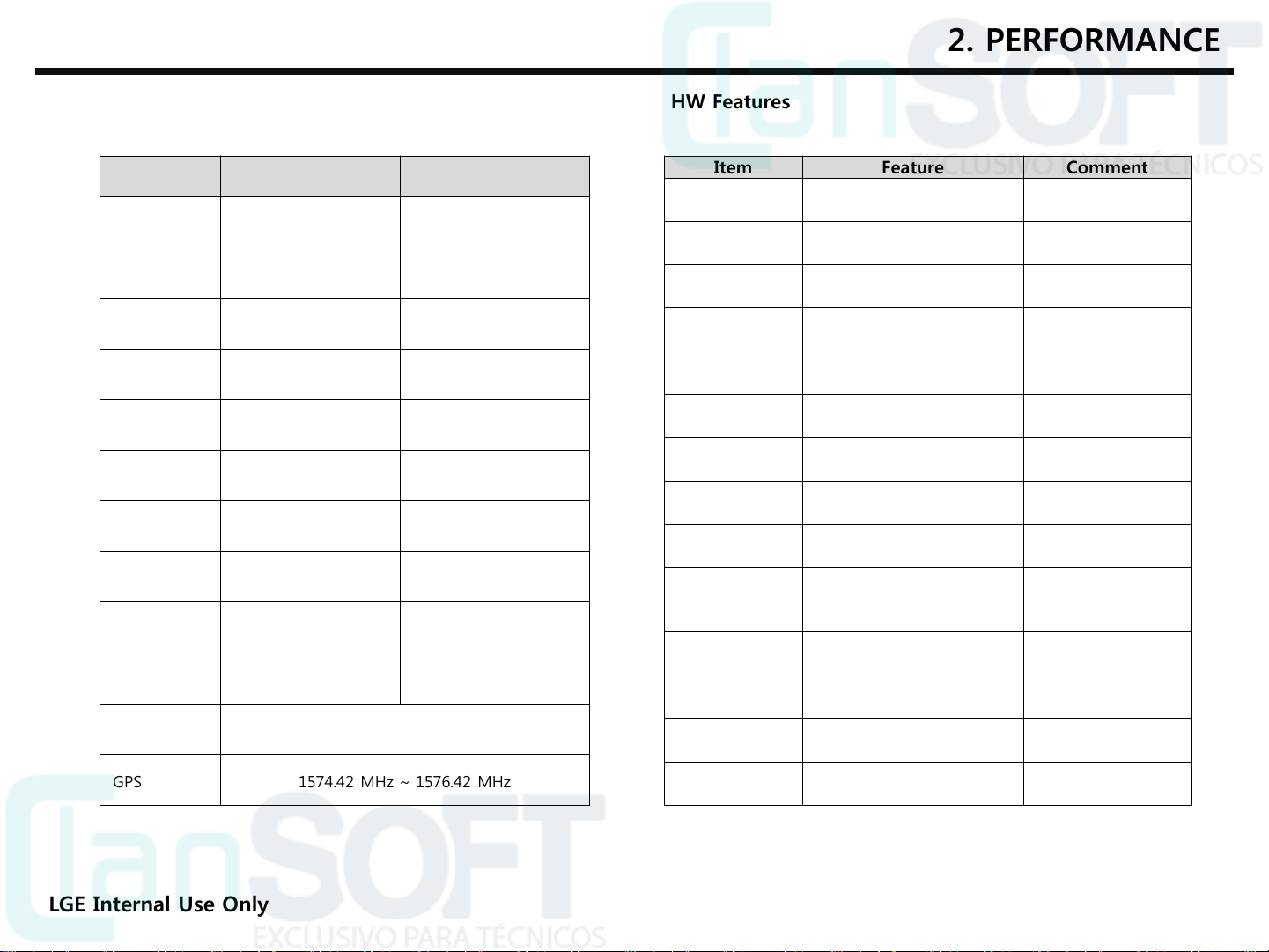
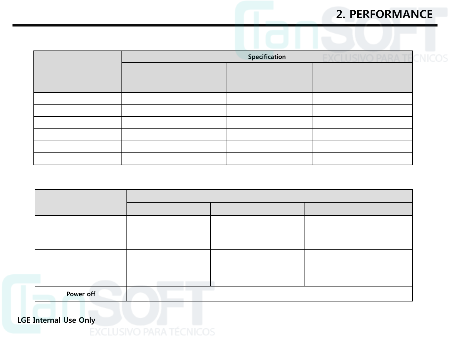
2.1 Band Specification
Support Band TX Freq (MHz) RX Freq (MHz)
GSM850 824 – 849 869 – 894
GSM900 880 – 915 925 – 960
DCS1800 1710 – 1785 1805 – 1880
PCS1900 1850 – 1910 1930 – 1990
W2100(B1) 1920 – 1980 2110 – 2170
W850(B5) 824 – 849 869 – 894
W900(B8) 880 – 915 925 – 960
LTE B3 1710 – 1785 1805 – 1880
LTE B7 2500 – 2570 2620 – 2690
LTE B28B 718 – 748 773 – 803
2.2 HW Features
Item Feature Comment
Phone type
Size
Weight
Android OS
MTK Chipset
Memory
Display
Camera
Micro SD
Audio
Bluetooth
WLAN
Touch
131.9 x 66.7 x 8.9mm
120g
L-OS
MT6735M
8GB eMMC/
1GB LPDDR3
4.5” FWVGA (854x480)
5MP AF / 2MP VT
Up to 32GB
Receiver 1106
Speaker 1511(MLD)
# of MIC. : 2
4.1 + BLE
802.11 b/g/n
With Battery
BT/WiFi Bluetooth 4.0 + BLE / 802.11 b/g/n
GPS 1574.42 MHz ~ 1576.42 MHz
LGE Internal Use Only
LTE
GPS
B3,B7,B28b
A-GPS
Copyright ⓒ 2016 LG Electronics. Inc. All right
reserved. Only training and service purposes
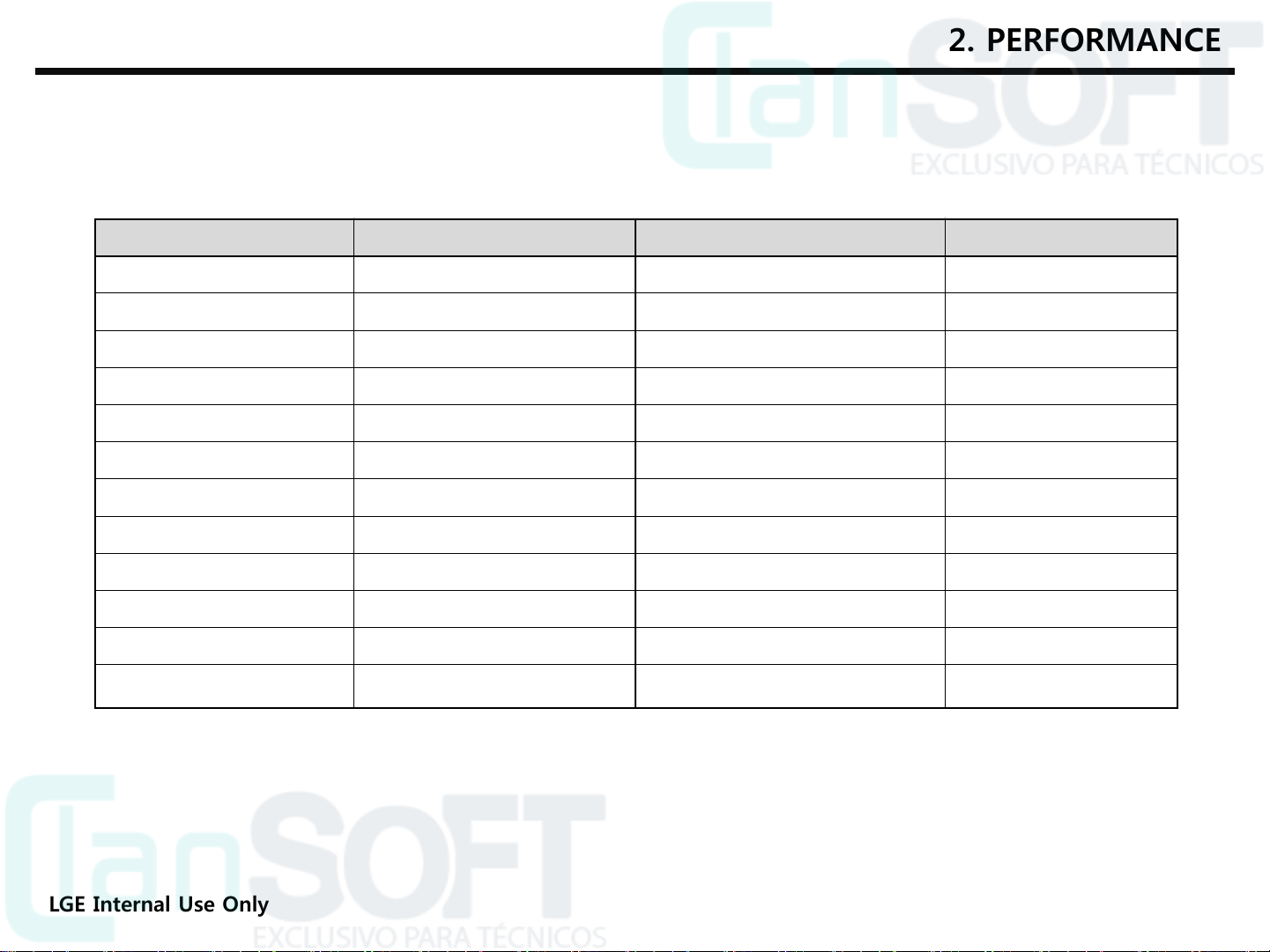
2.3 RSSI Display
5
2. PERFORMANCE
Specification
Antenna BAR
54
43
32
21
10
0 No SVC
2.4 Current consumption
Stand by current
(Sleep & Idle Avg.)
LTE (RSRP)
(B3/B7/B20B)
-85 ± 3
-95 ± 3
-105 ± 3
-115 ± 3
-128 ± 3
-131 ↓
GSM WCDMA LTE
` BT off : 7 mA
(PP = 5)
` BT on : 10 mA
(PP = 5)
WCDMA (RSCP)
(B1/B5/B8)
- 86dBm± 3dB - 91dBm± 3dB
- 91dBm± 3dB - 96dBm± 3dB
- 97dBm± 3dB - 99dBm± 3dB
- 101dBm± 3dB - 103dBm± 3dB
- 107dBm± 3dB - 105dBm± 3dB
-115 ↓ -110 ↓
Specification
` BT off : 7 mA
(DRX = 7)
` BT on : 110 mA
(DRX = 7)
GSM (RSSI)
(850/EGSM/DCS
/PCS)
` BT off : 9 mA
(DRX = 2.56sec)
` BT on : 12 mA
(DRX = 2.56sec)
LGE Internal Use Only
Talk current
Power off 500uA
300 mA
(TX Level = Max)
260 mA
(TX = 10dBm)
400 mA
(Tx= 10dBm)
Copyright ⓒ 2016 LG Electronics. Inc. All right
reserved. Only training and service purposes
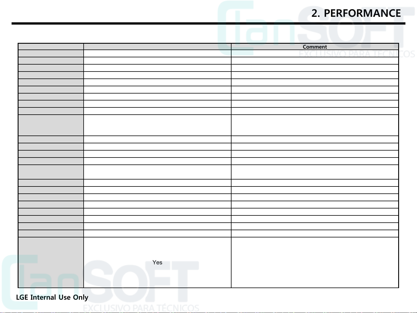
2.5 Battery bar
6
Battery Bar Specification Battery Bar Specification
Bar 20(Full) Over 98% Bar 9 -> Bar 8 43% -> 42%
Bar 20 -> Bar 19 98% -> 97% Bar 8 -> Bar 7 38% -> 37%
Bar 19 -> Bar 18 93% -> 92% Bar 7 -> Bar 6 33% -> 32%
Bar 18 -> Bar 17 88% -> 87% Bar 6 -> Bar 5 28% -> 27%
Bar 17 -> Bar 16 83% -> 82% Bar 5 -> Bar 4 23% -> 22%
Bar 16 -> Bar 15 78% -> 77% Bar 4 -> Bar 3 16% -> 15%
Bar 15 -> Bar 14 73% -> 72% Bar 3 -> Bar 2 13% -> 12%
Bar 14 -> Bar 13 68% -> 67% Bar 2 -> Bar 1 8% -> 7%
2. PERFORMANCE
※Cut Off Voltage : 3.4 ± 0.1 V
LGE Internal Use Only
Bar 13 -> Bar 12 63% -> 62% Bar 1 -> Bar 0 3% -> 2%
Bar 12 -> Bar 11 58% -> 57% Power off 2% ->1%
Bar 11 -> Bar 10 53% -> 52% Low battery pop-up 15% , 5%
Bar 10 -> Bar 9 48% -> 47%
Copyright ⓒ 2016 LG Electronics. Inc. All right
reserved. Only training and service purposes
2.6 SW Specification
Notification Sound, Phonetic name, Organization, IM,
7
Item Feature Comment
RSSI
Battery Charging
Key Volume
Audio Volume
Time / Date Display
Multi-Language
PC Sync
Speed Dial
CLIP / CLIR
Name, Phone, Email, Groups, Postal address, Ringtone,
Phone Book
Notes, Nickname, Website, Event
Last Dial Number
Last Received Number
Last Missed Number
Search by Number/Name
Group
Fixed Dial Number
Voice Memo
Network Selection
Mute
Call Divert
Call Barring
Call Duration
SMS Over GPRS
MMS MPEG4
Send / Receive / Save
0 ~ 5 Levels
0 ~ 20 Levels
0 ~ 7 Level
0 ~ 7 Level
Automatic
2. PERFORMANCE
Yes
Yes depending on build language
Yes
Yes
Yes
There is no limitation on the number of items.
It depends on available memory amount.
Yes
Yes
Yes
Yes
Yes
Yes
Yes Support voice recorder
Yes
Yes
Yes
Yes
Yes
Yes
There is no limitation on the number of items.
It depends on available memory amount.
ØSend / Receive : Yes
ØSave : depends on content type/
Support video content type list
1.video/mp4
2.video/h263
3.video/3gpp2
LGE Internal Use Only
Copyright ⓒ 2016 LG Electronics. Inc. All right
reserved. Only training and service purposes
2.6 SW Specification
8
Item Feature Comment
Voice Memo Yes Support voice recorder
Network Selection Automatic
Mute Yes
Call Divert Yes
Call Barring Yes
Call Charge (AoC) No
Call Duration Yes
SMS (EMS) There is no limitation on the number of items
SMS Over GPRS Ye s
EMS Melody / Picture
Send / Receive / Save
2. PERFORMANCE
EMS does not support.
.
It depends on available memory amount.
No
MMS MPEG4
Send / Receive / Save
Long Message MAX 2000 characters The standard of Open vender
Cell Broadcast Yes
Download Over the Web
Calendar Yes
World Clock Yes
LGE Internal Use Only
Yes Send / Receive : Ye s
Save : depends on content type
Support video content type list
1. video/mp4
2. video/h263
3. video/3gpp2
video/3gpp
Memo Yes There is no limitation on the number of items.
It depends on available memory amount.
Copyright ⓒ 2016 LG Electronics. Inc. All right
reserved. Only training and service purposes
2.6 SW Specification
9
Long Message
Cell Broadcast
Hold / Retrieve
Conference Call
2. PERFORMANCE
Item Feature Comment
It depends on sim inserted
Read Cell Broadcast
Digital Zoom : x4
AMR-NB only
Download
Calendar
Memo
World Clock
Stop Watch
Wall Paper
SIM Toolkit
MMS
CPHS
Camera
Bluetooth
FM radio
GPRS
EDGE
DTMF
AMR
IM
Email
Yes
Over the Web
Yes
Yes
There is no limitation on the number of items.
It depends on available memory amount.
Yes
Yes
NO
Yes
Yes LG MMS Client
Yes
Yes
Yes Ver. 4.1
Yes
Yes class 33
Yes class 12(Rx only)
Yes
Yes Up to 5 calls
Yes
Yes
Yes Google Hangout
Yes
5M AF /
LGE Internal Use Only
Copyright ⓒ 2016 LG Electronics. Inc. All right
reserved. Only training and service purposes
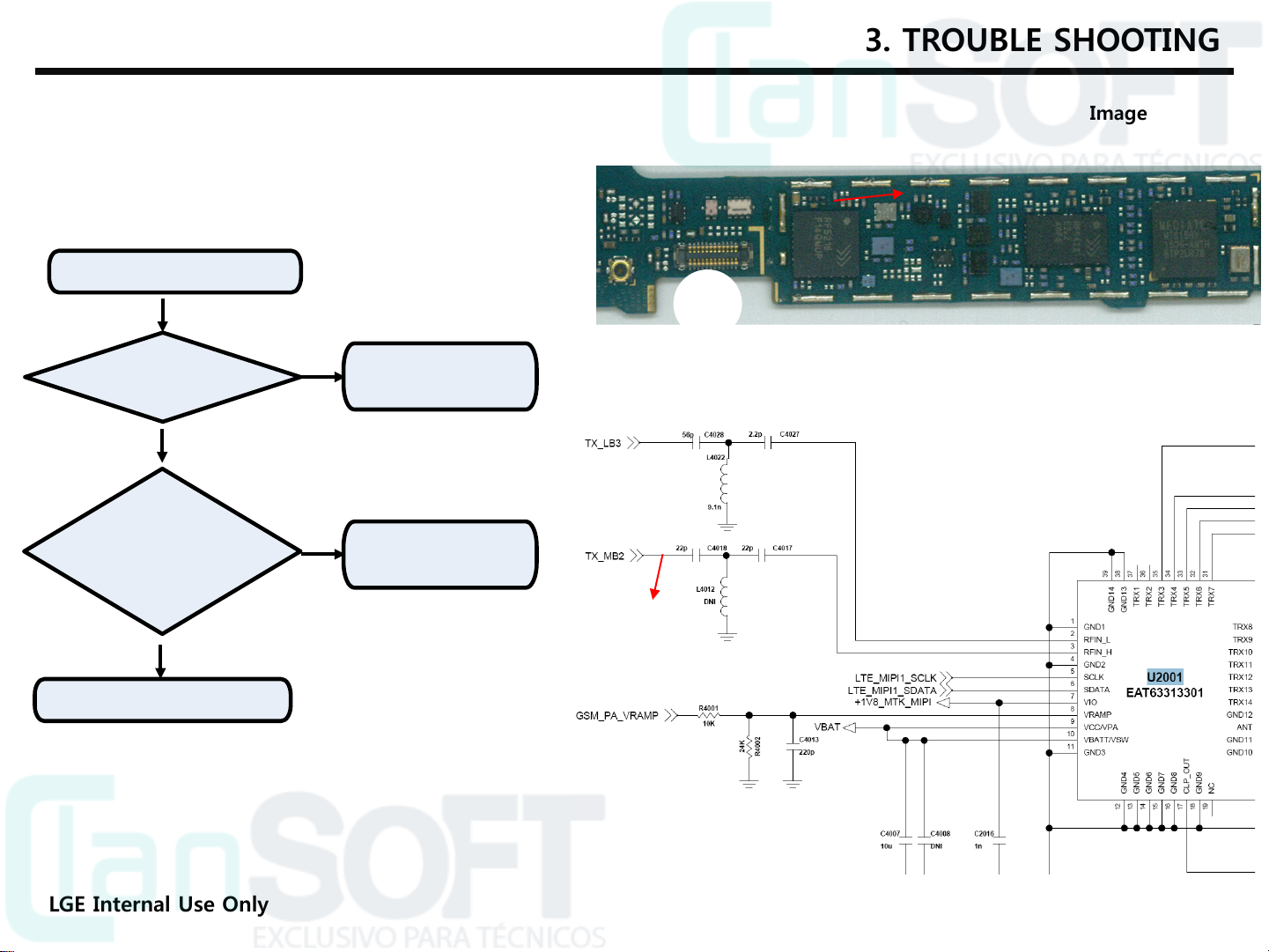
3. TROUBLE SHOOTING
10
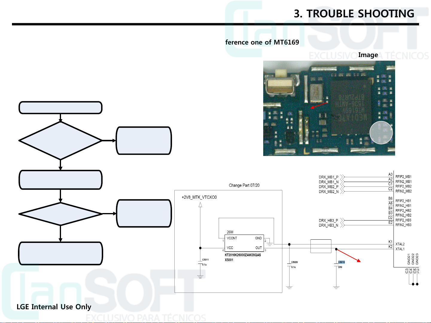
3.1 Checking XO Block
The out put frequency(26MHz) of VTCXO(X5001) is used as the reference one of MT6169
Checking Flow
Image
X5001
START
Check TP1
Is it 26MHz?
NO
Replace X5001 and then
check TP1
Is it 26MHz?
NO
The Problem may be
Logic part
Refer to Logic trouble shoot
YES
YES
XO Circuit is OK.
Check next step
XO Circuit is OK.
Check next step
TP1
Main
BOT
Circuit Diagram
TP1
LGE Internal Use Only
Copyright ⓒ 2016 LG Electronics. Inc. All right
reserved. Only training and service purposes
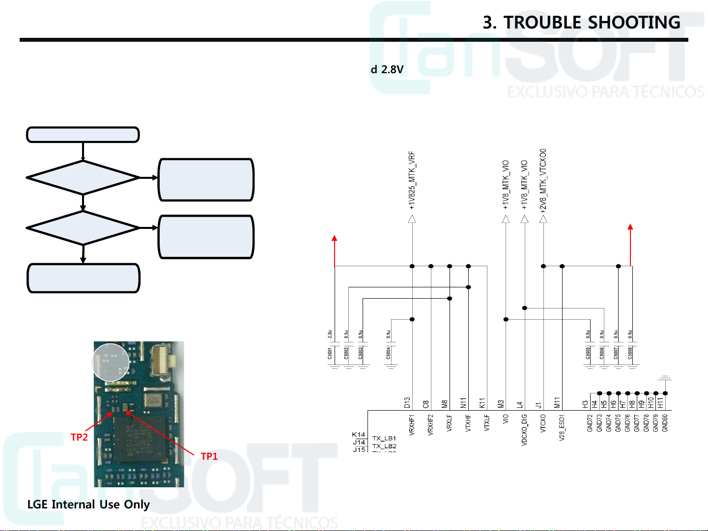
3.2 Checking Transceiver DC Power Supply Circuit Block
11
The MT6169 operating voltages used two voltage sources 1.8V and 2.8V
Checking Flow
3. TROUBLE SHOOTING
START
Check TP1
+1.8V_RF is OK?
YES
Check TP2
+2.8V_RF is OK?
YES
Check next step
Main
BOT
NO
NO
Image
The Problem may be
Logic part
Refer to
Logic trouble shoot
The Problem may be
Logic part
Refer to
Logic trouble shoot
Circuit Diagram
TP2
TP1
TP2
LGE Internal Use Only
TP1
Copyright ⓒ 2016 LG Electronics. Inc. All right
reserved. Only training and service purposes
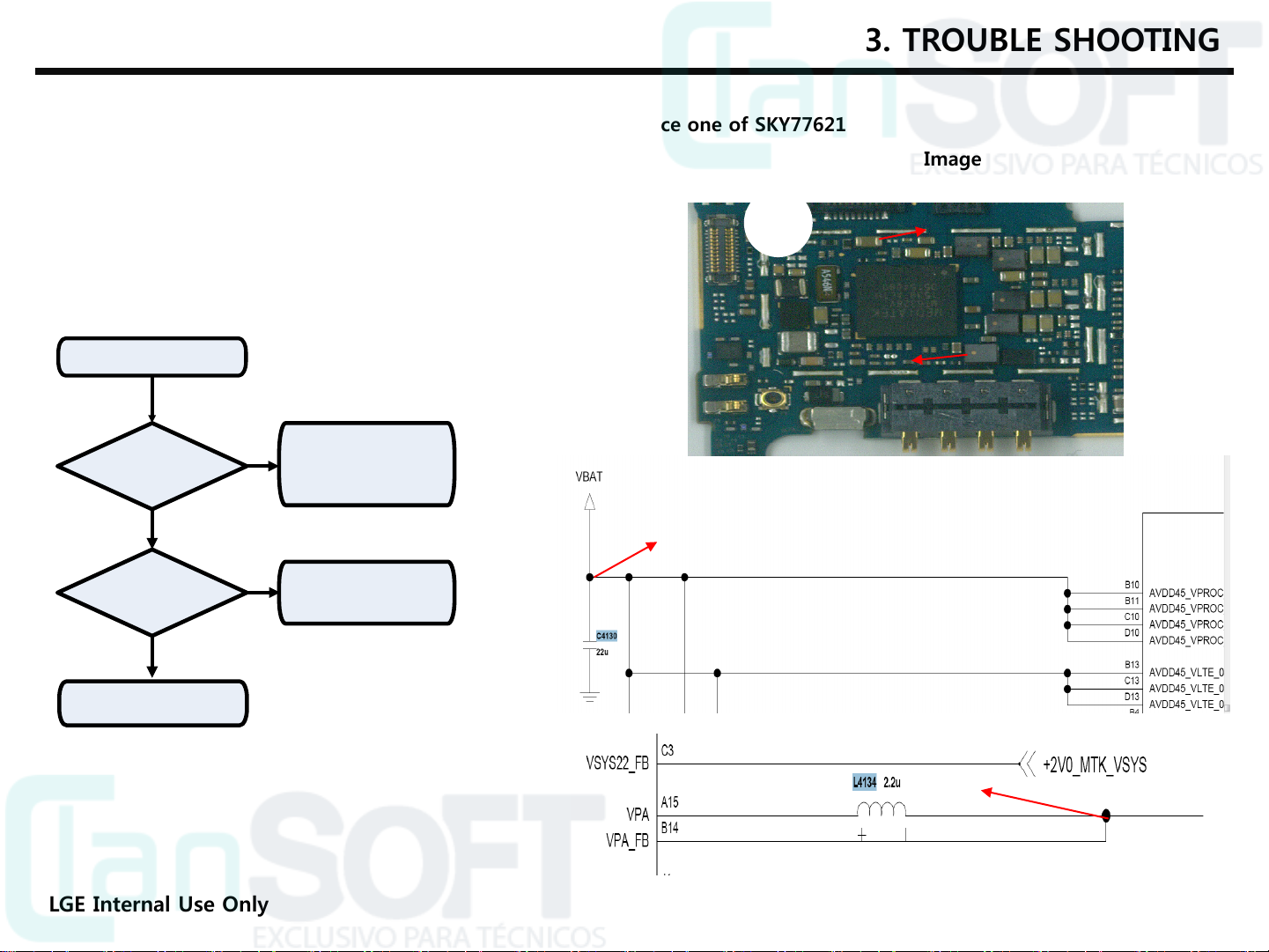
3.3 Checking DC-DC Block
12
The DC-DC(MT6325, U4100) output voltages is used as the reference one of SKY77621
Main
Bot
Checking Flow
3. TROUBLE SHOOTING
Image
TP1
U4100
START
Check TP1
VBAT is OK?
YES
Check TP2
0.5V ≤ TP2 ≤ 3.4V ?
YES
Check next step
The Problem may be
Logic part
Refer to Logic trouble
NO
Check U1400 Physical
Damage or soldering
NO
condition
shoot
TP2
Circuit Diagram
TP1
TP2
LGE Internal Use Only
Copyright ⓒ 2016 LG Electronics. Inc. All right
reserved. Only training and service purposes
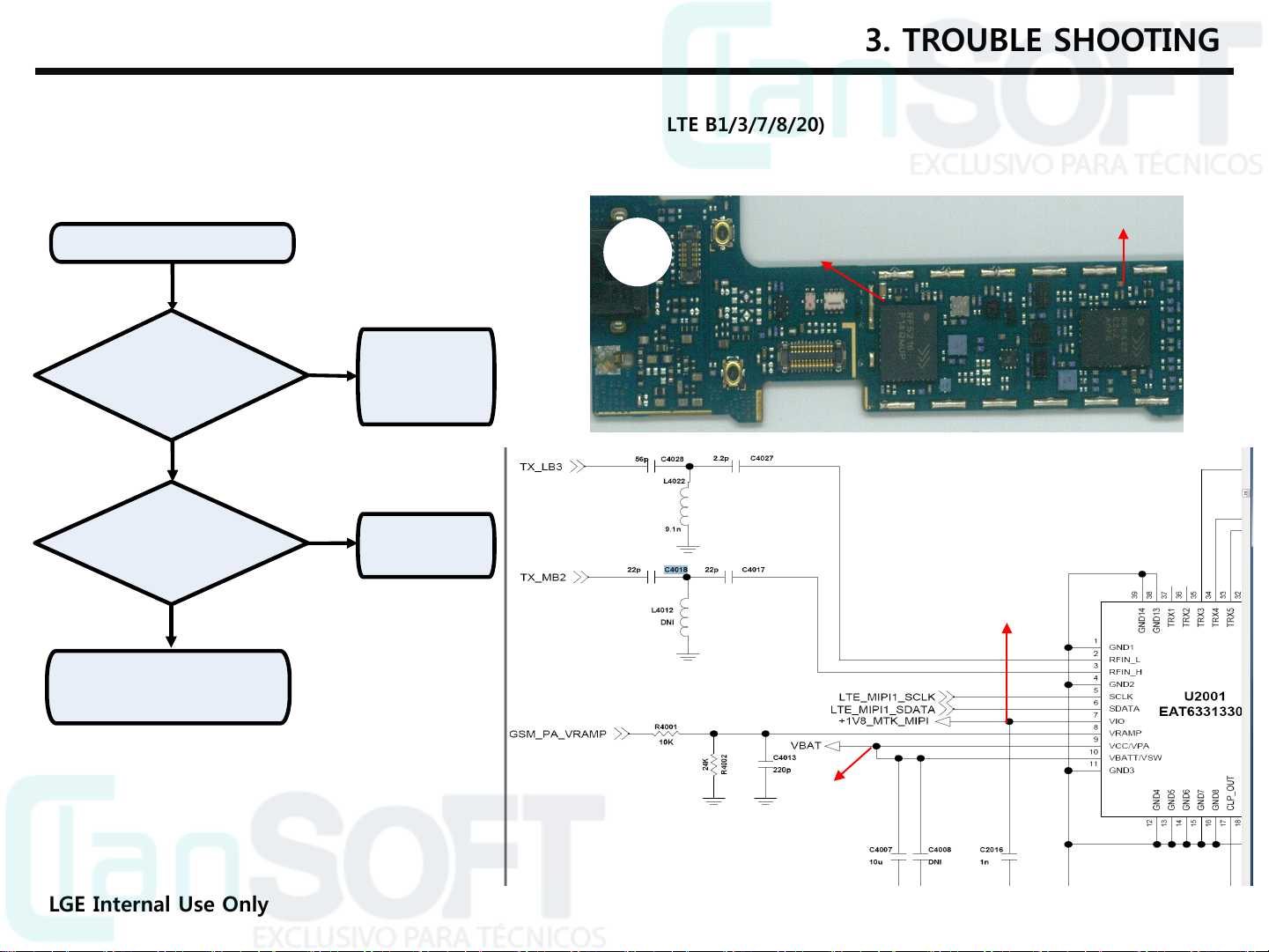
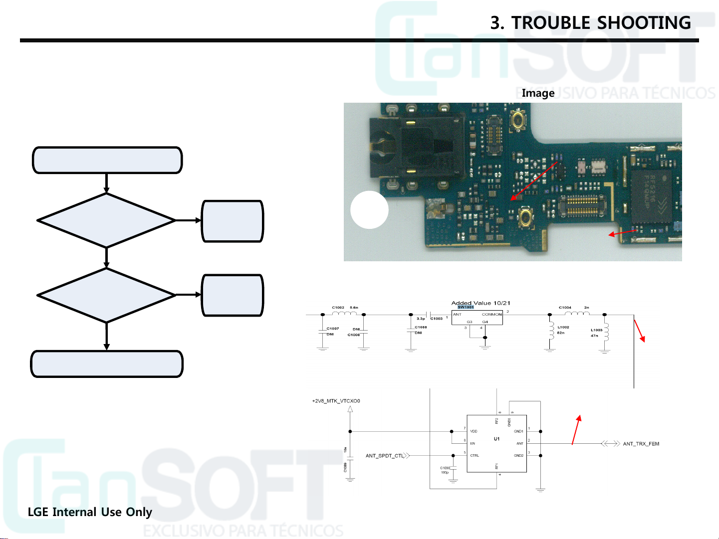
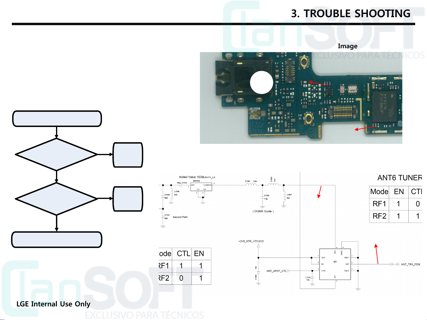
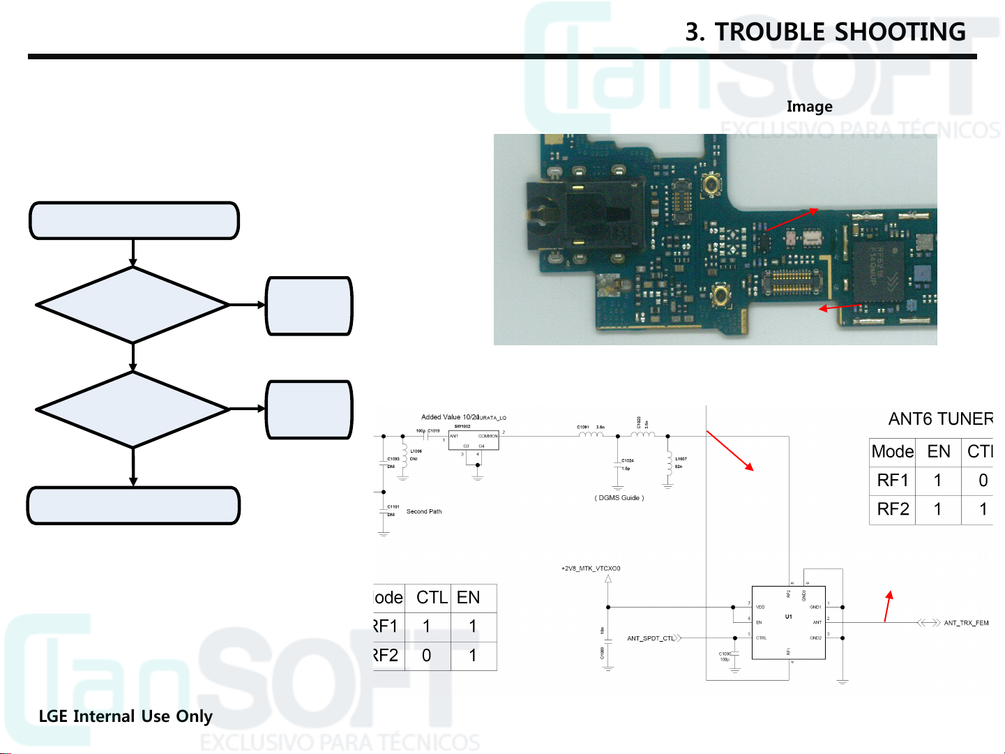
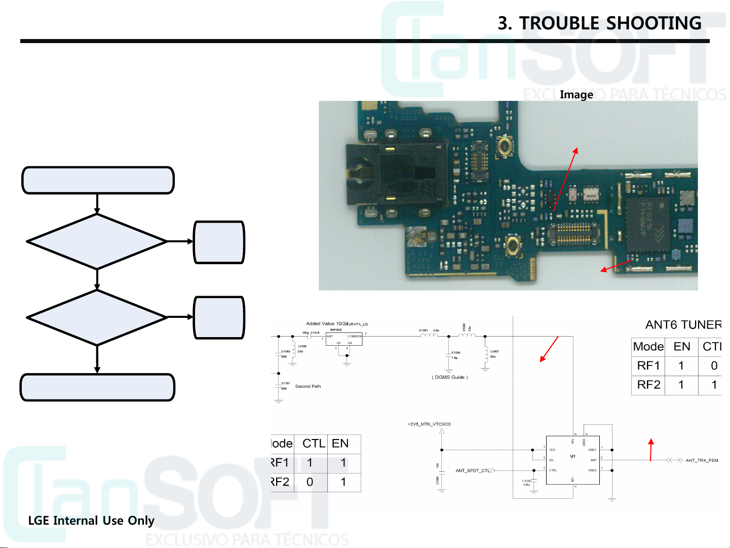
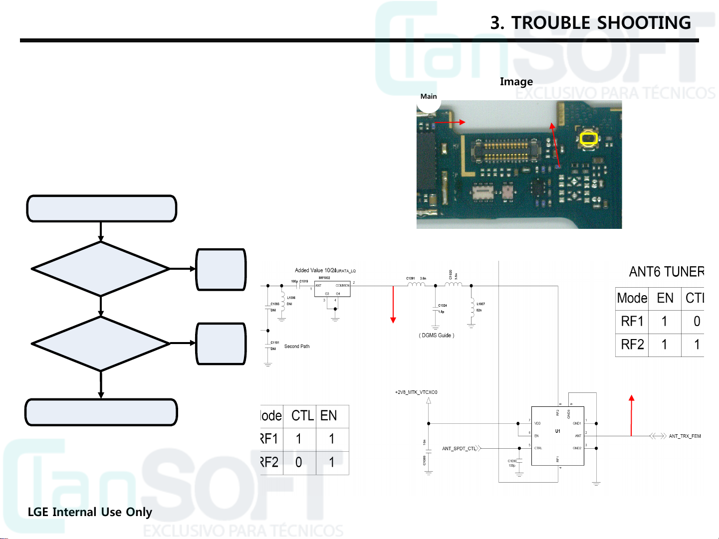
3.4 ASM(Antenna Switch Module) Block
13
3.4.1 Checking ANT #1 ASM (GSM 850/900/1800/1900), W B1/5/8, LTE B1/3/7/8/20)
3. TROUBLE SHOOTING
Checking Flow
START
Check TP1, TP2 High Level ?
(1.65V≤TP1 ≤2.0V)
(3.0V≤TP2 ≤4.6V)
YES
Check U2001 physical Damage
or soldering condition
OK?
NO
NOT GOOD
The Problem
may be Logic
part
Refer to Logic
trouble shoot
Replace U2001
Main
BOT
Image
TP1
TP2
U2100
Circuit Diagram
TP1
Check Next step
LGE Internal Use Only
TP2
Copyright ⓒ 2016 LG Electronics. Inc. All right
reserved. Only training and service purposes
3. TROUBLE SHOOTING
14
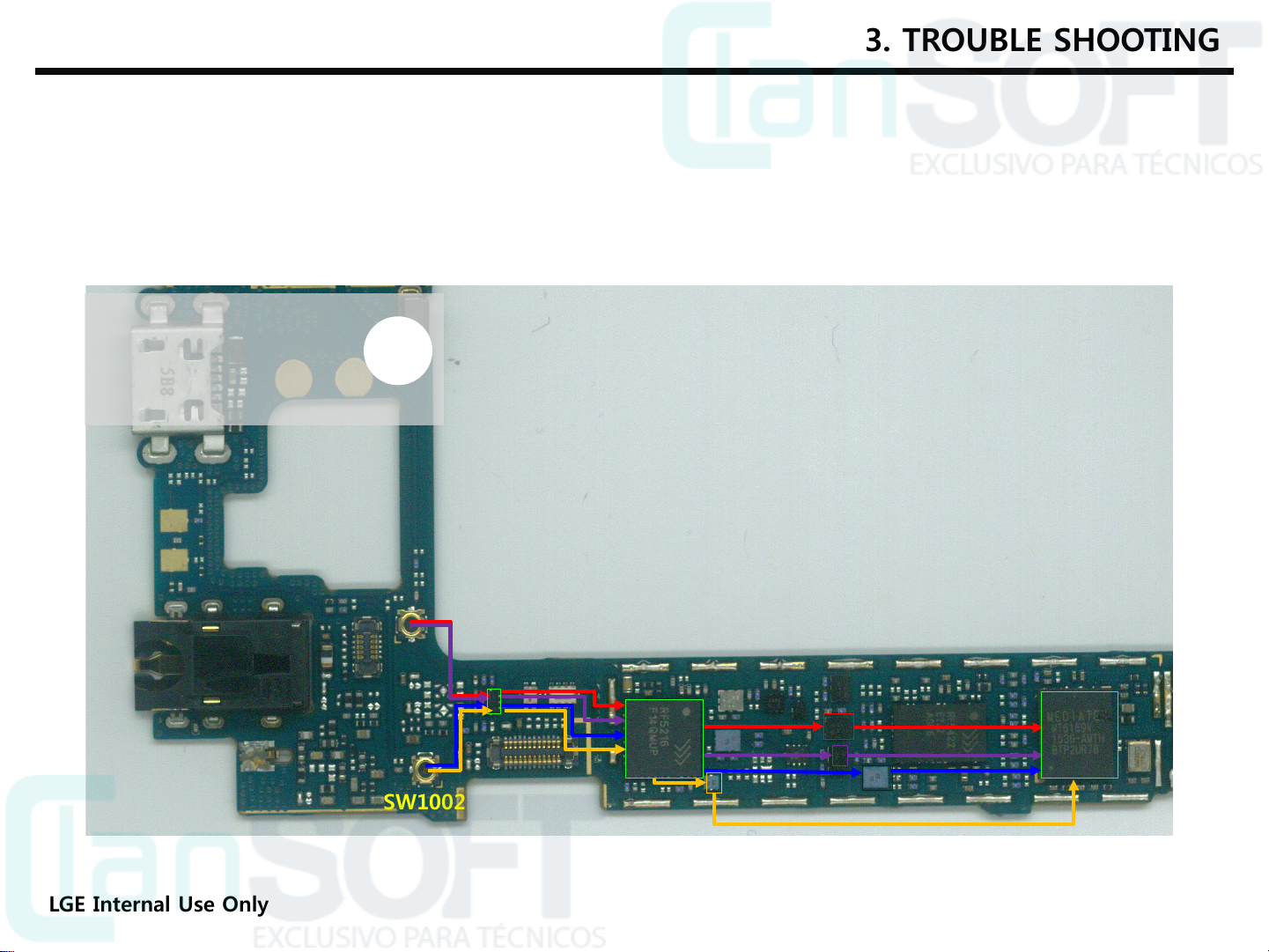
3.5 GSM RF PART
GSM RF Part support GSM850/900/1800/1900 with ASM, PAM, Transceiver component
Checking Flow
START
Check XO Block
Refer 3.1
Check Transceiver DC Power supply Block
Refer 3.2
Check DC-DC Block
Refer 3.3
LGE Internal Use Only
Check ASM Block
Refer 3.4
Check T/RX Block
Re-Download & Cal
Change the Board
Copyright ⓒ 2016 LG Electronics. Inc. All right
reserved. Only training and service purposes
3.5 GSM RF PART
15
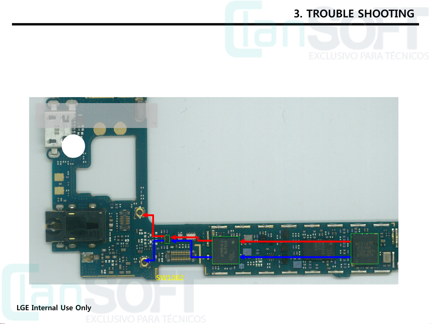
3.5.1 GSM RF Part RX RF PATH
1. GSM850 RX PATH
2. GSM900 RX PATH
3. GSM1800 RX PATH
4. GSM1900 RX PATH
3. TROUBLE SHOOTING
Image
Main
BOT
LGE Internal Use Only
SW1001
SW1002
Copyright ⓒ 2016 LG Electronics. Inc. All right
reserved. Only training and service purposes
3.5 GSM RF PART
16
3.5.2 Checking RF Signal RX path(SW, GSM850/900)
Checking Flow
START
3. TROUBLE SHOOTING
Image
Check TP1 Signal exist?
YES
Check TP2 Signal exist?
YES
Check next step
NO
NO
Check
SW1001
Soldering
Check U1
Soldering
Main
BOT
TP1
TP2
Circuit Diagram
TP1
TP2
LGE Internal Use Only
Copyright ⓒ 2016 LG Electronics. Inc. All right
reserved. Only training and service purposes
3.5 GSM RF PART
17
3.5.3 Checking RF Signal RX path(GSM850/900)
3. TROUBLE SHOOTING
START
Check TP1/2 Signal exist?
YES
Check TP3/4 Signal exist?
YES
Check Transceiver
physical damage
or soldering condition
Checking Flow
NO
NO
NOT GOOD
Replace U2100
Check Component
above RF signal path
Replace U5001
Image
Main
BOT
TP1
TP2
TP2
TP4
TP1
TP3
Circuit Diagram
TP3
Check next step
LGE Internal Use Only
OK?
TP4
Copyright ⓒ 2016 LG Electronics. Inc. All right
reserved. Only training and service purposes
3.5 GSM RF PART
18
3. TROUBLE SHOOTING
3.5.4 Checking RF Signal RX path(SW, GSM1800/1900)
Checking Flow
START
Check TP1 Signal exist?
YES
Check TP2 Signal exist?
NO
NO
Check
SW1002
Soldering
Check
U1
Soldering
Main
BOT
TP1
SW1002
Circuit Diagram
TP1
Image
TP2
Check next step
LGE Internal Use Only
YES
TP2
Copyright ⓒ 2016 LG Electronics. Inc. All right
reserved. Only training and service purposes
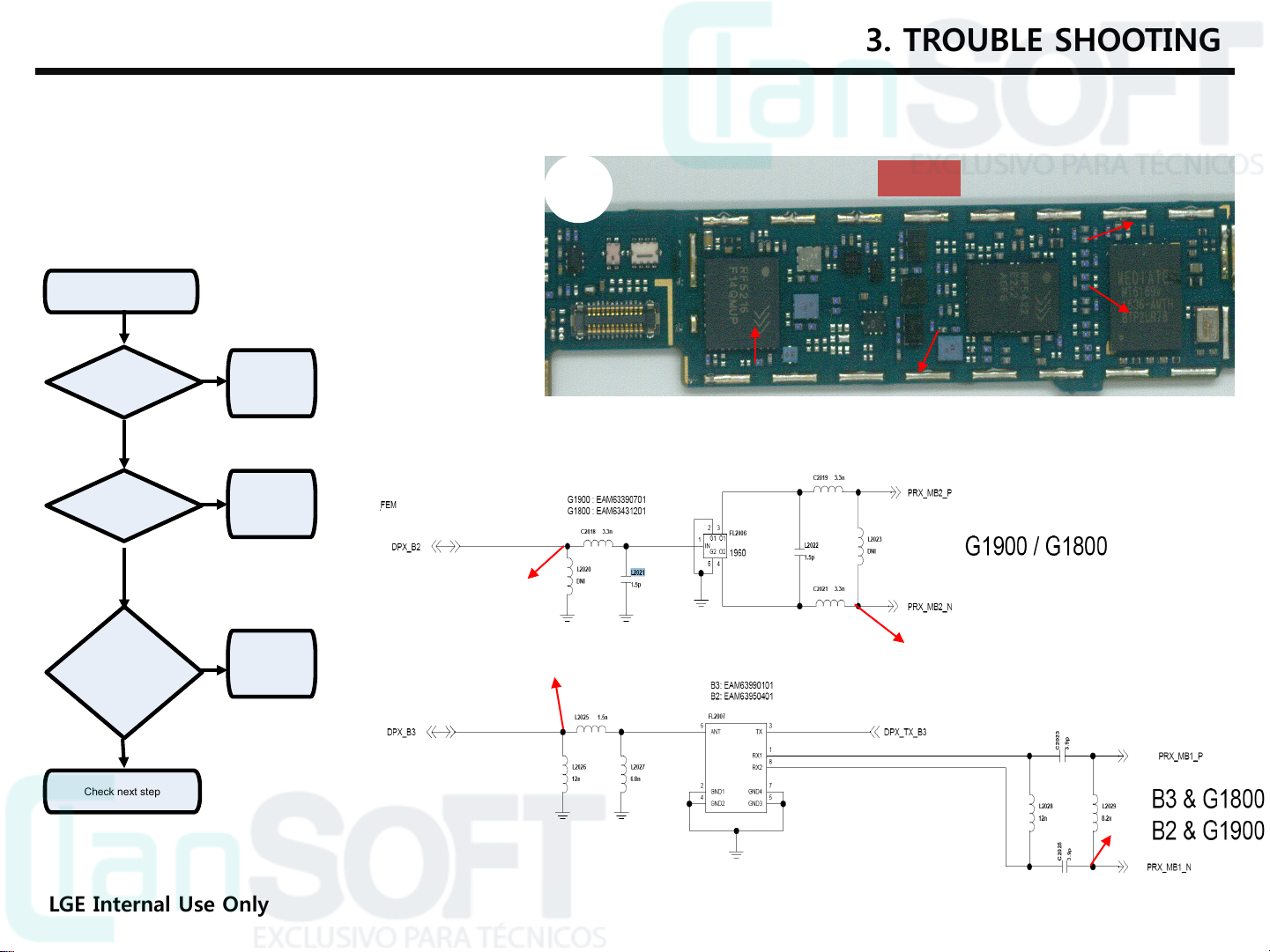
3.5 GSM RF PART
19
3.5.5 Checking RF Signal RX path(GSM1800/1900)
3. TROUBLE SHOOTING
Checking Flow
START
Check TP1/2 Signal exist?
YES
Check TP3/4 Signal exist?
YES
Check Transceiver
physical damage
or soldering condition
NO
NO
NOT
GOOD
Replace
U2100
Check
Component
above RF
signal path
Replace
U5001
TP1
TP2
Main
BOT
TP1
Circuit Diagram
Image
TP4
TP3
TP2
TP3
OK?
Check next step
LGE Internal Use Only
TP4
Copyright ⓒ 2016 LG Electronics. Inc. All right
reserved. Only training and service purposes
3.5 GSM RF PART
20
3.5.6 GSM RF Part TX RF PATH
1. GSM850/900 TX PATH
2. GSM1800/1900 TX PATH
Main
BOT
3. TROUBLE SHOOTING
LGE Internal Use Only
SW1001
SW1002
Copyright ⓒ 2016 LG Electronics. Inc. All right
reserved. Only training and service purposes
3.5 GSM RF PART
21
3.5.7 Checking GSM PAM DC Power Circuit
Checking Flow
START
Main
BOT
TP1
3. TROUBLE SHOOTING
Image
TP2
Check TP1
+VPWR OK?
YES
Check TP2/3
1.65V≤TP2≤1.95V?
0.5V≤TP3≤4.6V?
YES
Check Next step
NO
NO
The Problem may be
Other part
Check Logic part
Check DC-DC Power
Block
Refer to 3.3
TP3
TP3
Circuit Diagram
TP1
TP2
LGE Internal Use Only
Copyright ⓒ 2016 LG Electronics. Inc. All right
reserved. Only training and service purposes
3.5 GSM RF PART
22
3. TROUBLE SHOOTING
3.5.8 Checking RF Signal TX path(SW, GSM850/900)
Checking Flow
START
Check TP1 Signal exist?
YES
Check TP2 Signal exist?
YES
Check next step
NO
NO
Check
SW1001
Soldering
Check
U1 Soldering
Image
SW1001
TP1
TP2
Circuit Diagram
TP1
LGE Internal Use Only
TP2
Copyright ⓒ 2016 LG Electronics. Inc. All right
reserved. Only training and service purposes
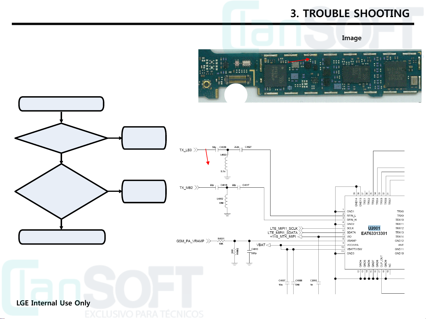
3.5 GSM RF PART
23
3.5.9 Checking RF Signal TX path(GSM850/900)
3. TROUBLE SHOOTING
Image
TP1
U5001
Checking Flow
START
NO
Check TP1
If GSM850/900 Over 3.8dBm?
NO
Check Transceiver
physical damage
or soldering condition
OK?
Check next step
U2001
Main
BOT
Replace U2001
YES
TP1
Replace U5001
NOT GOOD
LGE Internal Use Only
Copyright ⓒ 2016 LG Electronics. Inc. All right
reserved. Only training and service purposes
3.5 GSM RF PART
24
3.5.10 Checking RF Signal TX path(SW, GSM1800/1900)
Checking Flow
START
3. TROUBLE SHOOTING
Image
TP1
Check TP1 Signal exist?
Check TP2 Signal exist?
Check next step
LGE Internal Use Only
YES
YES
NO
NO
Check
SW1002
Soldering
Check
U1
Soldering
SW1002
Circuit Diagram
TP1
Copyright ⓒ 2016 LG Electronics. Inc. All right
reserved. Only training and service purposes
TP2
TP2
3.5 GSM RF PART
25
3.5.11 Checking RF Signal TX path(GSM1800/1900)
3. TROUBLE SHOOTING
Image
TP1
Checking Flow
START
NO
Check TP1
If GSM850/900 Over 2.5dBm?
NO
Check Transceiver
physical damage
or soldering condition
OK?
Check next step
YES
NOT GOOD
U2001 U5001
Main
BOT
Replace U2001
Circuit Diagram
Replace U5001
TP1
LGE Internal Use Only
Copyright ⓒ 2016 LG Electronics. Inc. All right
reserved. Only training and service purposes
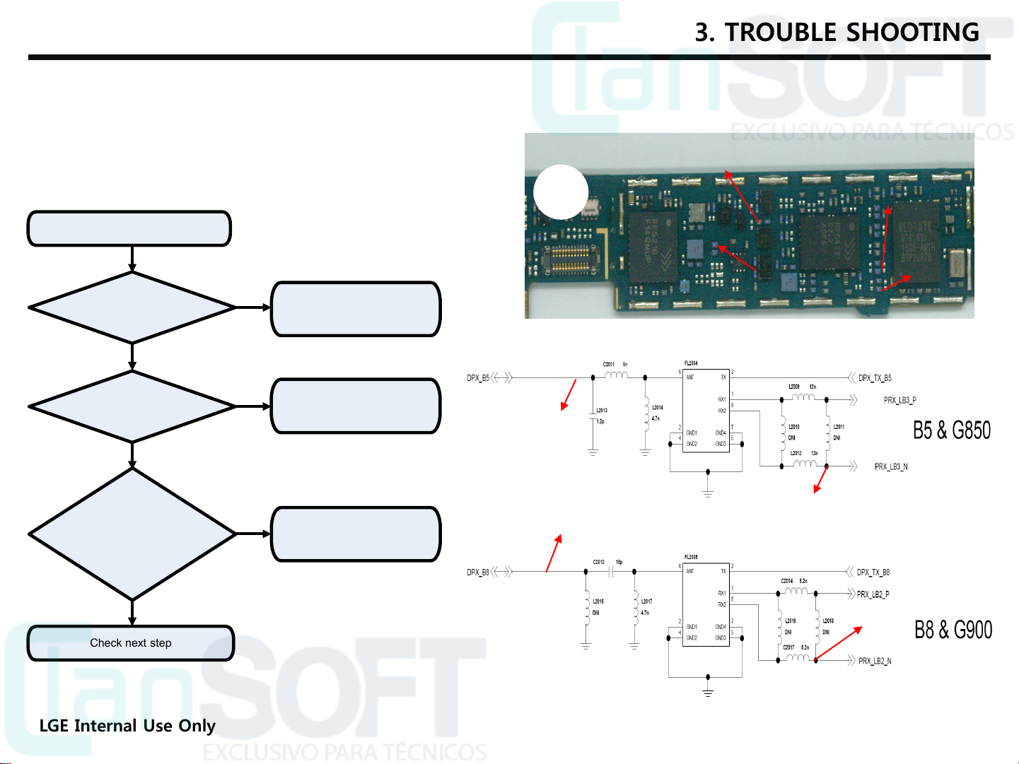
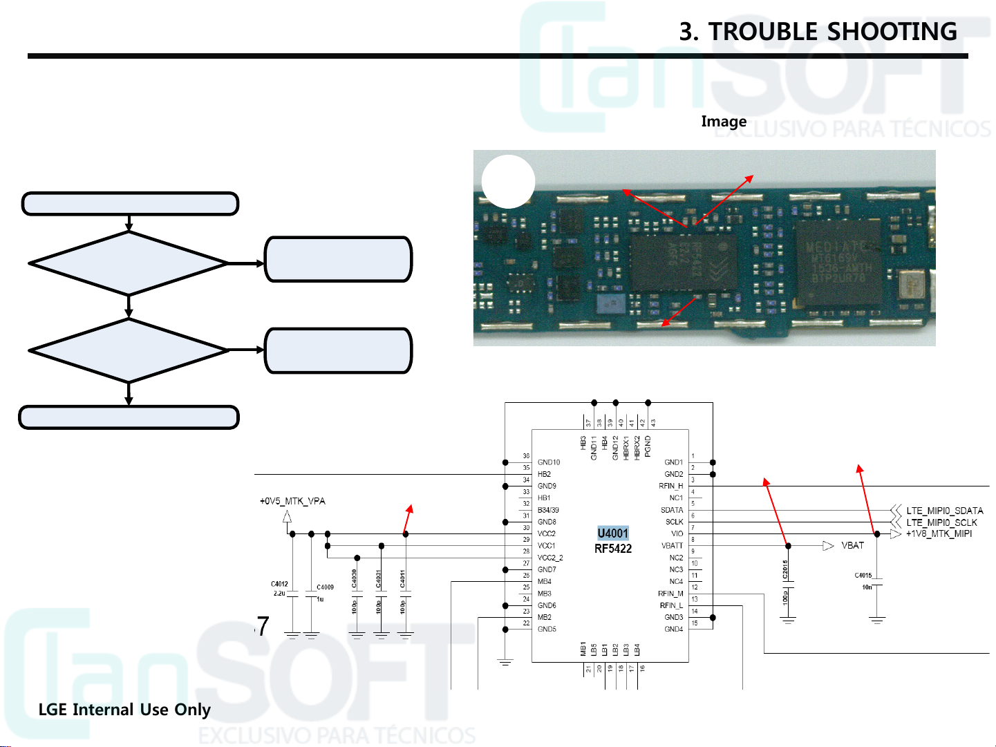
3.6 WCDMA RF PART
26
WCDMA RF Part support WCDMA B1/5/8 with ASM, PAM, Transceiver component
Checking Flow
START
Check XO Block
Refer 3.1
Check Transceiver DC Power supply Block
Refer 3.2
Check DC-DC Block
Refer 3.3
3. TROUBLE SHOOTING
LGE Internal Use Only
Check ASM Block
Refer 3.4
Check T/RX Block
Re-Download & Cal
Change the Board
Copyright ⓒ 2016 LG Electronics. Inc. All right
reserved. Only training and service purposes
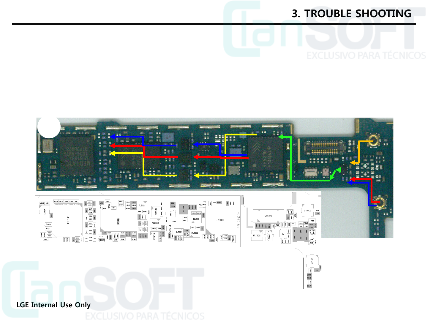
3.6 WCDMA RF PART
27
3.6.1 WCDMA RF Part RX RF PATH
Image
1. WCDMA B1 RX PATH 2. WCDMA B5 RX PATH
3. WCDMA B8 RX PATH 4. RX COMMON PATH
Main
BOT
3. TROUBLE SHOOTING
SW1002
LGE Internal Use Only
SW1001
Copyright ⓒ 2016 LG Electronics. Inc. All right
reserved. Only training and service purposes
3.6 WCDMA RF PART
28
3.6.2 Checking RF Signal RX path(SW, WCDMA B1)
Checking Flow
START
Check TP1 Signal exist?
YES
NO
Check
SW1002
Soldering
SW1002
Main
BOT
3. TROUBLE SHOOTING
Image
TP1
TP2
Circuit Diagram
SW1002
Check TP2 Signal exist?
Check next step
LGE Internal Use Only
YES
NO
Check
U1
Soldering
TP1
TP2
U1
Copyright ⓒ 2016 LG Electronics. Inc. All right
reserved. Only training and service purposes
3.6 WCDMA RF PART
29
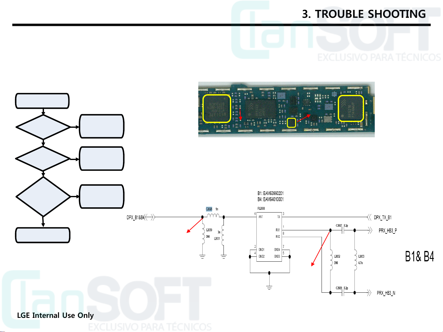
3.6.3 Checking RF Signal RX path(WCDMA B1)
Checking Flow
START
U5001
3. TROUBLE SHOOTING
Image
TP1
U2001
Check TP1 Signal exist?
YES
Check TP2 Signal exist?
YES
Check Transceiver
physical damage
or soldering condition
OK?
Check next step
NO
NO
NOT GOOD
Replace FL2001
Replace FL2008
Replace U5001
TP2
FL2008
Circuit Diagram
TP1
TP2
LGE Internal Use Only
Copyright ⓒ 2016 LG Electronics. Inc. All right
reserved. Only training and service purposes
3.6 WCDMA RF PART
30
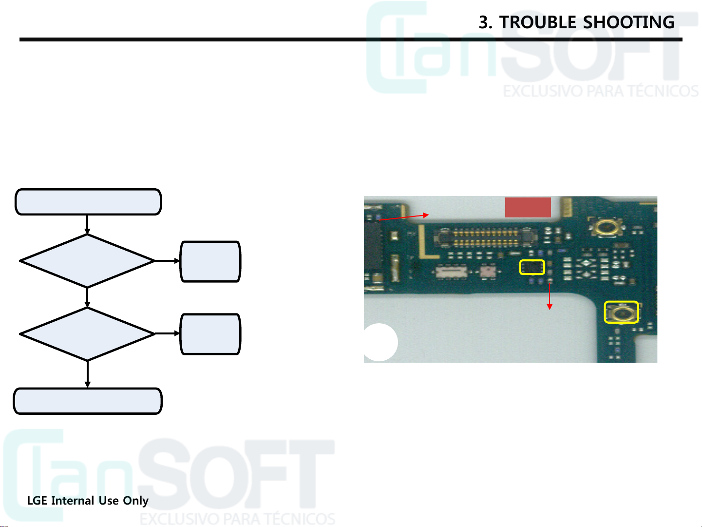
3.6.4 Checking RF Signal RX path(SW, WCDMA B5/8)
Checking Flow
START
TP2
3. TROUBLE SHOOTING
Image
Check TP1 Signal exist?
Check TP2 Signal exist?
Check next step
LGE Internal Use Only
YES
YES
NO
NO
Check
SW1002
Soldering
Check U1
Soldering
Main
BOT
U1
TP1
SW1002
Copyright ⓒ 2016 LG Electronics. Inc. All right
reserved. Only training and service purposes
 Loading...