

Page 1

COLOR MONIT OR
SER VICE MANUAL
Website:http://biz.LGservice.com
E-mail:http://www.LGEservice.com/techsup.html
CAUTION
BEFORE SERVICING THE UNIT,
READ THE SAFETY PRECAUTIONS IN THIS MANUAL.
CHASSIS NO. : CL-18
F ACTORY MODEL: LB565T
MODEL: LCD 575LE (LB565T -EA)
*( ) ID LABEL MODEL No.
Page 2
CONTENTS
SPECIFICATIONS
- 2 -
1. LCD CHARACTERISTICS
Type : TFT XGA LCD
Size : 15 inch (38.1cm)
Pixel Pitch : 0.297mm (H) x 0.297mm (V)
Electrical Interface : LVDS Interface
Color Depth : 6-bits/ 16,194,277 colors
Active Video Area : 304.1mm (H) x 228.1mm (V)
Surface Treatment : Anti-Glare, Hard Coating (3H)
Backlight Unit : Bottom edge side 2CCFL
2. OPTICAL CHARACTERISTICS
2-1. Viewing Angle by Contrast Ratio
≥
10
Left : 50° typ., 50° min.
Right : 60° typ., 60° min.
Top : 40° typ., 40°min.
Bottom : 55° typ., 45° min.
2-2. Luminance : 200 cd/m
2
typ.
2-3. Angle at Half Luminance
Left : 70° min.
Right : 70° min.
Top : 40° min.
Bottom : 70° min.
2-4. Contrast Ratio : 250 typ.
3. SIGNAL (Refer to the Timing Chart)
3-1. Sync Signal
1) Type : Separate Sync. (Horizontal & Vertical)
2) Input Voltage Level: Low=0~0.8V, High=2.1~5.5V
3) Sync Polarity : Positive or Negative
3-2. Video Input Signal
1) Type : R, G, B Analog
2) Voltage Level : 0~0.714 V
a) Color 0, 0 : 0 Vp-p
b) Color 7, 0 : 0.467 Vp-p
c) Color 15, 0 : 0.714 Vp-p
3) Input Impedance : 75 Ω
3-3. Operating Frequency
Horizontal : 31 ~ 61 kHz
Vertical : 56 ~ 75 Hz
4. POWER SUPPLY
4-1. Power Adaptor
Input : AC 100~240V, 50/60Hz 1.2A
Output : DC 12V 3.0A
4-2. Power Consumption
5. ENVIRONMENT
5-1. Operating Temperature: 10°C~35°C (50°F~95°F)
(Ambient)
5-2. Relative Humidity : 5%~95%
(Non-condensing)
5-3. Altitude : 0~10,000ft (3,030m)
6. DIMENSIONS (with TILT/SWIVEL)
Width : 394 mm (15.51'')
Depth : 161.8 mm (6.37'')
Height : 378.7 mm (14.91'')
7. WEIGHT (with TILT/SWIVEL)
Net. Weight : 4.8 kg (10.58 lbs)
Gross Weight : 6.9 kg (15.21 l
bs)
SPECIFICATIONS ................................................... 2
PRECAUTIONS ....................................................... 3
TIMING CHART ....................................................... 4
OPERATING INSTRUCTIONS ................................ 5
WIRING DIAGRAM ................................................. 6
BLOCK DIAGRAM ................................................... 7
DESCRIPTION OF BLOCK DIAGRAM.....................8
ADJUSTMENT ........................................................ 9
TROUBLESHOOTING GUIDE .............................. 10
PRINTED CIRCUIT BOARD................................... 14
EXPLODED VIEW...................................................17
REPLACEMENT PARTS LIST ...............................19
PIN CONFIGURATION............................................23
SCHEMATIC DIAGRAM......................................... 24
MODE
POWER ON (NORMAL)
STAND-BY
SUSPEND
OFF
POWER OFF
H/V SYNC
ON/ON
OFF/ON
ON/OFF
OFF/OFF
-
POWER CONSUMPTION
less than 36 W
less than 3 W
less than 3 W
less than 3 W
less than 3 W
LED COLOR
GREEN
YELLOW
YELLOW
YELLOW
OFF
VIDEO
ACTIVE
OFF
OFF
OFF
-
Page 3

- 3 -
WARNING FOR THE SAFETY-RELATED COMPONENT.
• There are some special components used in LCD
monitor that are important for safety. These parts are
marked on the schematic diagram and the
replacement parts list. It is essential that these critical
parts should be replaced with the manufacturer’s
specified parts to prevent electric shock, fire or other
hazard.
• Do not modify original design without obtaining written
permission from manufacturer or you will void the
original parts and labor guarantee.
TAKE CARE DURING HANDLING THE LCD MODULE
WITH BACKLIGHT UNIT.
• Must mount the module using mounting holes arranged
in four corners.
• Do not press on the panel, edge of the frame strongly
or electric shock as this will result in damage to the
screen.
• Do not scratch or press on the panel with any sharp
objects, such as pencil or pen as this may result in
damage to the panel.
• Protect the module from the ESD as it may damage the
electronic circuit (C-MOS).
• Make certain that treatment person’s body are
grounded through wrist band.
• Do not leave the module in high temperature and in
areas of high humidity for a long time.
• The module not be exposed to the direct sunlight.
• Avoid contact with water as it may a short circuit within
the module.
• If the surface of panel become dirty, please wipe it off
with a softmaterial. (Cleaning with a dirty or rough cloth
may damage the panel.)
WARNING
BE CAREFUL ELECTRIC SHOCK !
• If you want to replace with the new backlight (CCFL) or
inverter circuit, must disconnect the AC adapter
because high voltage appears at inverter circuit about
650Vrms.
• Handle with care wires or connectors of the inverter
circuit. If the wires are pressed cause short and may
burn or take fire.
PRECAUTION
CAUTION
Please use only a plastic screwdriver to protect yourself
from shock hazard during service operation.
Page 4
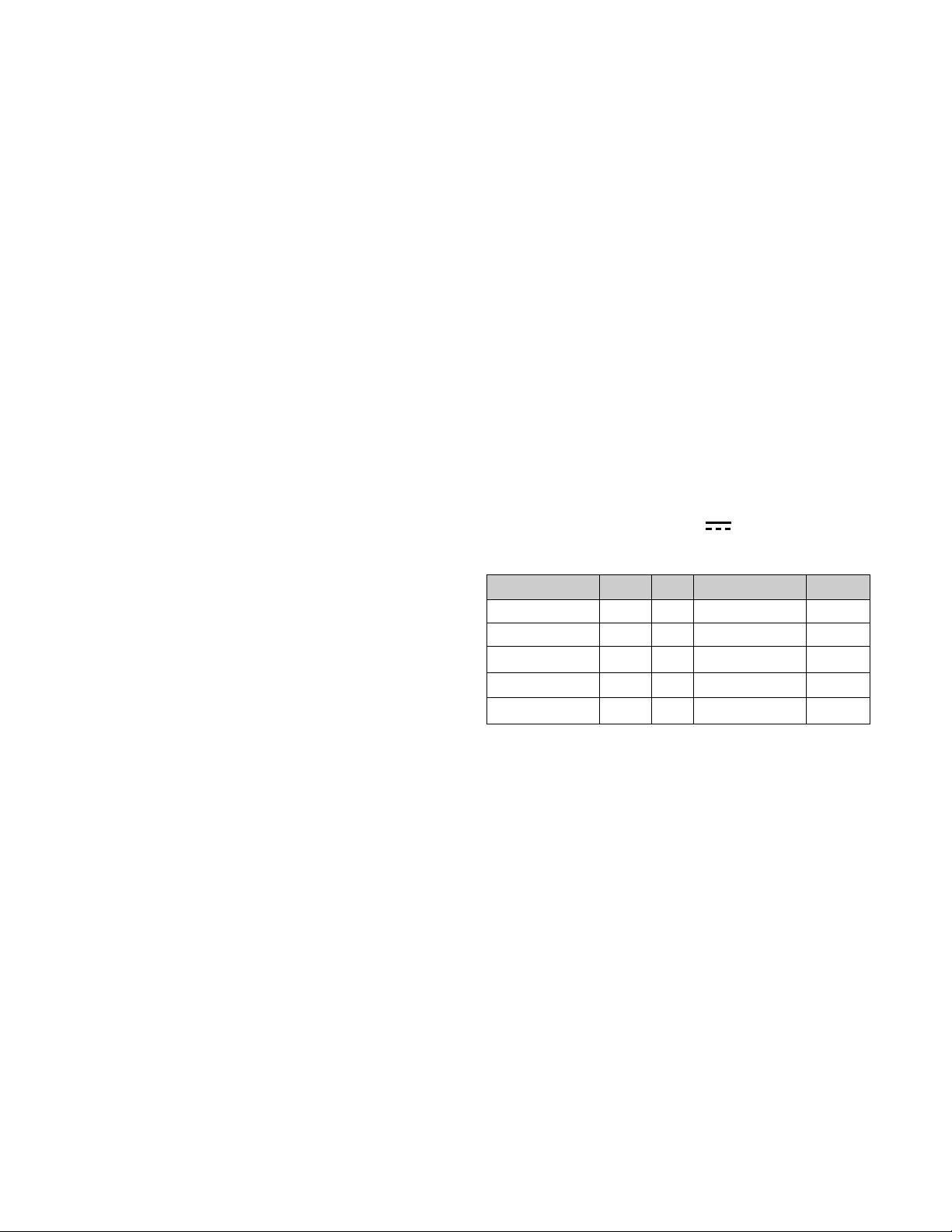
TIMING CHART
- 4 -
VIDEO
SYNC
B
D
C
F
E
A
H / V
H (Pixels)
V (Lines)
H (Pixels)
V (Lines)
H (Pixels)
V (Lines)
H (Pixels)
V (Lines)
H (Pixels)
V (Lines)
H (Pixels)
V (Lines)
H (Pixels)
V (Lines)
H (Pixels)
V (Lines)
H (Pixels)
V (Lines)
H (Pixels)
V (Lines)
H (Pixels)
V (Lines)
H (Pixels)
V (Lines)
H (Pixels)
V (Lines)
H (Pixels)
V (Lines)
Sync
Polarity
+
–
–
+
–
–
–
–
–
–
–
–
+
+
+
+
+
+
+
+
–
–
–
–
–
–
+
+
Dot
Clock
25.175
28.322
25.175
30.24
31.5
31.5
36.0
40.0
50.0
49.5
57.2832
65
75
78.75
Frequency
31.468 KHz
70.0 Hz
31.468 KHz
70.0 Hz
31.469 KHz
60.0 Hz
35.00 KHz
66.67 Hz
37.861 KHz
72.8 Hz
37.50 KHz
75.0 Hz
35.156 KHz
56.25 Hz
37.879 KHz
60.3 Hz
48.077 KHz
72.188 Hz
46.875 KHz
75.0 Hz
49.725 KHz
74.55 Hz
48.363 KHz
60.0 Hz
56.476 KHz
70.0 Hz
60.023 KHz
75.0 Hz
Resolution
640 x 350
720 x 400
(TEXT)
640 x 480
640 x 480
640 x 480
640 x 480
800 x 600
800 x 600
800 x 600
800 x 600
832 x 624
(MAC)
1024 x 768
1024 x 768
1024 x 768
Total
Period
( E )
800
449
900
449
800
525
864
525
832
520
840
500
1024
625
1056
628
1040
666
1056
625
1152
667
1344
806
1328
806
1312
800
Video
Active
Time ( A )
640
350
720
400
640
480
640
480
640
480
640
480
800
600
800
600
800
600
800
600
832
624
1024
768
1024
768
1204
768
Blanking
Time
( B )
160
99
180
49
160
45
224
45
192
40
200
20
224
25
256
28
240
66
256
25
320
43
320
38
304
38
288
32
Sync
Duration
( D )
96
2
108
2
96
2
64
3
40
3
64
3
72
2
128
4
120
6
80
3
64
3
136
6
136
6
96
3
Back
Porch
( F )
48
60
55
34
48
33
96
39
128
28
120
16
128
22
88
23
64
23
160
21
224
39
160
29
144
29
176
28
Front
Porch
( C )
16
37
17
13
16
10
64
3
24
9
16
1
24
1
40
1
56
37
16
1
32
1
24
3
24
3
16
1
MODE
1
2
3
4
5
6
7
8
9
10
11
12
13
14
Page 5
- 5 -
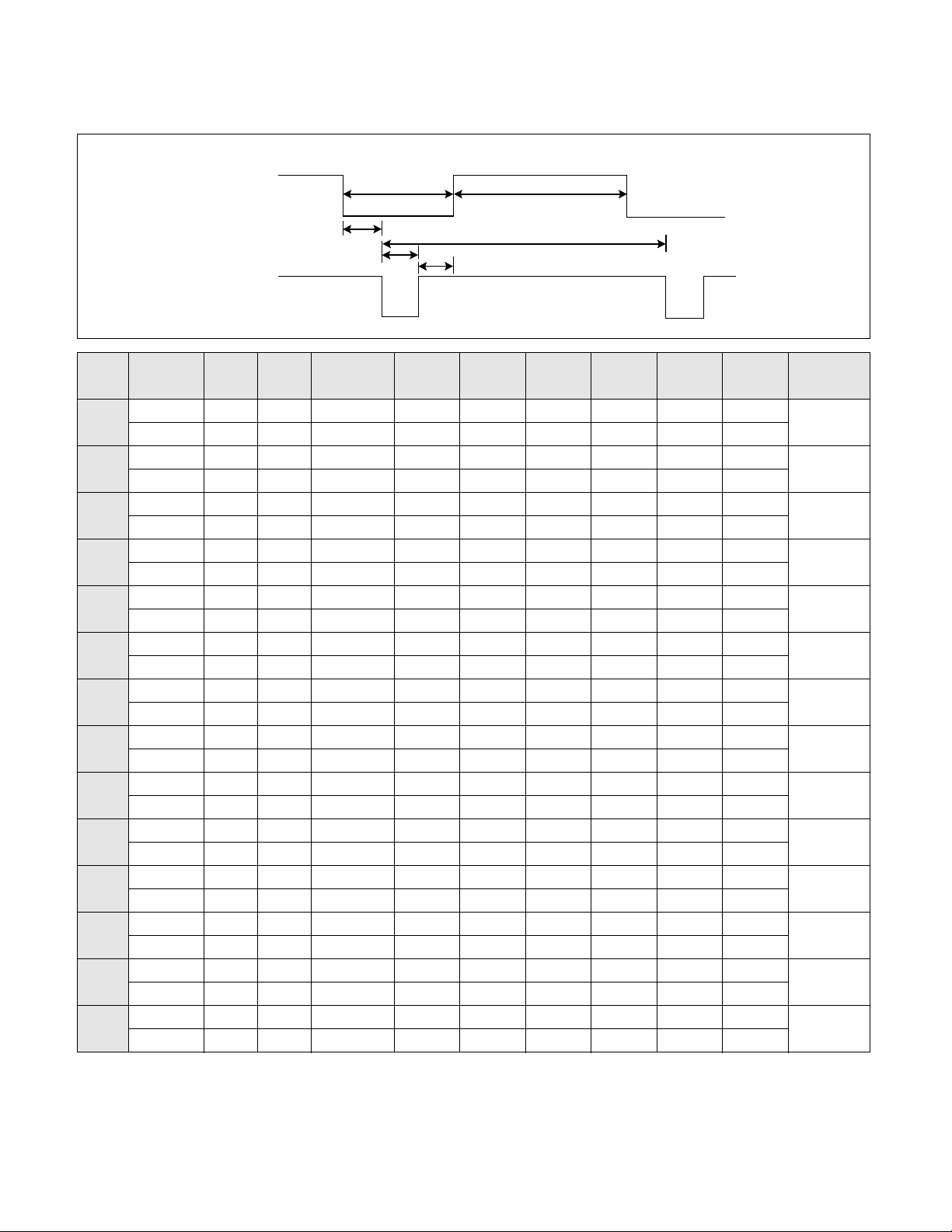
OPERATING INSTRUCTIONS
FRONT VIEW REAR VIEW
Front Control Panel
24V
AUDIO
DC OUT
AUDIO
DC OUT
1. Power ON/OFF Button
This button is used to turn the monitor ON and OFF.
2. Power Indicator
This indicator lights up green when the monitor
perates
normally. If the monitor is in DPM (Energy Saving)
mode (stand-by/ suspend/power off), this indicator color
changes to orange.
3. AUTO/SET Button
Use this button to enter a selection in the on screen display.
4. OSD Selection/Adjustment Buttons
Use these buttons to choose or adjust items in the on screen
display.
5. OSD Button
Use this button to enter or exit the on screen display.
Stand Cover
DC Power Connecter
-
+
D-Sub Signal Connector
Power ON/OFF Button
Power (DPMS) Indicator
Front Control Panel
<Shortcut Keys>
• Brightness and Contrast can be adjusted
directly without entering the On Screen
Display (OSD) system. Touch the
buttons to adjust the settings and then the
OSD button to save all changes. The
Brightness and Contrast functions are also
available in the On Screen Display (OSD)
menu.
* AUTO adjustment function
Touch the AUTO/SET button before
using OSD menu. This button is for the
automatic adjustment of the screen
position, clock and phase.
Note: Some signal from some graphics boards may not function
properly. If the results are unsatisfactory, adjust your monitor’s
Position, Clock and Phase manually.
PROCESSING
AUTO CONFIGURATION
OSD Selection/Adjustment
Buttons
AUTO/SET Buttons
Power ON/OFF Button
1
Power (DPMS) Indicator
23
OSD Buttons
54
100
100
Page 6
- 6 -
WIRING DIAGRAM
CN2
CN1
J4
J5
J10
J4
J11
J10
Connector Ass’y P/N:
6631T1 1012R
Connector Ass’y P/N:
6631T12002B
Connector Ass’y P/N:
6631T20015J
Connector Ass’y P/N:
6631T20013H
Page 7
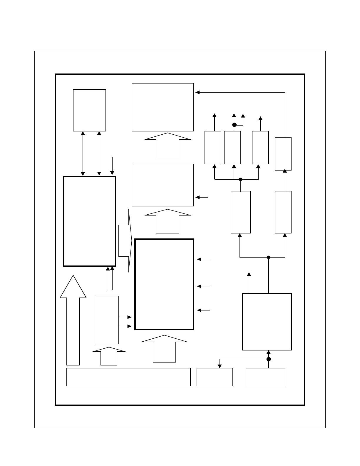
BLOCK DIAGRAM
- 7 -
DC/DC
Converter
(L4973)
12V
ST5V
ST5V
EEPROM
24LC16
ADC/PLL/Scaler
(gmZAN1)
MICOM
(MTV212M)
Switch
FDC6325L
Switch
FDC6325L
Schmitt Trigger
(74HCT14A)
LCD
Interface
20Pin
Connector
(DF14A-20P)
RGB
H.V
D-
Sub
15P
DDC
Control
DC
Jack
SCL
SDA
CON
10P
Inverter
3.3VD
3.3V_PL
Module Power 3.3V
3.3V_PL
3.3VD
ST5V
RGB
3.3V_AD
Regulator
BA033
Regulator
BA033
Regulator
BA033
3.3V_AD
+3.3V
LVDS
(LVDS83)
Regulator
BA033
RIN
RCLK
+3.3V
Hsync2 Vsync2
Hsyncm
Vsyncm
Page 8

DESCRIPTION OF BLOCK DIAGRAM
- 8 -
1. Scaler One chip IC(GMZAN1, U3)
GMZAN1 (U3) is one chip IC which it supports four internal function blocks of Video Amp, PLL, A/D converter and
Video processor.
Video signal (0.7Vp.p) clamped through C44, 45, 191 with matching IC’s proper cut off voltage.
This signal is processed as a proper 8 bit digital signal by U3’s amplifying, phase locking, A/D converting, and scaling
operations.
U3 generates Clock, Horizontal and Vertical sync, Data Enable signals as LCD Panel’s input signals.
2. System Controller (Microprocessor) Circuit
1) Microprocessor (U4) distinguishes polarity and frequency by calculating horizontal and vertical sync input
from signal source.
2) Microprocessor (U4) carries out power control by sending power-down trigger signal to each IC.
3) Microprocessor (U4) communicates with EEPROM (U1), and GMZAN1 (U3)
through IIC(2 lines) or 6 bit bus line. It makes all devices operated properly.
4) Microprocessor (U4) let User adjust screen by OSD function.
3. DC/ DC Converter
This circuit supplies DC power for each device needing DC voltage of 3.3VD, 3.3V_AD, 3.3V_PL, Module Power 3.3V
and 5VS.
L4973D5.1(U13) , the DC/DC controller IC converts input 12Vdc into 5VS and 3.3Vdc with peripheral circuit
composed of Inductor (L11), condensing components (ZD5, C72), and Regulators(U2, U7, U24,U30).
MODPWR(3.3V) for LCD module power is switched by U12, switching FET, controlled by Microprocessor.
3.3VD, 3.3V_AD, and 3.3V_PL for GMZAN1 (U3) and 3.3V for LVDS (U9) are switched by U5, switching FET,
controlled by Microprocessor for Power saving.
4. Display Data Transmitter Part (LVDS).
This part transmit digital signal from the Scaler to the receiver of module.
Page 9
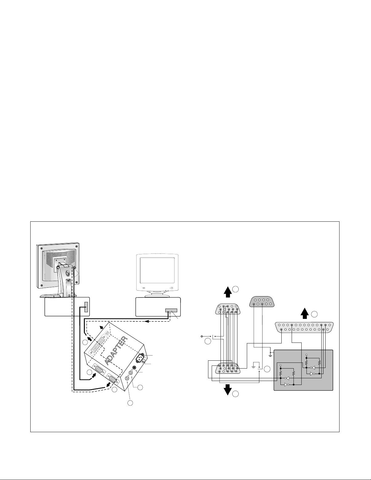
ADJUSTMENT
- 9 -
220
IBM
Compatible PC
PARALLEL PORT
Power inlet (required)
Power LED
ST Switch
Power Select Switch
(110V/220V)
Control Line
Not used
RS232C
PARALLEL
V-SYNC
POWER
ST
VGS
MONITOR
E
E
V-Sync On/Off Switch
(Switch must be ON.)
F
F
A
A
B
B
C
C
15
10
5
5
69
1
1
1
14
13
25
6
5V
5V
5V
4.7K
4.7K
4.7K
74LS06
74LS06
OFF ON
OFF
ON
11
24V
AUDIO
DC OUT
Figure 1. Cable Connection
All adjustment are thoroughly checked and corrected
when the monitor leaves the factory, but sometimes
several minor adjustment may be required.
Adjustment should be following procedure and after
warming up for a minimum of 10 minutes.
Alignment appliances and tools.
- IBM Compatible PC
- Programmable Signal Generator.
(eg. VG-819 made by Astrodesign Co.)
- E(E)PROM with each mode data saved.
- Alignment Adapter and Software.
1. Adjustment for Factory Preset Mode
1) Run alignment program for LB565T on the IBM PC.
2) Select EEPROM ALL Init command and Enter.
3) Display cross hatch pattern at Mode 1.
4) Select FOS DEFAULT command and Enter.
5) Press "Y" key, it will automatically save all FOS data
to EEPROM.
2. Adjustment for White Balance
1) Display color 0,0 pattern at Mode 12.
2) Set External Bright to MAX position and Contrast to
MAX Position.
3) PRESET START command and Enter.
4) BIAS CAL command and Enter.
5) No attempt to manually adjust, BIAS data is automatically adjusted and saved to the EEPROM.
6) Display color 15,0 pattern at Mode 12.
7) Select DRIVE CAL command and Enter.
8) Color 1 (9300K) and Color 2 (6500K) are
automatically adjusted and saved to the EEPROM.
9) Select PRESET EXIT command and Enter.
3. DDC Data Write Procedure
1) Use this procedure only when there is some
probelm on EDID data.
2) Select EEPROM
→ EDID Write command and
Enter.
3) This will write the EDID data to EEPROM.
Page 10

- 10 -
TROUBLESHOOTING GUIDE
1. NO POWER
CHECK U4.
CHECK
U4 PIN 8 VOLTAGE
(5V) ?
NO
NO POWER
(POWER INDICATOR OFF)
CHECK ADAPTER,
AND FIND OUT
A SHORT POINT
AS OPENING
EACH POWER LINE
CHECK J1’S
VOLTAGE
(12V) ?
NO
CHECK L11
(OPEN CHECK)
CHECK
U5 Voltage
(5V) ?
NO
U13’S PIN11
0V ?
CHECK U13, AND
CHECK 5VA LINE
CHECK IIC LINE
CONNECTION
(U4, U1)
CHECK U3’S VCC,
XTAL, RESET
IS U3 PIN12
VOLTAGE REPEATED
AS PULSE SHAPE ?
NO
YES
YES
YES
NO
YES
NO PROBLEM
NO
CHECK KEY CONTROL
CONNECTOR ROUTINE
Page 11

- 11 -
2. NO RASTER (OSD IS NOT DISPLAYED) – INVERTER
CHECK MICOM INV
ON/OFF PORT.
J4 PIN5
5V?
NO
NO RASTER
(OSD IS NOT DISPLAYED)
CHECK ADAPTER
J4 PIN10
12V?
NO
1. CONFIRM BRIGHTNESS
OSD CONTRL STATE.
2. CHECK MICOM DIM-ADJ
PORT
J4 PIN1
5V?
NO
REPLACE
INVERTER ASS’Y
CHECK
PULSE AS
CONTACTING SCOPE
PROBE TO CAUTION LABEL.
(CONTACT PROBE TO
CAUTION LABEL.
CAN YOU SEE PULSE
AT YOUR
SCOPE?
NO
REPLACE CCFL LAMP
IN THE LCD MODULE
YES
YES
YES
YES
Page 12

- 12 -
1. CHECK PIN141, 142
SOLDERING CONDITION
2. CHECK X2
3. TROUBLE IN U3
U3
POWER PINS
3.3V?
NO
CHECK U2, U24
U3 PIN141, 142
OSCILLATE AS 14.3M?
NO
CHECK U5’S SOLDERING
CONDITION AND
CHECK CONNECTION LINE
FROM U3 TO J5
NO
TROUBLE IN CABLE
OR LCD MODULE
CHECK U12, U30
J5 PIN1
3.3V?
NO
YES
YES
YES
YES
3. NO RASTER (OSD IS NOT DISPLAYED) – gmzanl
NO RASTER
(OSD IS NOT DISPLAYED)
J5
PIN2 IS 65MHz CLOCK?
PIN4 IS 48KHz H-SYNC?
PIN5 IS 60Hz V-SYNC?
PIN37 IS 48KHz H-SYNC?
IS PULSE APPEARED
AT SIGNAL PINS?
Page 13

- 13 -
CHECK U2, U24
U3
POWER PIN
3.3V?
NO
1. CHECK PC
2. CHECK SIGNAL CABLE
& D-SUB CONNECTOR
LINE
CHECK
R,G,B INPUT?
U3 PIN 87, 91, 95
NO
CHECK H-SYNC LINE
(D-SUB→U6→MICOM
→U3 PIN150)
CHECK
H-SYNC INPUT
U3 PIN 150?
NO
YES
YES
YES
NO RASTER
(OSD IS DISPLAYED)
4. NO RASTER (OSD IS DISPLAYED) – gmzanl
Page 14

PRINTED CIRCUIT BOARD
- 14 -
C150
C137
C15
1
J5
C112
L301
C301
U30
C152
C151
C129
C134
R81
J1
30
40
C302
C105
20
C111
U12
R79
50
C305 C304
C303
10
U7
C98
C97
D2 C96
U9
C306
DATE :2001.06.21
P/N :6870T375A10-1
1
C110
MODEL:LB565C
D4
D3
L8
C89
L9
C92
R14
C88
C139
C136
C133
C130
80
C90
BA19
70
BA22BA21BA20
60
BA24
L2
50
BA23
L7
R29
D1
R2
J
6
J2
90
C1
R54
R1
C48
40
D6D5
ZD2
ZD1
R28
100
C49
C46
R53
20
30
110
U24
10
C135
C5
120
5
U3
C10
R91
C66
C213
C26
C260
X2
130
U4
140 150
160
U2
C23
U5
C28
R12
RA1RA2
C7
L11
C70
R99
R97
R98
R11
C200
SOLDERING DIRECTION
U8
R15
Q1
R56
C74
U6
R57
R96
R94
R95
C72
X1
C101R72
ZD5
C239
C237
R87
C99
C102
R4
R3
C240
C238
R10
L13
R148
U1
C6
U13
Q3 Q4
L12
J10
C37
1
C38
J4
C236
C235
C230
R86
1. MAIN BOARD (Component Side)
Page 15

- 15 -
2. MAIN BOARD (Solder Side)
R21
R20
C108
C106
R17
R5
R22
C50
R19
R18
R6
C31
C30
C29
C62
C56
C78
C77
C69
C68
C141
C140
R7
C55
C54
C76
C75
C67
C63C79
C80
C61
C35
C85
C84
C45
C33
C138
R44
R43
C36
C47
C43
C32
C42
C191
C73
C44
R42
C60
C231
C232
L1
C18
C3
R41
R40
C51
C39
C34
C132
C16
C2
C52
C82
C81
C53
C83
C22
C11
C13
C24
C27
Q5
ZD4
C91
R34
R37
C12
C19 C17
Q6
R32
R100
R101
R48
R45
R33
C25
R13
R16
R38 C64
C93
R47
R35
C185
C187
C186
C184
C183
C182
C4
Q2
ZD3
C9
R61
R51
C87
C86
R103
R102
L17
L18
L15
C188
R8
D8
R80
R78
R69
R67
R65
R52
R27
R90
R55
R31
R30
R120R82
R74
C20
C8
L14
L16
R184
R60
R73
R70
R49
R26
R23
R25
R24
R9
R75
R64
C65
C59
R149
C155
R147
C40
C41
L23
R68
C57
C58
R150
R183
C156
1
40
5
35
10
30
15
20
25
Page 16

- 16 -
3. CONTROL BOARD (Component Side) 4. CONTROL BOARD (Solder Side)
DATE :2000.05.02
P/N :6870T245C11
1
1
C1
C5
R28
R38
R44
C4
C3
R30
C25
R43
R39
R37
R24
C22
C2C6
R45
R31
R34
C27
R23
P6
Q6
R33
R36
C28
Q4
R26
R29
C24
P4
Q2
R20
R22
C20
P2
Q5
R32
R35
C26
P5
R19
C19
Q1
P1
R21
R25
C23
Q3
P3
R27
Page 17

- 17 -
EXPLODED VIEW
1
2
3
4
7
8
9
10
11
13
12
16
15
5
14
6
Page 18

- 18 -
EXPLODED VIEW PARTS LIST
Ref. No.
1
2
3
4
5
6
7
8
9
10
11
12
13
14
15
16
Part No.
3091TKL028B
6304FTS001A
3809TKL010P
3043TKK057G
4810TKK173A
6631T11012R
6631T11012N
6633TZA003G
6633TZA003F
4951TKS072C
3313TL5035A
4950TKK205C
6871TST244A
6871TST243A
1BWF0302816
332-105G
6634B00046A
6634TBZ016A
6866TD9001G
6866TD9001F
Description
CABINET ASSEMBLY, LB565C BRAND . 575LE 86698 GRAY COLOR, TCO99
LCD(LIQUID CRYSTAL DISPLAY), LTM15C443L TOSHIBA 15.0 INCH XGA(1024 X 768) TFT COLOR W/
BACK COVER ASSY, LB565 3809TKL011 12V (INK)
TILT SWIVEL ASSY, LB575 . STAND(SBHG-1)
BRACKET, LB565C SUPPORTER INVERTER
CONNECTOR ASSEMBLY, 20P H-H 120MM UL20276 PANEL LINK CABLE LM567D
CONNECTOR ASSEMBLY, 20P H-H 120MM UL20276 LM568E INTERFACE,UNIXTAR FOR JAPAN
INVERTER ASSEMBLY, SAMSUNG LG1511 LB565C
INVERTER ASSEMBLY, SAMSUNG LG1509 LB563C FOR JAPAN
METAL ASSEMBLY, FRAME MAIN, LB565C, PEMNUT 4EA
MAIN TOTAL ASSEMBLY, LB565T BRAND CL-18
METAL, REAR LB565
PWB(PCB) ASSEMBLY,SUB, LB565A XAGC BRAND POWER KEY TOTAL
PWB(PCB) ASSEMBLY,SUB, LB565A XAGC BRAND SOFT TOUCH TOTAL
SCREW TAP TITE(B),PAN HEAD WASHER, D3.0 L12.0 MSWR3/(BK)
SCREW, DRAWING, PVS+4*10(MSWR/BK)
ADAPTER, AC-DC, LSE0107A1236 LISHIN 12V 3.0A FOR LG
ADAPTER, AC-DCADP-36UB DELTA 12V 3.0A FOR LG FOR JAPAN
CABLE,D-SUB, UL 2990-9C(7.5) DT 1870MM PANTONE BLUE(661C) LV501A DM
SIGNAL CABLE, UL 2990-9C(7.5) DT 1870MM GRAY(85964) LB500 DM FOR JAPAN
Page 19

- 19 -
DATE: 2002. 4. 29.
*S *AL LOC. NO. PART NO. DESCRIPTION / SPECIFICATION
C1 0CK103CK51A 0.01UF 1608 50V 10% R/TP B(Y5P
C2 0CC221CK41A 220PF 1608 50V 5% R/TP NP0
C3 0CC221CK41A 220PF 1608 50V 5% R/TP NP0
C4 0CK104CK56A 0.1UF 1608 50V 10% R/TP X7R
C5 0CH8107J611 100UF 35V M 85STD(CYL) R/TP
C6 0CK104CK56A 0.1UF 1608 50V 10% R/TP X7R
C8 0CC101CK41A 100PF 1608 50V 5% R/TP NP0
C10 0CH8107F611 100UF 16V M 85STD(CYL) R/TP
C11 0CK104CK56A 0.1UF 1608 50V 10% R/TP X7R
C12 0CK104CK56A 0.1UF 1608 50V 10% R/TP X7R
C13 0CC102CK41A 1000PF 1608 50V 5% R/TP NP0
C15 0CK104CK56A 0.1UF 1608 50V 10% R/TP X7R
C16 0CK104CK56A 0.1UF 1608 50V 10% R/TP X7R
C17 0CC150CK41A 15PF 1608 50V 5% R/TP NP0
C18 0CK104CK56A 0.1UF 1608 50V 10% R/TP X7R
C19 0CC150CK41A 15PF 1608 50V 5% R/TP NP0
C20 0CC101CK41A 100PF 1608 50V 5% R/TP NP0
C22 0CK104CK56A 0.1UF 1608 50V 10% R/TP X7R
C23 0CH8107F611 100UF 16V M 85STD(CYL) R/TP
C24 0CK104CK56A 0.1UF 1608 50V 10% R/TP X7R
C25 0CK104CK56A 0.1UF 1608 50V 10% R/TP X7R
C26 0CH8107F611 100UF 16V M 85STD(CYL) R/TP
C27 0CC102CK41A 1000PF 1608 50V 5% R/TP NP0
C28 0CC102CK41A 1000PF 1608 50V 5% R/TP NP0
C29 0CC330CK41A 33PF 1608 50V 5% R/TP NP0
C30 0CC330CK41A 33PF 1608 50V 5% R/TP NP0
C31 0CC330CK41A 33PF 1608 50V 5% R/TP NP0
C32 0CK104CK56A 0.1UF 1608 50V 10% R/TP X7R
C33 0CK104CK56A 0.1UF 1608 50V 10% R/TP X7R
C34 0CK104CK56A 0.1UF 1608 50V 10% R/TP X7R
C35 0CK104CK56A 0.1UF 1608 50V 10% R/TP X7R
C36 0CK104CK56A 0.1UF 1608 50V 10% R/TP X7R
C37 0CK103CK51A 0.01UF 1608 50V 10% R/TP B(Y5P
C38 0CK103CK51A 0.01UF 1608 50V 10% R/TP B(Y5P
C39 0CK104CK56A 0.1UF 1608 50V 10% R/TP X7R
C40 0CK103CK51A 0.01UF 1608 50V 10% R/TP B(Y5P
C41 0CK103CK51A 0.01UF 1608 50V 10% R/TP B(Y5P
C42 0CK104CK56A 0.1UF 1608 50V 10% R/TP X7R
C43 0CK104CK56A 0.1UF 1608 50V 10% R/TP X7R
C44 0CK103CK51A 0.01UF 1608 50V 10% R/TP B(Y5P
C45 0CK103CK51A 0.01UF 1608 50V 10% R/TP B(Y5P
C46 0CK103CK51A 0.01UF 1608 50V 10% R/TP B(Y5P
C47 0CK104CK56A 0.1UF 1608 50V 10% R/TP X7R
C48 0CH8107F611 100UF 16V M 85STD(CYL) R/TP
C49 0CK103CK51A 0.01UF 1608 50V 10% R/TP B(Y5P
C50 0CC330CK41A 33PF 1608 50V 5% R/TP NP0
C51 0CK104CK56A 0.1UF 1608 50V 10% R/TP X7R
C52 0CK104CK56A 0.1UF 1608 50V 10% R/TP X7R
C53 0CK104CK56A 0.1UF 1608 50V 10% R/TP X7R
C54 0CC330CK41A 33PF 1608 50V 5% R/TP NP0
C55 0CC330CK41A 33PF 1608 50V 5% R/TP NP0
C56 0CC330CK41A 33PF 1608 50V 5% R/TP NP0
C57 0CK104CK56A 0.1UF 1608 50V 10% R/TP X7R
C58 0CC221CK41A 220PF 1608 50V 5% R/TP NP0
C59 0CK104CK56A 0.1UF 1608 50V 10% R/TP X7R
DATE: 2002. 4. 29.
*S *AL LOC. NO. PART NO. DESCRIPTION / SPECIFICATION
C60 0CK104CK56A 0.1UF 1608 50V 10% R/TP X7R
C61 0CK104CK56A 0.1UF 1608 50V 10% R/TP X7R
C62 0CC330CK41A 33PF 1608 50V 5% R/TP NP0
C63 0CC330CK41A 33PF 1608 50V 5% R/TP NP0
C64 0CK104CK56A 0.1UF 1608 50V 10% R/TP X7R
C65 0CK104CK56A 0.1UF 1608 50V 10% R/TP X7R
C66 0CK104CK56A 0.1UF 1608 50V 10% R/TP X7R
C67 0CC330CK41A 33PF 1608 50V 5% R/TP NP0
C68 0CC330CK41A 33PF 1608 50V 5% R/TP NP0
C69 0CC330CK41A 33PF 1608 50V 5% R/TP NP0
C70 0CC101CK41A 100PF 1608 50V 5% R/TP NP0
C72 0CZZTAT002D SVP SANYO 10V 270UF M REEL OSC73 0CC220CK41A 22PF 1608 50V 5% R/TP NP0
C74 0CK104CK56A 0.1UF 1608 50V 10% R/TP X7R
C75 0CC330CK41A 33PF 1608 50V 5% R/TP NP0
C76 0CC330CK41A 33PF 1608 50V 5% R/TP NP0
C77 0CC330CK41A 33PF 1608 50V 5% R/TP NP0
C78 0CC330CK41A 33PF 1608 50V 5% R/TP NP0
C79 0CC330CK41A 33PF 1608 50V 5% R/TP NP0
C80 0CC330CK41A 33PF 1608 50V 5% R/TP NP0
C81 0CK104CK56A 0.1UF 1608 50V 10% R/TP X7R
C82 0CK104CK56A 0.1UF 1608 50V 10% R/TP X7R
C83 0CK104CK56A 0.1UF 1608 50V 10% R/TP X7R
C84 0CC220CK41A 22PF 1608 50V 5% R/TP NP0
C85 0CC220CK41A 22PF 1608 50V 5% R/TP NP0
C86 0CC101CK41A 100PF 1608 50V 5% R/TP NP0
C87 0CC101CK41A 100PF 1608 50V 5% R/TP NP0
C88 0CC680CK41A 68PF 1608 50V 5% R/TP NP0
C89 0CC680CK41A 68PF 1608 50V 5% R/TP NP0
C90 0CC680CK41A 68PF 1608 50V 5% R/TP NP0
C91 0CC680CK41A 68PF 1608 50V 5% R/TP NP0
C92 0CC330CK41A 33PF 1608 50V 5% R/TP NP0
C93 0CK104CK56A 0.1UF 1608 50V 10% R/TP X7R
C96 0CH8107F611 100UF 16V M 85STD(CYL) R/TP
C97 0CK104CK56A 0.1UF 1608 50V 10% R/TP X7R
C98 0CC102CK41A 1000PF 1608 50V 5% R/TP NP0
C99 0CH8227D611 220UF 10V M 85STD (CYL) R/TP
C101 0CC330CK41A 33PF 1608 50V 5% R/TP NP0
C102 0CC330CK41A 33PF 1608 50V 5% R/TP NP0
C105 0CK104CK56A 0.1UF 1608 50V 10% R/TP X7R
C106 0CK104CK56A 0.1UF 1608 50V 10% R/TP X7R
C108 0CK104CK56A 0.1UF 1608 50V 10% R/TP X7R
C110 0CK104CK56A 0.1UF 1608 50V 10% R/TP X7R
C111 0CK104CK56A 0.1UF 1608 50V 10% R/TP X7R
C112 0CH6560K416 56PF 50V J NP0 2012 R/TP
C129 0CC102CK41A 1000PF 1608 50V 5% R/TP NP0
C130 0CC330CK41A 33PF 1608 50V 5% R/TP NP0
C132 0CK104CK56A 0.1UF 1608 50V 10% R/TP X7R
C133 0CC330CK41A 33PF 1608 50V 5% R/TP NP0
C134 0CC102CK41A 1000PF 1608 50V 5% R/TP NP0
C135 0CH8477F611 470UF 16V M 85STD(CYL) R/TP
C136 0CC330CK41A 33PF 1608 50V 5% R/TP NP0
C137 0CH8107F611 100UF 16V M 85STD(CYL) R/TP
C138 0CK104CK56A 0.1UF 1608 50V 10% R/TP X7R
C139 0CC330CK41A 33PF 1608 50V 5% R/TP NP0
C140 0CC330CK41A 33PF 1608 50V 5% R/TP NP0
C141 0CC330CK41A 33PF 1608 50V 5% R/TP NP0
REPLACEMENT PARTS LIST
CAUTION: BEFORE REPLACING ANY OF THESE COMPONENTS,
READ CAREFULLY THE SAFETY PRECAUTIONS IN THIS MANUAL.
* NOTE : S SAFETY Mark
AL ALTERNATIVE PARTS
MAIN BOARD
CAPACITORS
Page 20

DATE: 2002. 4. 29.
*S *AL LOC. NO. PART NO. DESCRIPTION / SPECIFICATION
C150 0CH8107F611 100UF 16V M 85STD(CYL) R/TP
C151 0CK104CK56A 0.1UF 1608 50V 10% R/TP X7R
C152 0CC102CK41A 1000PF 1608 50V 5% R/TP NP0
C155 0CK104CK56A 0.1UF 1608 50V 10% R/TP X7R
C156 0CK104CK56A 0.1UF 1608 50V 10% R/TP X7R
C182 0CK104CK56A 0.1UF 1608 50V 10% R/TP X7R
C183 0CK104CK56A 0.1UF 1608 50V 10% R/TP X7R
C184 0CC330CK41A 33PF 1608 50V 5% R/TP NP0
C185 0CK104CK56A 0.1UF 1608 50V 10% R/TP X7R
C186 0CK104CK56A 0.1UF 1608 50V 10% R/TP X7R
C187 0CK104CK56A 0.1UF 1608 50V 10% R/TP X7R
C188 0CK104CK56A 0.1UF 1608 50V 10% R/TP X7R
C191 0CK103CK51A 0.01UF 1608 50V 10% R/TP B(Y5P
C200 0CK104CK56A 0.1UF 1608 50V 10% R/TP X7R
C213 0CC102CK41A 1000PF 1608 50V 5% R/TP NP0
C230 0CC102CK41A 1000PF 1608 50V 5% R/TP NP0
C231 0CK104CK56A 0.1UF 1608 50V 10% R/TP X7R
C232 0CC102CK41A 1000PF 1608 50V 5% R/TP NP0
C235 0CK104CK56A 0.1UF 1608 50V 10% R/TP X7R
C236 0CK104CK56A 0.1UF 1608 50V 10% R/TP X7R
C237 0CC221CK41A 220PF 1608 50V 5% R/TP NP0
C238 0CK223CK51A 0.022UF 1608 50V 10% R/TP B(Y5
C239 0CH8105K611 1UF 50V M 85STD(CYL) R/TP
C240 0CK104CK56A 0.1UF 1608 50V 10% R/TP X7R
C260 0CK104CK56A 0.1UF 1608 50V 10% R/TP X7R
C301 0CK104CK56A 0.1UF 1608 50V 10% R/TP X7R
C302 0CC150CK41A 15PF 1608 50V 5% R/TP NP0
C303 0CC150CK41A 15PF 1608 50V 5% R/TP NP0
C304 0CC150CK41A 15PF 1608 50V 5% R/TP NP0
C305 0CC150CK41A 15PF 1608 50V 5% R/TP NP0
C306 0CC150CK41A 15PF 1608 50V 5% R/TP NP0
D1 0DS226009AA KDS226 TP KEC SOT-23 80V 300M
D2 0DS226009AA KDS226 TP KEC SOT-23 80V 300M
D3 0DS226009AA KDS226 TP KEC SOT-23 80V 300M
D4 0DS226009AA KDS226 TP KEC SOT-23 80V 300M
D5 0DS226009AA KDS226 TP KEC SOT-23 80V 300M
D6 0DS226009AA KDS226 TP KEC SOT-23 80V 300M
ZD1 0DZ560009DA UDZ S 5.6B TP ROHM-K SOD323 20
ZD2 0DZ560009DA UDZ S 5.6B TP ROHM-K SOD323 20
ZD4 0DZ910009FE UDZS 9.1B TP ROHM - - 9.1V - ZD5 0DR340009AA MBRS340 TP FAIRCHILD NON 40V 3
U1 0ICS240813B CAT24WC08J-TE13 8P,SOIC R/TP 8
U2 0IRH033200A BA033FP-E2 MOLD-3 TP REGULATOR
U3 0IPRPGA001A GMZAN1A-160P GENESIS MICROCHIP
U4 0IZZTSZ159A MYSON DIP 42PIN BK OTP LB565T
U5 0TF632509AA FDC6325L TP FAIRCHILD 8V 2.4A
U6 0IMO741420B MC74HCT14ADR2 14P,SOIC TP LEVE
U7 0IRH033200A BA033FP-E2 MOLD-3 TP REGULATOR
U8 0IKE704200J KIA7042AF SOT-89 TP 4.2V VOLTA
U9 0ITH638300B THC63LVDM83R THINE 56P,TSSOP R
U12 0TF632509AA FDC6325L TP FAIRCHILD 8V 2.4A
U13 0ISG497351A L4973D5.1 SO20 TP 3.5A S/DOWN
U24 0IRH033200A BA033FP-E2 MOLD-3 TP REGULATOR
U30 0IRH033200A BA033FP-E2 MOLD-3 TP REGULATOR
L1 6210TCT002C HF50ACC575018-T TDK ,MM CHIP B
L2 6210TCE001P HB-1S2012-121JT CERATECH 2012M
L7 6210TCE001P HB-1S2012-121JT CERATECH 2012M
DATE: 2002. 4. 29.
*S *AL LOC. NO. PART NO. DESCRIPTION / SPECIFICATION
L8 6210TCE001P HB-1S2012-121JT CERATECH 2012M
L9 6210TCE001P HB-1S2012-121JT CERATECH 2012M
L11 6200TEZ003D TPRH1207-330M BOAM R/TP 33 UH
L12 6210TCE001P HB-1S2012-121JT CERATECH 2012M
L13 6210TCE001P HB-1S2012-121JT CERATECH 2012M
L14 6210TCE001P HB-1S2012-121JT CERATECH 2012M
L15 6210TCE001P HB-1S2012-121JT CERATECH 2012M
L16 6210TCE001P HB-1S2012-121JT CERATECH 2012M
L17 6210TCE001P HB-1S2012-121JT CERATECH 2012M
L18 6210TCE001P HB-1S2012-121JT CERATECH 2012M
L23 6210TCE001S HU-1M2012-121 CERATECH 2012MM
L301 6210TCE001S HU-1M2012-121 CERATECH 2012MM
Q1 0TR390409AE FAIRCHILD KST3904(LGEMTF) TP S
Q3 0TR162309CA KSC1623 TP SAMSUNG SOT23 NPN
Q4 0TR162309CA KSC1623 TP SAMSUNG SOT23 NPN
Q5 0TR390409AE FAIRCHILD KST3904(LGEMTF) TP S
Q6 0TR390409AE FAIRCHILD KST3904(LGEMTF) TP S
R1 0RJ0472D677 47 OHM 1/10 W 5% 1608 R/TP
R2 0RJ4700D677 470 OHM 1/10 W 5% 1608 R/TP
R3 0RJ1500D677 150 OHM 1/10 W 5% 1608 R/TP
R4 0RJ1500D677 150 OHM 1/10 W 5% 1608 R/TP
R5 0RJ0000D677 0 OHM 1/10 W 5% 1608 R/TP
R6 0RJ0000D677 0 OHM 1/10 W 5% 1608 R/TP
R7 0RJ0000D677 0 OHM 1/10 W 5% 1608 R/TP
R9 0RJ1500D677 150 OHM 1/10 W 5% 1608 R/TP
R10 0RJ0000D677 0 OHM 1/10 W 5% 1608 R/TP
R11 0RJ2202D677 22K OHM 1/10 W 5% 1608 R/TP
R12 0RJ1500D677 150 OHM 1/10 W 5% 1608 R/TP
R13 0RJ3301D677 3.3K OHM 1/10 W 5% 1608 R/TP
R14 0RJ0332D677 33 OHM 1/10 W 5% 1608 R/TP
R15 0RJ3301D677 3.3K OHM 1/10 W 5% 1608 R/TP
R16 0RJ4701D677 4.7K OHM 1/10 W 5% 1608 R/TP
R17 0RJ0752D677 75 OHM 1/10 W 5% 1608 R/TP
R18 0RJ0752D677 75 OHM 1/10 W 5% 1608 R/TP
R19 0RJ0752D677 75 OHM 1/10 W 5% 1608 R/TP
R20 0RJ1002D677 10K OHM 1/10 W 5% 1608 R/TP
R21 0RJ0222D677 22 OHM 1/10 W 5% 1608 R/TP
R22 0RJ1000D677 100 OHM 1/10 W 5% 1608 R/TP
R23 0RJ4701D677 4.7K OHM 1/10 W 5% 1608 R/TP
R24 0RJ1002D677 10K OHM 1/10 W 5% 1608 R/TP
R25 0RJ1002D677 10K OHM 1/10 W 5% 1608 R/TP
R26 0RJ4701D677 4.7K OHM 1/10 W 5% 1608 R/TP
R27 0RJ1002D677 10K OHM 1/10 W 5% 1608 R/TP
R28 0RJ4701D677 4.7K OHM 1/10 W 5% 1608 R/TP
R29 0RJ4701D677 4.7K OHM 1/10 W 5% 1608 R/TP
R30 0RJ0332D677 33 OHM 1/10 W 5% 1608 R/TP
R31 0RJ0332D677 33 OHM 1/10 W 5% 1608 R/TP
R32 0RJ2202D677 22K OHM 1/10 W 5% 1608 R/TP
R33 0RJ1000D677 100 OHM 1/10 W 5% 1608 R/TP
R34 0RJ1002D677 10K OHM 1/10 W 5% 1608 R/TP
R35 0RJ4700D677 470 OHM 1/10 W 5% 1608 R/TP
R37 0RJ2701D677 2.7K OHM 1/10 W 5% 1608 R/TP
R38 0RJ1002D677 10K OHM 1/10 W 5% 1608 R/TP
R40 0RJ4701D677 4.7K OHM 1/10 W 5% 1608 R/TP
R41 0RJ4701D677 4.7K OHM 1/10 W 5% 1608 R/TP
R42 0RJ0472D677 47 OHM 1/10 W 5% 1608 R/TP
R43 0RJ0472D677 47 OHM 1/10 W 5% 1608 R/TP
R44 0RJ0472D677 47 OHM 1/10 W 5% 1608 R/TP
R45 0RJ4701D677 4.7K OHM 1/10 W 5% 1608 R/TP
R47 0RJ4701D677 4.7K OHM 1/10 W 5% 1608 R/TP
- 20 -
DIODEs
ICs
COILs & COREs
TRANSISTOR
RESISTORs
Page 21

DATE: 2002. 4. 29.
*S *AL LOC. NO. PART NO. DESCRIPTION / SPECIFICATION
R48 0RJ4701D677 4.7K OHM 1/10 W 5% 1608 R/TP
R49 0RJ4701D677 4.7K OHM 1/10 W 5% 1608 R/TP
R51 0RJ4701D677 4.7K OHM 1/10 W 5% 1608 R/TP
R52 0RJ4701D677 4.7K OHM 1/10 W 5% 1608 R/TP
R53 0RJ0472D677 47 OHM 1/10 W 5% 1608 R/TP
R54 0RJ0472D677 47 OHM 1/10 W 5% 1608 R/TP
R55 0RJ1001D677 1K OHM 1/10 W 5% 1608 R/TP
R60 0RJ1500D677 150 OHM 1/10 W 5% 1608 R/TP
R61 0RJ4701D677 4.7K OHM 1/10 W 5% 1608 R/TP
R64 0RJ1500D677 150 OHM 1/10 W 5% 1608 R/TP
R65 0RJ4701D677 4.7K OHM 1/10 W 5% 1608 R/TP
R67 0RJ4701D677 4.7K OHM 1/10 W 5% 1608 R/TP
R68 0RJ1500D677 150 OHM 1/10 W 5% 1608 R/TP
R69 0RJ4701D677 4.7K OHM 1/10 W 5% 1608 R/TP
R70 0RJ4701D677 4.7K OHM 1/10 W 5% 1608 R/TP
R72 0RJ1004D677 1000000 OHM 1/10 W 5% 1608 R/T
R73 0RJ4701D677 4.7K OHM 1/10 W 5% 1608 R/TP
R74 0RJ4701D677 4.7K OHM 1/10 W 5% 1608 R/TP
R75 0RJ4701D677 4.7K OHM 1/10 W 5% 1608 R/TP
R78 0RJ4701D677 4.7K OHM 1/10 W 5% 1608 R/TP
R79 0RJ2202D677 22K OHM 1/10 W 5% 1608 R/TP
R80 0RJ4701D677 4.7K OHM 1/10 W 5% 1608 R/TP
R81 0RJ1500D677 150 OHM 1/10 W 5% 1608 R/TP
R82 0RJ4701D677 4.7K OHM 1/10 W 5% 1608 R/TP
R86 0RJ3602D677 36K OHM 1/10 W 5% 1608 R/TP
R87 0RJ9101D677 9.1K OHM 1/10 W 5% 1608 R/TP
R90 0RJ1000D677 100 OHM 1/10 W 5% 1608 R/TP
R91 0RJ0000D677 0 OHM 1/10 W 5% 1608 R/TP
R94 0RJ0000D677 0 OHM 1/10 W 5% 1608 R/TP
R96 0RJ1000D677 100 OHM 1/10 W 5% 1608 R/TP
R97 0RJ1000D677 100 OHM 1/10 W 5% 1608 R/TP
R98 0RJ4701D677 4.7K OHM 1/10 W 5% 1608 R/TP
R99 0RJ1000D677 100 OHM 1/10 W 5% 1608 R/TP
RA1 0RHZTCZ001A 100 OHM 1/16 W 5% 3215 R/TP CH
RA2 0RHZTCZ001A 100 OHM 1/16 W 5% 3215 R/TP CH
R100 0RJ1002D677 10K OHM 1/10 W 5% 1608 R/TP
R101 0RJ4701D677 4.7K OHM 1/10 W 5% 1608 R/TP
R102 0RJ4701D677 4.7K OHM 1/10 W 5% 1608 R/TP
R103 0RJ1000D677 100 OHM 1/10 W 5% 1608 R/TP
R120 0RJ1000D677 100 OHM 1/10 W 5% 1608 R/TP
R147 0RJ0472D677 47 OHM 1/10 W 5% 1608 R/TP
R148 0RJ0472D677 47 OHM 1/10 W 5% 1608 R/TP
R149 0RJ1000D677 100 OHM 1/10 W 5% 1608 R/TP
R150 0RJ1000D677 100 OHM 1/10 W 5% 1608 R/TP
J1 6612TAH003A DJ-023 KSD R/ANGLE LB563B
X1 6202TST003D HC-49/SM5H KONY CHIP 12 MHZ 30
X2 6202TST001A SX-1 SUNNY ,SMS, 14.31818MHZ ,
B1 126-005A PKM13EPP-4002-B0 MURATA PIEZO
C19 0CH6050K116 5PF 50V D NP0 2012 R/TP
C20 0CH6050K116 5PF 50V D NP0 2012 R/TP
C21 0CH3104K566 0.1UF 50V K X 2012 R/TP
C22 0CH3104K566 0.1UF 50V K X 2012 R/TP
C23 0CH6050K116 5PF 50V D NP0 2012 R/TP
C24 0CH6050K116 5PF 50V D NP0 2012 R/TP
C25 0CH3104K566 0.1UF 50V K X 2012 R/TP
C26 0CH6050K116 5PF 50V D NP0 2012 R/TP
C27 0CH3104K566 0.1UF 50V K X 2012 R/TP
C28 0CH6050K116 5PF 50V D NP0 2012 R/TP
C30 0CH3104K566 0.1UF 50V K X 2012 R/TP
DATE: 2002. 4. 29.
*S *AL LOC. NO. PART NO. DESCRIPTION / SPECIFICATION
C31 0CH3104K566 0.1UF 50V K X 2012 R/TP
C32 0CH8107F611 100UF 16V M 85STD(CYL) R/TP
C33 0CH3104K566 0.1UF 50V K X 2012 R/TP
C34 0CH3104K566 0.1UF 50V K X 2012 R/TP
C35 0CH3104K566 0.1UF 50V K X 2012 R/TP
C36 0CH3103K516 10000PF 50V K B 2012 R/TP
C37 0CH3103K516 10000PF 50V K B 2012 R/TP
C38 0CH3103K516 10000PF 50V K B 2012 R/TP
C39 DCH7106F621 10UF 16V M 3528MM TP(-)
C42 0CH3104K566 0.1UF 50V K X 2012 R/TP
J10 6602T20008D SMW200-05 YEONHO 2.0MM LOCK S/
J11 6602T20009D SMAW200-05 YEONHO 2.0MM LOCK R
J4 6602T20008H SMW200-09 YEONHO 2.0MM LOCK S/
L1 6210TCT002B ACB2012M-300-T TDK , CHIP BEAD
LD1 0DL305029BA LTL-305DJ-0C2 TP LITEON GREEN/
Q1 0TR390409AE FAIRCHILD KST3904(LGEMTF) TP S
Q10 0TR102009AJ KRC102S NPN SOT-23 TP KEC
Q11 0TR102009AJ KRC102S NPN SOT-23 TP KEC
Q12 0TR102009AJ KRC102S NPN SOT-23 TP KEC
Q13 0TR102009AJ KRC102S NPN SOT-23 TP KEC
Q14 0TR102009AJ KRC102S NPN SOT-23 TP KEC
Q15 0TR102009AJ KRC102S NPN SOT-23 TP KEC
Q16 0TR390409AE FAIRCHILD KST3904(LGEMTF) TP S
Q17 0TR102009AJ KRC102S NPN SOT-23 TP KEC
Q18 0TR390409AE FAIRCHILD KST3904(LGEMTF) TP S
Q19 0TR102009AJ KRC102S NPN SOT-23 TP KEC
Q2 0TR390409AE FAIRCHILD KST3904(LGEMTF) TP S
Q3 0TR390409AE FAIRCHILD KST3904(LGEMTF) TP S
Q4 0TR390409AE FAIRCHILD KST3904(LGEMTF) TP S
Q5 0TR390409AE FAIRCHILD KST3904(LGEMTF) TP S
Q6 0TR390409AE FAIRCHILD KST3904(LGEMTF) TP S
Q8 0TR102009AJ KRC102S NPN SOT-23 TP KEC
Q9 0TR390409AE FAIRCHILD KST3904(LGEMTF) TP S
R1 0RH4701D622 4.7K 1/10W 5 D.R/TP
R19 0RH2402D622 24K OHM 1 / 10 W 2012 5.00% D
R2 0RH1000D622 100 1/10W 5 D.R/TP
R20 0RH2402D622 24K OHM 1 / 10 W 2012 5.00% D
R21 0RH3902D622 39K 1/10W 5 D.R/TP
R22 0RH4702D622 47K 1/10W 5 D.R/TP
R23 0RH1002D622 10K OHM 1 / 10 W 2012 5.00% D
R24 0RH1002D622 10K OHM 1 / 10 W 2012 5.00% D
R25 0RH2402D622 24K OHM 1 / 10 W 2012 5.00% D
R26 0RH2402D622 24K OHM 1 / 10 W 2012 5.00% D
R27 0RH2402D622 24K OHM 1 / 10 W 2012 5.00% D
R28 0RH1001D622 1K OHM 1 / 10 W 2012 5.00% D
R29 0RH3602D622 36K 1/10W 5 D.R/TP
R3 0RH1000D622 100 1/10W 5 D.R/TP
R30 0RH1002D622 10K OHM 1 / 10 W 2012 5.00% D
R31 0RH1002D622 10K OHM 1 / 10 W 2012 5.00% D
R32 0RH2402D622 24K OHM 1 / 10 W 2012 5.00% D
R33 0RH2402D622 24K OHM 1 / 10 W 2012 5.00% D
R34 0RH1001D622 1K OHM 1 / 10 W 2012 5.00% D
R35 0RH3902D622 39K 1/10W 5 D.R/TP
R36 0RH3002D622 30K 1/10W 5 D.R/TP
R37 0RH1002D622 10K OHM 1 / 10 W 2012 5.00% D
R38 0RH1002D622 10K OHM 1 / 10 W 2012 5.00% D
R39 0RH1001D622 1K OHM 1 / 10 W 2012 5.00% D
R41 0RH1001D622 1K OHM 1 / 10 W 2012 5.00% D
R42 0RH1001D622 1K OHM 1 / 10 W 2012 5.00% D
R43 0RH1001D622 1K OHM 1 / 10 W 2012 5.00% D
R44 0RH1001D622 1K OHM 1 / 10 W 2012 5.00% D
R45 0RH1001D622 1K OHM 1 / 10 W 2012 5.00% D
R46 0RH1001D622 1K OHM 1 / 10 W 2012 5.00% D
R47 0RH1001D622 1K OHM 1 / 10 W 2012 5.00% D
R48 0RH1001D622 1K OHM 1 / 10 W 2012 5.00% D
R49 0RH4701D622 4.7K 1/10W 5 D.R/TP
- 21 -
OTHERs
CONTROL BOARD
Page 22

DATE: 2002. 4. 29.
*S *AL LOC. NO. PART NO. DESCRIPTION / SPECIFICATION
R50 0RH1502D622 15K 1/10W 5 D.R/TP
R51 0RH1502D622 15K 1/10W 5 D.R/TP
R52 0RH8200D622 820 1/10W 5 D.R/TP
R53 0RH1501D622 1.5K OHM 1 / 10 W 2012 5.00% D
R54 0RH2201D622 2.2K 1/10W P-TYPE TAPPING
R55 0RH8200D622 820 1/10W 5 D.R/TP
R56 0RH1501D622 1.5K OHM 1 / 10 W 2012 5.00% D
R57 0RH4701D622 4.7K 1/10W 5 D.R/TP
R58 0RH4702D622 47K 1/10W 5 D.R/TP
R59 0RH1000D622 100 1/10W 5 D.R/TP
R61 0RH1501D622 1.5K OHM 1 / 10 W 2012 5.00% D
R62 0RH2200D622 220 1/10W 5 D.R/TP
R63 0RH2200D622 220 1/10W 5 D.R/TP
R66 0RH4700D622 470 1/10W 5 D.R/TP
R67 0RH1000D622 100 1/10W 5 D.R/TP
R73 0RH4701D622 4.7K 1/10W 5 D.R/TP
R74 0RH4700D622 470 1/10W 5 D.R/TP
S10 140-058E SKHV10910B LGEC NON 12V 20A HO
U6 0IPH401300B HEF4013BT 14SOP TP DUAL D FLIP
U7 0IPH401300B HEF4013BT 14SOP TP DUAL D FLIP
U8 0IPH401300B HEF4013BT 14SOP TP DUAL D FLIP
ZD1 0DZ560009DA UDZ S 5.6B TP ROHM-K SOD323 20
ZD2 0DZ560009DA UDZ S 5.6B TP ROHM-K SOD323 20
ZD3 0DZ560009DA UDZ S 5.6B TP ROHM-K SOD323 20
ZD4 0DZ560009DA UDZ S 5.6B TP ROHM-K SOD323 20
ZD5 0DZ560009DA UDZ S 5.6B TP ROHM-K SOD323 20
ZD6 0DZ560009DA UDZ S 5.6B TP ROHM-K SOD323 20
ZD7 0DZ560009DA UDZ S 5.6B TP ROHM-K SOD323 20
ZD8 0DZ560009DA UDZ S 5.6B TP ROHM-K SOD323 20
- 22 -
Page 23

PIN CONFIGURATION
- 25 -
CAT24WC08J-TE13 8P
MC74HCT14ADR2 14P
A
0
A
1
A
2
V
SS
V
CC
WP
SCL
SDA
A
0
A
1
A
2
V
SS
V
CC
WP
SCL
SDA
1
2
3
4
8
7
6
5
1
2
3
4
8
7
6
5
A
0
A
1
A
2
V
SS
V
CC
WP
SCL
SDA
1
2
3
4
8
7
6
5
PIN CONFIGURATION
DIP Package(p) SOIX Package(J)
TSSOP Package(U)
BLOCK DIAGRAM
PIN FUNCTION
Pin Name
A0, A1, A2
SDA
SCL
WP
Vcc
Vss
Function
Device Adress Inputs
Serial Data/Address
Serial Clock
Write Protect
+1.8V to + 6.0V power Supply
Ground
V
A1
Y1
AS
A2
Y6
Y2
A5
A3
Y5
Y3
A4
GND
Y4
CC
1
2
3
4
5
6
7
14
13
12
11
10
9
8
PIN CONFIGURATION
BLOCK DIAGRAM
EXTERNAL LOAD
V
V
SDA
WP
SCL
CC
SS
D
OUT
ACK
WORD ADDRESS
BUFFERS
START/STOP
LOGIC
XDEC
CONTROL
LOGIC
STATE COUNTERS
A
0
A
1
A
2
SLAVE
ADDRESS
COMPARATORS
SENSE AMPS
SHIFT REGISTERS
COLUMN
DECODERS
2
E PROM
DATA IN STORAGE
HIGH VOLTAGE/
TIMING CONTROL
12
A1 Y1
34
A2 Y2
56
A3 Y3
98
A4 Y4
11 10
A5 Y5
13 12
A6
PIN 14=V
CC
PIN 7=GND
Y6
Page 24

SCHEMATIC DIAGRAM
- 24 -
1. GMZAN1
Page 25

- 25 -
2. LVDS
Page 26

- 26 -
3. MICOM
Page 27

- 27 -
4. POWER
Page 28

- 28 -
5. CONNECTOR & JACKS
Page 29

- 29 -
6. KEY CONTROL
Page 30

Apr. 2002
P/NO : 3828TSL072L Printed in Korea
 Loading...