

CAR CD/MP3/WMA
RECEIVER
SERVICE MANUAL
CAUTION
BEFORE SERVICING THE UNIT, READ THE “SAFETY PRECAUTIONS”
IN THIS MANUAL.
P/N : AFN31552406 AUGUST, 2006
MODEL:LAC-M5600/LAC-UA560
SERVICE MANUAL MODEL:LAC-M5600/LAC-UA560

- 1-1 -
[CONTENTS]
❍ SECTION 1.GENERAL
• SERVICING PRECAUTIONS . . . . . . . . . . . . . . . . . . . . . . . . . . . . . . . . . . . . . . . . . . . . . . . 1-2
• ESD PRECAUTIONS . . . . . . . . . . . . . . . . . . . . . . . . . . . . . . . . . . . . . . . . . . . . . . . . . . . . . 1-3
• SPECIFICATIONS . . . . . . . . . . . . . . . . . . . . . . . . . . . . . . . . . . . . . . . . . . . . . . . . . . . . . . . .1-4
• LOCATION OF CUSTOMER CONTROLS . . . . . . . . . . . . . . . . . . . . . . . . . . . . . . . . . . . . . . .1-5
• INSTALLATION . . . . . . . . . . . . . . . . . . . . . . . . . . . . . . . . . . . . . . . . . . . . . . . . . . . . . . . . . . .1-7
• CONNECTION DIAGRAM . . . . . . . . . . . . . . . . . . . . . . . . . . . . . . . . . . . . . . . . . . . . . . . . . . .1-8
❍ SECTION 2. ELECTRICAL
• ELECTRICAL TROUBLESHOOTING GUIDE . . . . . . . . . . . . . . . . . . . . . . . . . . . . . . . . . . . . 2-1
• WAVEFORMS OF MAJOR CHECK POINT . . . . . . . . . . . . . . . . . . . . . . . . . . . . . . . . . . . . . 2-6
• INTERNAL BLOCK DIAGRAM of ICs . . . . . . . . . . . . . . . . . . . . . . . . . . . . . . . . . . . . . . . . . 2-7
• BLOCK DIAGRAM (WHOLE) . . . . . . . . . . . . . . . . . . . . . . . . . . . . . . . . . . . . . . . . . . . . . . . 2-21
• BLOCK DIAGRAM (CDP) . . . . . . . . . . . . . . . . . . . . . . . . . . . . . . . . . . . . . . . . . . . . . . . . . .2-23
• SCHEMATIC DIAGRAMS . . . . . . . . . . . . . . . . . . . . . . . . . . . . . . . . . . . . . . . . . . . . . . . . . 2-25
• PRINTED CIRCUIT DIARGAMS . . . . . . . . . . . . . . . . . . . . . . . . . . . . . . . . . . . . . . . . . . . . 2-35
❍ SECTION 3. EXPLODED VIEWS
• CABINET AND MAIN FRAME SECTION . . . . . . . . . . . . . . . . . . . . . . . . . . . . . . . . . . . . . . . 3-1
- ACCESSORY . . . . . . . . . . . . . . . . . . . . . . . . . . . . . . . . . . . . . . . . . . . . . . . . . . . . . . . . . . .3-2
• MECHANISM (PICK-UP) . . . . . . . . . . . . . . . . . . . . . . . . . . . . . . . . . . . . . . . . . . . . . . . . . . . 3-3
❍ SECTION 4. REPLACEMENT PARTS LIST . . . . . . . . . . . . . . . . . . . . . . . . . . .4-1

- 1-2 -
❏ SERVICING PRECAUTIONS
❶ Always disconnect the power source before:
1) Removing or reinstalling any component, circuit board, module or any other instrument assembly.
2) Disconnecting or reconnecting any instrument electrical plug or other electrical connection.
3) Connecting a test substitute in parallel with an electrolytic capacitor in the instrument.
CAUTION: A wrong part substitution or incorrect polarity installation of electrolytic capacitors may result in
an explosion hazard.
❷ Do not defeat any plug/socket B+ voltage interlocks with which instruments covered by
this service manual might be equipped.
❹ Do not apply power to this instrument and or any of its electrical assemblies unless all
solid-state device heat sinks are correctly installed.
❸ Always connect a test instrument’s ground lead to the instrument chassis ground before
connecting the test instrument positive lead. Always remove the test instrument ground
lead last.
1) The service precautions are indicated or printed on the cabinet, chassis or components. When servicing,
follow the printed or indicated service precautions and service materials.
2) The Components used in the unit have a specified conflammability and dielectric strength. When replacing any components, use components which have the same ratings. Components marked in the circuit diagram are important for safety or for the characteristics of the unit. Always replace with the exact
components.
3) An insulation tube or tape is sometimes used and some components are raised above the printed writing
board for safety. The internal wiring is sometimes clamped to prevent contact with heating components.
Install them as they were.
4) After servicing always check that the removed screws, components and wiring have been installed correctly and that the portion around the service part has not been damaged. Further check the insulation
between the blades of attachment plug and accessible conductive parts.
SECTION 1. SUMMARY
- 1-3 -
❏ ESD PRECAUTIONS
Electrostatically Sensitive Devices (ESD)
Some semiconductor (solid state) devices can be damaged easily by static electricity. Such components
commonly are called Electrostatically Sensitive Devices (ESD). Examples of typical ESD devices are integrated
circuits and some field-effect transistors and semiconductor chip components.The following techniques should
be used to help reduce the incidence of component damage caused by static electricity.
1. Immediately before handling any semiconductor component or semiconductor-equipped assembly, drain off
any electrostatic charge on your body by touching a known earth ground. Alternatively, obtain and wear a
commercially available discharging wrist strap device, which should be removed for potential shock reasons
prior to applying power to the unit under test.
2. After removing an electrical assembly equipped with ESD devices, place the assembly on a conductive surface such as aluminum foil, to prevent electrostatic charge buildup or exposure of the assembly.
3. Use only a grounded-tip soldering iron to solder or unsolder ESD devices.
4. Use only an anti-static solder removal device. Some solder removal devices not classified as "anti-static" can
generate electrical charges sufficient to damage ESD devices.
5. Do not use freon-propelled chemicals. These can generate electrical charges sufficient to damage ESD
devices.
6. Do not remove a replacement ESD device from its protective package until immediately before you are
ready to install it. (Most replacement ESD devices are packaged with leads electrically shorted together by
conductive foam, aluminum foil or comparable conductive materials).
7. Immediately before removing the protective material from the leads of a replacement ESD device, touch the
protective material to the chassis or circuit assembly into which the device will by installed.
CAUTION : BE SURE NO POWER IS APPLIED TO THE CHASSIS OR CIRCUIT, AND OBSERVE ALL
OTHER SAFETY PRECAUTIONS.
8. Minimize bodily motions when handing unpackaged replacement ESD devices. (Otherwise harmless motion
such as the brushing together of your clothes fabric or the lifting of your foot from a carpeted floor can generate static electricity sufficient to damage an ESD device).
CAUTION. GRAPHIC SYMBOLS
THE LIGHTNING FLASH WITH APROWHEAD SYMBOL. WITHIN AN EQUILATERAL TRIANGLE,
IS INTENDED TO ALERT THE SERVICE PERSONNEL TO THE PRESENCE OF UNINSULATED
“DANGEROUS VOLTAGE” THAT MAY BE OF SUFFICIENT MAGNITUDE TO CONSTITUTE A
RISK OF ELECTRIC SHOCK.
THE EXCLAMATION POINT WITHIN AN EQUILATERAL TRIANGLE IS INTENDED TO ALERT
THE SERVICE PERSONNEL TO THE PRESENCE OF IMPORTANT SAFETY INFORMATION IN
SERVICE LITERATURE.

- 1-4 -
❏ SPECIFICATIONS
MP3/WMA Disc compatibility with this unit is limited as follows:
1. Sampling Frequency / 8 - 48kHz (MP3) 22.05 - 48kHz (WMA)
2. Bit rate / within 8 - 320kbps (include VBR) (MP3) 32 -320kbps (WMA)
3. CD-R/CD-RW physical format should be “ISO 9660”
4. If you record MP3/WMA files using software which cannot create a FILE SYSTEM, for example
“Direct-CD” etc., it will not be possible to playback MP3/WMA files. We recommend that you use
“Easy-CD Creator” which can create an ISO9660 file system.
Customers should also note that permission is required in order to download MP3/WMA files and
music from the Internet.
Our company has no right to grant such permission.
Permission should always be sought from the copyright owner.
GENERAL
Output Power . . . . . . . . . . . . . . . . . . . . . . . . . . . . . . . . . . . . . . . . . . . . . .50W x 4CH (Max.)
Power Source . . . . . . . . . . . . . . . . . . . . . . . . . . . . . . . . . . . . . . . . . . . . . . . . . . . . . .DC 12V
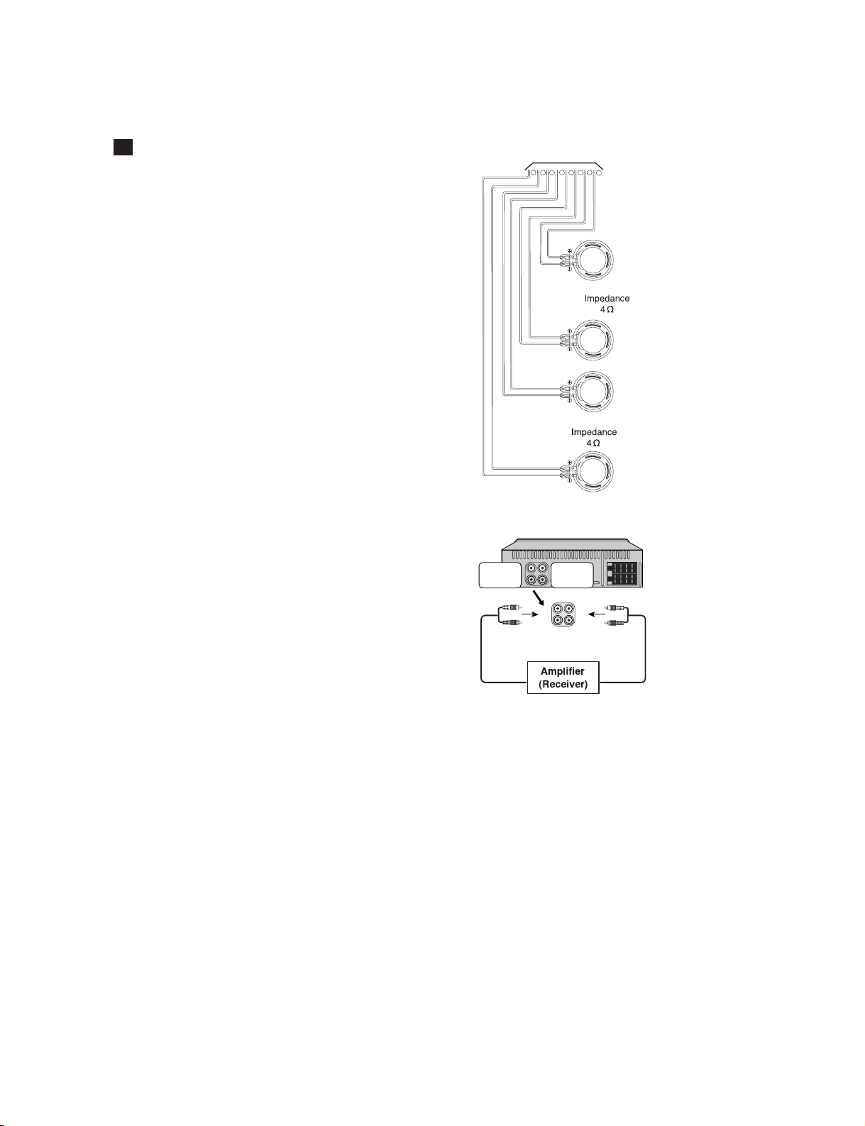
Speaker impedance . . . . . . . . . . . . . . . . . . . . . . . . . . . . . . . . . . . . . . . . . . . . . . . . . . . . .4 Ω
Ground System . . . . . . . . . . . . . . . . . . . . . . . . . . . . . . . . . . . . . . . . . . . . . . . . . . . . Negative
Dimensions (W x H x D) . . . . . . . . . . . . . . . . . . . . . . . .180 x 51 x 171 mm (Without Front Panel)
Net Weight . . . . . . . . . . . . . . . . . . . . . . . . . . . . . . . . . . . . . . . . . . . . . . . . . . . . . . . . . .1.4 kg
CD SELECTION
Frequency Response . . . . . . . . . . . . . . . . . . . . . . . . . . . . . . . . . . . . . . . . . . . .20 Hz-20 kHz
S/N Ratio . . . . . . . . . . . . . . . . . . . . . . . . . . . . . . . . . . . . . . . . . . . . . . . . . . . . . . . . . . .80 dB
Distortion . . . . . . . . . . . . . . . . . . . . . . . . . . . . . . . . . . . . . . . . . . . . . . . . . . . . . . . . . . . .0.1%
Channel Separation (1kHz) . . . . . . . . . . . . . . . . . . . . . . . . . . . . . . . . . . . . . . . . . . . . .70 dB
RADIO SELECTION
FM
Frequency Range . . . . . . . . . . . . . . . . . . . . . . . . . . . . . .65-74, 87.5-107.9 or 87.5-108 MHz
S/N Ratio . . . . . . . . . . . . . . . . . . . . . . . . . . . . . . . . . . . . . . . . . . . . . . . . . . . . . . . . . . .55 dB
Distortion . . . . . . . . . . . . . . . . . . . . . . . . . . . . . . . . . . . . . . . . . . . . . . . . . . . . . . . . . . .0.7%
Usable Sensitivity . . . . . . . . . . . . . . . . . . . . . . . . . . . . . . . . . . . . . . . . . . . . . . . . . .12 dBµV
AM (MW)
Frequency Range . . . . . . . . . . . . . . . . . . . . . . . . . . . . . . . . . . . . .520-1720 or 522-1620 kHz
S/N Ratio . . . . . . . . . . . . . . . . . . . . . . . . . . . . . . . . . . . . . . . . . . . . . . . . . . . . . . . . . . .45 dB
Distortion . . . . . . . . . . . . . . . . . . . . . . . . . . . . . . . . . . . . . . . . . . . . . . . . . . . . . . . . . . . .1.0%
Usable Sensitivity . . . . . . . . . . . . . . . . . . . . . . . . . . . . . . . . . . . . . . . . . . . . . . . . . .28 dBµV
- 1-5 -
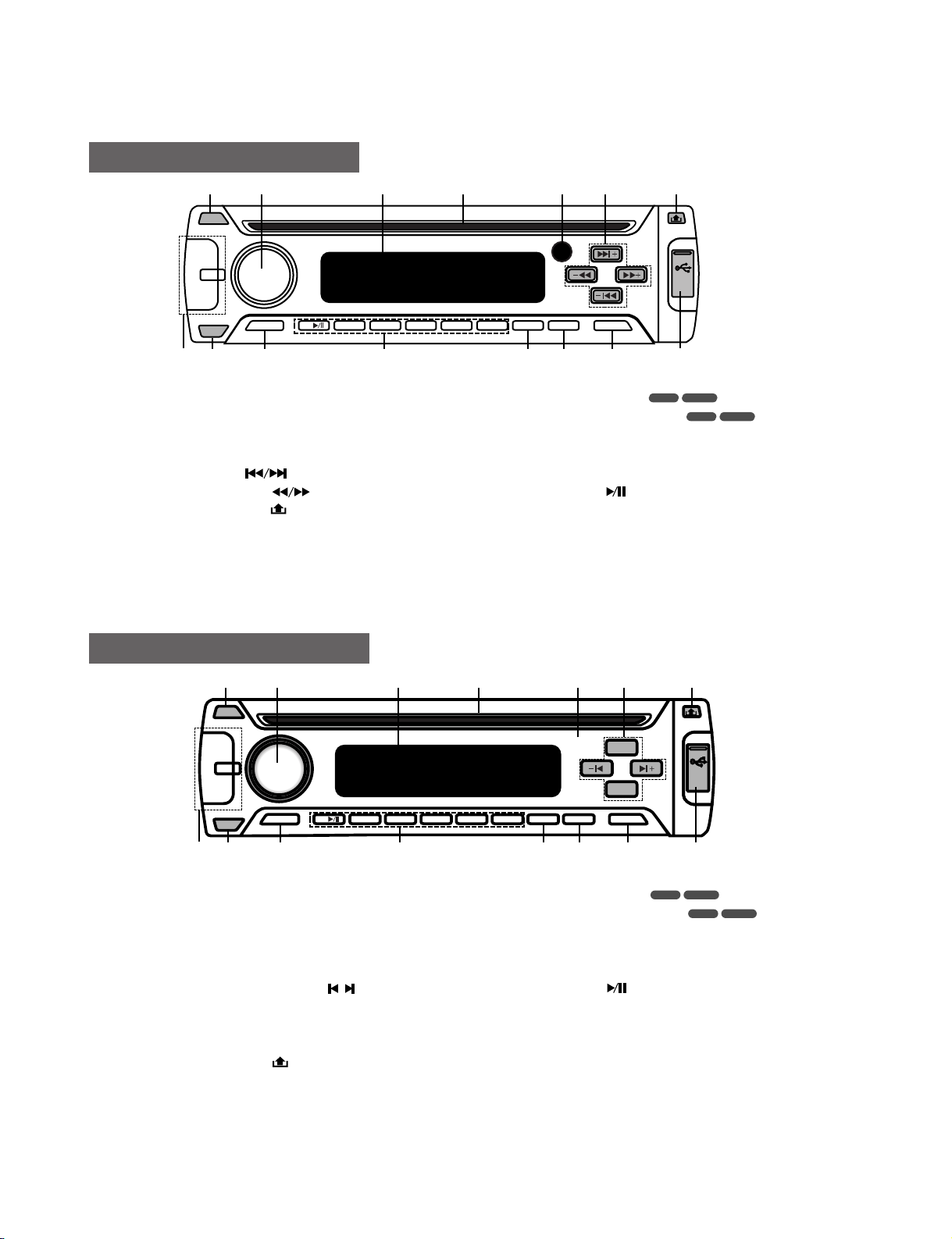
❏ LOCATION OF CUSTOMER CONTROLS
12 3 6 7
8
5
1314 12 10 9
4
15
1[EJECT]
2 POWER / VOLUME [PWR/VOL]
3 DISPLAY WINDOW
4 DISC SLOT
5 REMOTE SENSOR
6 • SKIP / SEEK
• SEARCH / TUNE -/+
7 RELEASE
8 USB Port [USB]
9 DISPLAY / CLOCK [DISP / CLK]
10 EQUALIZER [EQ]
11 • AUTO STORE [AS]
• PRESET SCAN [PS]
12 • PRESET STATION [1-6]
• MP3 TRACK +10/-10
• FOLDER UP/DOWN [F+/F-]
• SHUFFLE [SHF]
• REPEAT [RPT]
• INTRO SCAN [SCAN]
• PLAY/PAUSE
13 Extreme Dynamic Sound System [XDSS]
14 SOURCE [SRC]
15 • [MUTE]
• SELECT [SEL]
• [BAND]
WMAMP3
WMAMP3
11
1[EJECT]
2 •
POWER [PWR]
• VOLUME/MUTE [VOL / MUTE]
3 DISPLAY WINDOW
4 DISC SLOT
5 REMOTE SENSOR
6 • CD SKIP/SEARCH /
• SEEK / TUNE -/+
• PROGRAM TYPE [PTY]
• TRAFFIC ANNOUNCEMENT [TA]
7 RELEASE
8 USB Port [USB]
9 DISPLAY / CLOCK [DISP / CLK]
10 EQUALIZER [EQ]
11 • AUTO STORE [AS]
• PRESET SCAN [PS]
12 • PRESET STATION [1-6]
• MP3 TRACK +10/-10
• FOLDER UP/DOWN [F+/F-]
• SHUFFLE [SHF]
• REPEAT [RPT]
• INTRO SCAN [SCAN]
• PLAY/PAUSE
13 Extreme Dynamic Sound System [XDSS]
14 SOURCE [SRC]
15 • ALTERNATIVE FREQUENCIES [AF]
• REGIONAL [REG]
• SELECT [SEL]
• [BAND]
WMAMP3
WMAMP3
AF/REG
EJECT
SRC
BAND
SEL
PWR
XDSS
VOL/MUTE
1
SC
AN
2
RPT
3
SHF
4
F-5F
+
6
AS/PS EQ
TA
PTY
DISP/CLK
USB
12 3 6 7
8
5
1314 12 10 9
4
15
11
1. Front Panel (LAC-M5600)
2. Front Panel (LAC-M5600R)
EJECT
MUTE
BAND
SEL
SRC
PWR
VOL
XDSS
2
1
SCAN
4
3
SHF
RPT
F-
5F+6
AS/PS EQ
DISP/CLK
USB
- 1-6 -
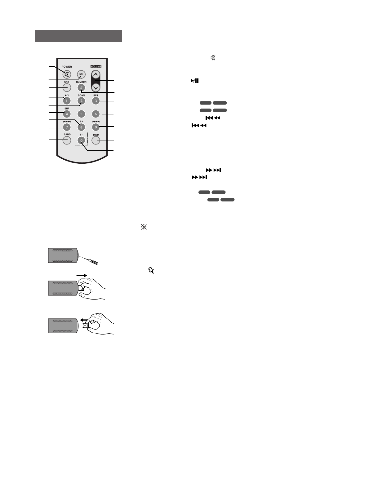
1 Remove the battery holder with a pencil or ball point pen.
2 Install the battery on the battery holder.
3 Install the battery holder back into its original position.
Notes
• Use only one CR2025 (3V) lithium battery.
• Remove the battery if the remote control is not used for a
long period of time.
• Do not leave the product in a hot or humid place.
• Do not handle the battery using metallic tools.
• Do not store the battery together with metallic materials.
• In the event of battery leakage, wipe the remote control
completely clean and install a new battery.
Battery installation
Remote Control
10
12
14
15
16
1
3
8
9
4
5
2
6
7
11
13
1 POWER [PWR] / MUTE
2 SELECTION [SEL]
3 SOURCE [SRC]
4 PLAY / PAUSE
5 INTRO SCAN [SCAN]
6 SHUFFLE [SHF]
7 • MP3 TRACK +10
• FOLDER UP [F+]
8 • CD SKIP / SEARCH
• SEEK / TUNE
9[BAND]
10 VOLUME UP
<
<
/ DOWN
11 NUMBER [#]
12 REPEAT [RPT]
13 NUMBER [0 -9]
14 • CD SKIP / SEARCH
• SEEK / TUNE
15 DISPLAY [DISP.]
16 • MP3 TRACK -10
• FOLDER DOWN [F-]
WMAMP3
WMAMP3
WMAMP3
WMAMP3
3. Remote control
- 1-7 -
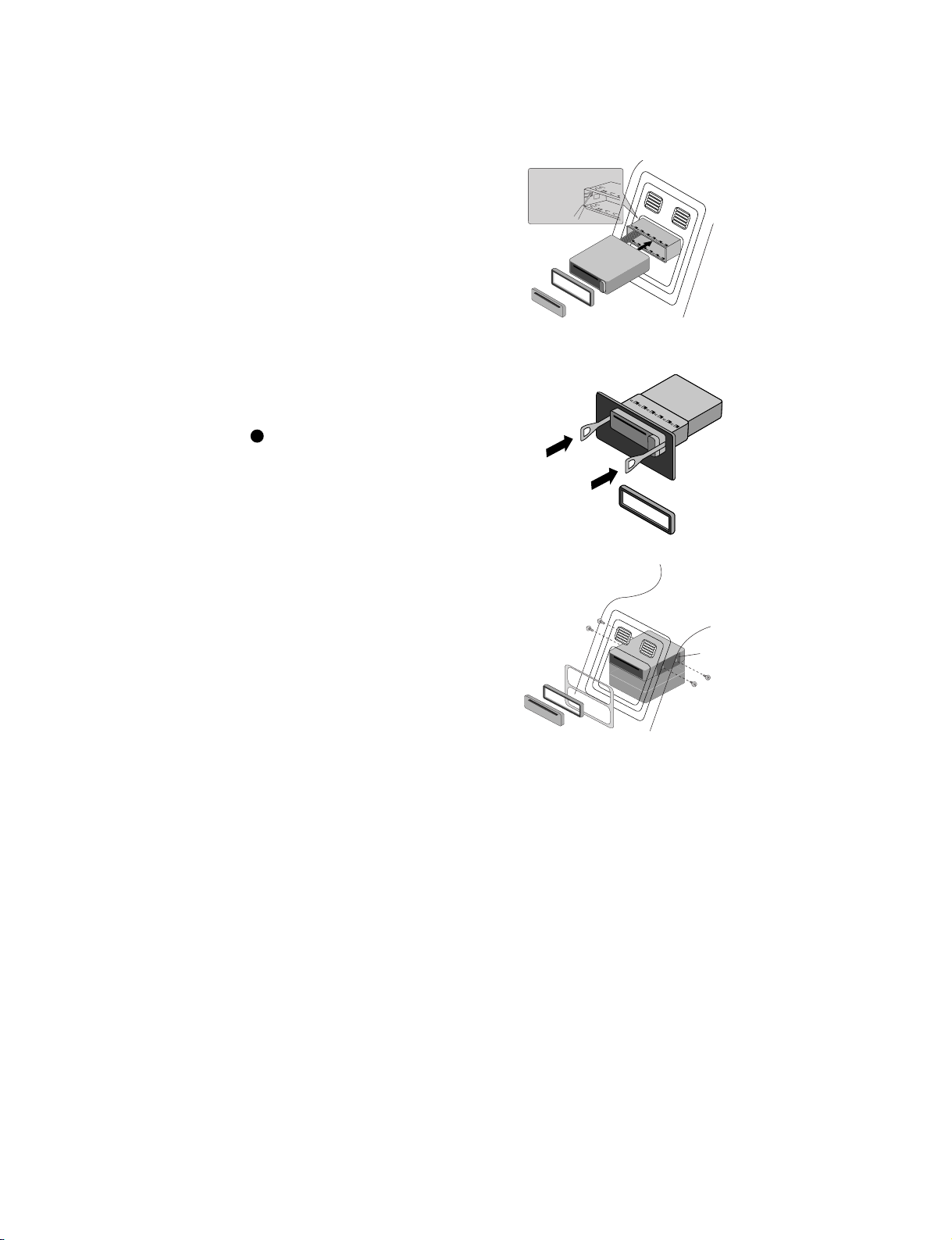
❏ INSTALLATION
5
4
3
1
2
6
Front panel
Before installing, make sure that the ignition switch is set to
OFF and remove the terminal of the car battery to avoid
short-circuiting.
1 Remove the existing receiver unit.
2 Make the necessary connections.
3 Install the installation sleeve.
4 Install the unit into the installation sleeve.
Removing the existing receiver unit.
Please remove any installation sleeves already in place for the
receiver unit in the dashboard, it must be removed.
1 Remove the rear support from the unit.
2 Remove the front panel and trim ring from the unit.
3 Insert the lever into the hole on one side of the unit.
Perform the same operation on the other side and pull the
unit out from the mounting sleeve.
Basic Installation
1 Slide the unit into the ISO-DIN frame.
2 Install the screws removed from the old unit.
3 Slide the unit and frame into the dash opening.
4 Install the dash panel or adapter plate.
5 Install the trim ring into unit.
6 Install the faceplate by fitting the right edge into position
then pushing the left edge closed.
ISO-DIN Installation
Bend the claws
according to
the thickness
of the
dashboard
Front panel
A
A
•
•
A
- 1-8 -
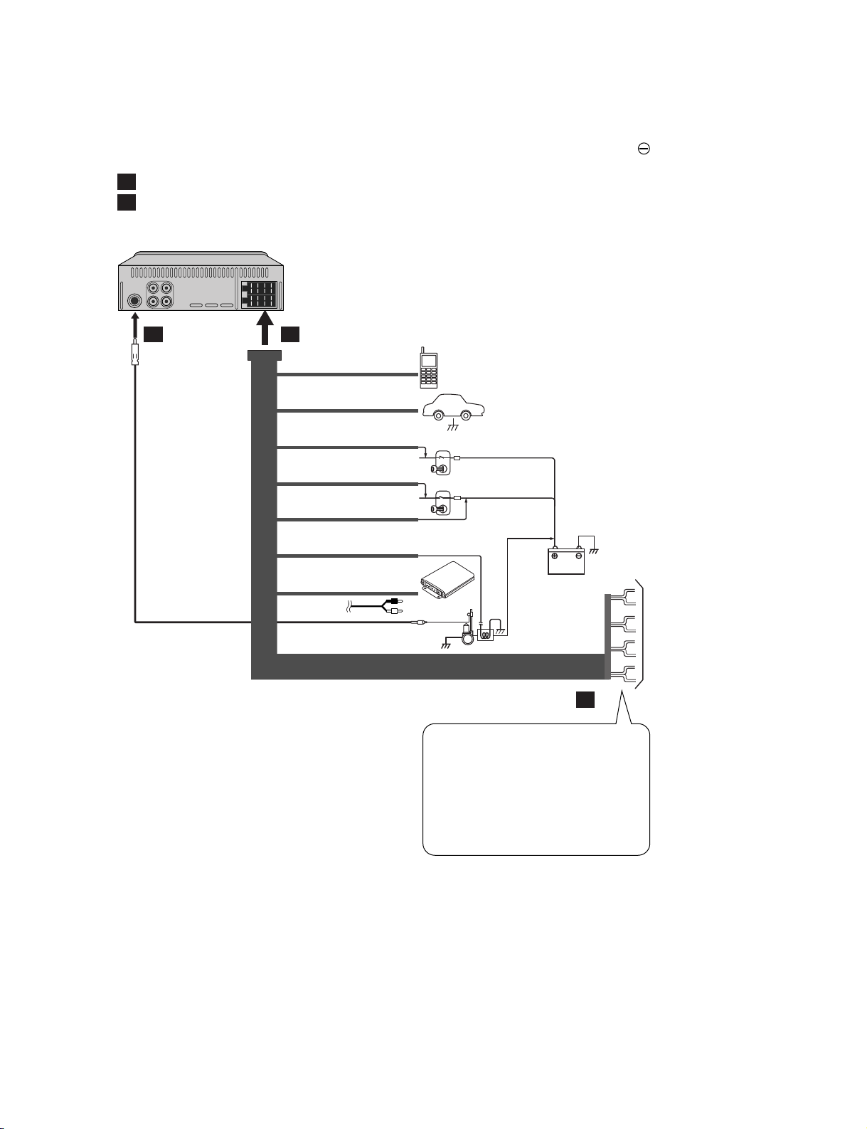
❏ CONNECTION DIAGRAM
Before connecting, make sure that the ignition switch is set to OFF, and remove the battery
terminal to avoid short circuits.
1
2
3
4
5
6
7
8
BATTERY
POWER
ANT
DIMMER SWITCH
IGNITION SWITCH
CONTROL RELAY
REMOTE ON (BLUE/WHITE)
AMPLLIFIER
(Optional)
PHONE MUTE (ORANGE)
DIMMER (PINK)
TO IGNITION (RED)
GROUND(-) (BLACK)
POWER ANTENNA (BLUE)
TO BATTERY(+) (YELLOW)
1. WHITE FL+
2. WHITE/BLACK STRIPE FL-
3. GRAY FR+
4. GRAY/ BLACK STRIPE FR-
5. GREEN RL+
6. GREEN/ BLACK STRIPE RL-
7. VIOLET RR+
8. VIOLET/ BLACK STRIPE RR-
From antenna
To the wiring of the vehicle colors of leads.
A
B
A B
C
- 1-9 -
• BLACK : This lead is for the ground connection.
• ORANGE : This lead is for the phone line connection.
• PINK : This lead is for the dimmer line
connection.
• RED : This lead is for connection to the power
supply terminal when the ignition switch is
set to ACC.
• YELLOW : This lead is for connection to the battery
(back-up) terminal from which power is
always supplied.
• BLUE : This lead is for the power antenna
connection.
• BLUE/WHITE : This lead is for the remote amplifier on
connection.
L
R
L
R
1
2345678
REAR
FRONT
Connect the AUDIO OUTPUT connector of this unit to the
AUDIO INPUT connector of the Auxiliary Equipment.
Connecting to Auxiliary Equipment (Optional)
To AUDIO IN
To AUDIO IN
To AUDIO OUT
FL (Front Left)
FR (Front Right)
RL (Rear Left)
RR (Rear Right)
Speaker Connections
C

- 1-10 -
- 2-1 -
❏ ELECTRICAL TROUBLESHOOTING GUIDE
1. No Power.
Any Key power on.
YES
YES
YES
YES
YES
YES
NO
NO
NO
NO
NO
Is power turnd on?
DISC loading?
Does initial reading occur?
Can disc be played?
Is audio output supplied?
OK
Check audio circuitry.
IC506, PN502
Check tracking servo circuitry.
Q501, IC506, IC504
Check DISC.
Check focusing circuitry.
Q501, IC506
Check laser circuitry.
Q501, IC506
Check loading supply circuitry.
IC802 Pin .
Check power supply circuitry.
IC802 Pin .
SECTION 2. ELECTRICAL
6
14
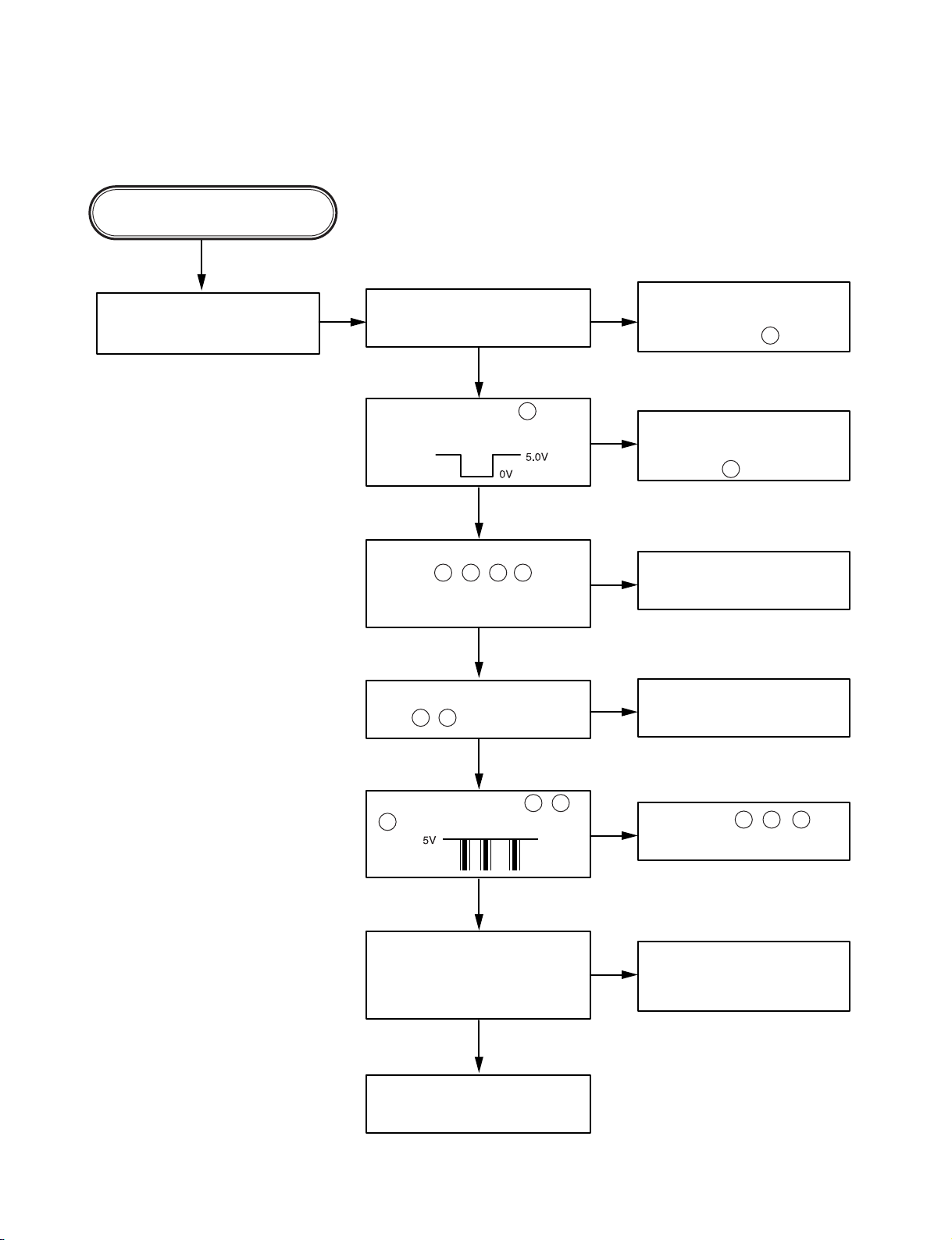
- 2-2 -
2. LCD light abnornal.
YES
YES
YES
YES
YES
YES
NO NO
NO
NO
NO
NO
NO
Any Key power on.
(without DISC)
Do display LCD then light?
Check voltage in the power
supply circuitry.
Power supply circuitry defective.
• Check Q403, Q404, Q406,
Q407, IC802 Pin .
• Reset circuit defective.
IC901 Surrounding circuit
defective.
• IC901 Pin defective.
Check X401, X402, C402,
C403, C404, C505.
PN401 or PN903 or front
PCB pattern defective.
IC401, Pins , , or
front PCB pattern defective.
IC901 Surrounding circuit
PCB pattern defective.
Display LCD connector
defective.
Is IC901 Com1, Com2, Com3
output waveform normal?
Is u-com IC401 Pins , ,
output waveform normal?
Is u-com IC401 pin reset
circuit normal?
Is u-com IC401 keyin
Pins , 5volt input?
Is u-com IC401 X1, X2 terminal Pins , , , input?
OSC : 19.2MHz
OSC : 32.768kHz
4
74
57
11
63
74 75 76
74 75
76
64
12 14 15

- 2-3 -
3. Initial reading is not carried out.
YES
YES
YES
YES
YES
YES
YES
YES
YES
YES
YES
YES
YES (with disc)
NO NO
NO
NO
NO
NO
NO
NO
NO
NO
NO
Slide motor moves.
(With disc)
Spindle motor turns.
(Refer to FIG3.)
Does RF waveform
appear at IC506 Pin
(Refer to FIG4.)
Check the Voltage change of
PN502 Pin (6.4~6.8V).
Check the Voltage change of PN506
Pins , , , . (1.4V~1.8V).
Check the Data transmission
from IC510 pins , ,
(Refer to FIG7.)
Check the Data transmission
from IC510 pins , ,
(Refer to FIG8.)
Check the TRVP
Voltage.
(IC506 Pins )
Check the change of
SL +, SL – Voltage.
(IC504 Pins , )
Does FA+ waveform appear
at IC504 Pin ?
(Refer to FIG1.)
Laser light check A ?
Defective contact
PN501 or PICK-UP
Defective IC504
Defective IC506
Defective IC506
Defective MICOM
Defective IC506
Defective
Connector. (PN502)
Does TE waveform appear at
R517? (Refer to FIG2.)
Is rotation normal?
Is there no dropout of RF signal?
Defective IC506 or
PICK-UP
1
42
26 76 7742
58
48
23
13
15
14
57 71
70 72

- 2-4 -
When laser does not light.
A
Is “2.4V~3.4V” applied to
pin42 of IC506?
( ➀ 3.4V ➁ 2.4V)
Did pickup return to
innermost circular?
Does it stop at inner pick
circular after shift?
Is defect output from LMT
SW applied to 68 of IC510?
Is data transferred
from IC510?
Does voltage appear at
IC504 Pins , ?
Defective MICOM (IC510)
Defective IC504
Defective slide motor
and/or connector(PN504)
Defective LMT SW and/or
connector(PN504)
Defective MICOM(IC510)
Defective IC506
Is power supplied to laser Q501?
(Q501 collector: about 1.8V)
OV
YES
YES
YES
YES
YES
YES
NO
NO
NO
NO
NO
NO
OPEN CLOSE
13 14

- 2-5 -
NO
YES
YES
4. USB awareness badness (Refer to FIG5, 6.)
USB connection
• Check power supply.
(IC301, IC302, PN301, CN702, CN703)
• Check USB memory.
• Check USB Circuit.
(IC509, IC511, CN701, CN702, PN503)
Normalcy operation
OK
When laser light.
B
When SPINDLE motor dose not turn
C
NO
NO
NO
NO
YES
YES
YES
YES
Laser lights?
Check the signal FOCUS
SEARCH of IC506 Pin .
(Refer to FIG1.)
Check the signal of IC504
Pins , .
(Refer to FIG1.)
Defective IC506
Defective IC506
• Degraded laser diode
• Defective PICK-UP
Defective IC506
Defective IC504
Defective contact PN501
or PICK-UP
Check the change for
SP +, SP –, Voltage
of IC504 Pins , .
(Refer to FIG3.)
Check the change for
SPDO Voltage
of IC506 Pin .
(Refer to FIG3.)
25
15 16
21
11 12

- 2-6 -
❏ WAVEFORMS OF MAJOR CHECK POINT
F-
FOP
FE
F+
T+
TRP
TE
T-
FIG1) FOCUS CONTOR SIGNAL FIG2) TRACKING CONTOR SIGNAL
PN504:F-[PIN1]
IC506:FOP
[PIN25]
R517:FE
PN506:F+[PIN4]
PN504:T+[PIN2]
IC506:TRP
[PIN24]
R517:TE
PN506:F+[PIN3]
SP+
PLLF
SPOUT
SP-
PD/MD
RFOUT
D
D
FIG3) SPINDLE CONTOR SIGNAL FIG4) PD,RFOUT
PN504:
SP+[PIN7]
IC506:
PLLF [PIN54]
IC506:
SPOUT [PIN21]
PN504:
SP-[PIN8]
IC506:
PD [41]
IC506:
RFOUT [46]
D+
D-
UART TX
UART RX
FIG5) D+,D-SIGNAL FIG6) UART TX,UART RX SIGNAL
PN503:PIN 3
PN503:PIN 2
IC510:
UART TX(PIN 50)
IC502:
UART RX(PIN 17)
CLK
REQ
DATA
NRST
S TAT
BLCKC
FIG7) MLD,MDATA,MCLK FIG8) STAT,BLKCK,NRST
IC510:
MLD(PIN 58)
IC510:
MCLK(PIN 70)
IC510:
MDATA(PIN 72)
IC510:
NRST(PIN 57)
IC510:
STAT(PIN 71)
IC510:
MDATA(PIN 48)

- 2-7 -
❏ INTERNAL BLOCK DIAGRAM of ICs
■ UPD78F0546
1) Block Diagram

- 2-8 -
2) Micom port Assignment
AVSS
AVREF
P57
P56
P55
P54
P10/SCK10/TXD0
P11/SI10/RXD0
P12/SO10
P13/TXD6
P14/RXD6
P15/TOH0
P16/TOH1/INTP5
P17/TI50/TO50
P30/INTP1
P53
P52
P51
P50
P31/INTP2
P140/PCL/INTP6
P141/BUZ/BUSYO/INTP7
P142/SCKAO
P143/SIA0
P144/SOAO
P145/STBO
P00/TI000
P01/TI010/T000
P02/SO11
P03/SI11
P04/SCK11
P130
P20/ANI0
P21/ANI1
P22/ANI2
P23/ANI3
P24/ANI4
P25/ANI5
P26/ANI6
P27/ANI7
P60/CSL0
P61/SDA0
P62/EXSCL0
P63
P33/TI51/TO51/INTP4
P64
P65
P66
P67
P77/KR7
P76/KR6
P75/KR5
P74/KR4
P73/KR3
P72/KR2
P71/KR1
P70/KR0
P06/TI011/T001
P05/TI001/SSI11
P32/INTP3
P120/INTPO/EXLVI
P47
P46
P45
P44
P43
P42
P41
P40
RESET
P124/XT2/EXCLKS
P123/XT1
IC/FLMD0
P122/X2/EXCLK
P121/X1
REGC
VSS
EVSS
VDD
EVDD
80pin QFP
1
2
3
4
5
6
7
8
9
10
11
12
13
14
15
16
17
18
19
20
60
59
58
57
56
55
54
53
52
51
50
49
48
47
46
45
44
43
42
41
21 22 23 24 25 26 27282930 31 32 33 34 35 36 37 38 39 40
80
79 78 77 76 75 74737271 70 69 68 67 66 65 646362 61

- 2-9 -
2) Pin Descriptions

- 2-10 -

- 2-11 -
■ BD3805F (SCF built-in sound processor)
1) BLOCK DIAGRAM

- 2-12 -
■ HA13173 (Multi Voltage Regulator IC)

- 2-13 -
■ TA8275H (Bipolar Liner)
1) Block Diagram

- 2-14 -
■ AM5810 (Motor Driver IC)
1) Block Diagram

- 2-15 -
3) Pin Function

- 2-16 -
ARFFB
ARFOUT
ARFDC
AVDO2
RF IN
RFOUT
RFENV
CENV
LD
PD
A
C
B
D
F
E
VREF
CTRCRS
OSCIN
AVSS2
SRVMON1
SRVMONO
DVDO1
IOVDO2
DVSS1
DVDD2
IOVDD1
DVSS2
NTEST2
X2
X1
MTEST
D2
D1
D0
D3
D4
D5
D6
D7
D15
D14
DRVDD
D13
D12
D11
D10
D9
D8
SDRCK
A11
A9A8A7A6A5
A4
MTE
MCAS
MRAS
A3A2A1
A0
A10
BA0
BA1
PRAMVSS33
PRAMVDD15
PRAMVDD33
SPOUT
PC
TRWP
TRP
FOP
PMCK
SMCK
DOSYTXT
MRST
BLKCK
S TAT
MLD
M DATA
MCLKTXFLAG
EXT2
EXT1
EXT0
MSRVWOMON
DVSS3
OUTR
AWDD1
AWSS1
OUOTL
PLLFO
PLLF
IREF
DSLF
ARFIN
50
49
48
47
46
45
44
43
42
41
40
39
38
37
36
35
34
33
32
31
30
29
28
27
26
76
77
78
79
80
81
82
83
84
85
86
87
88
89
90
91
92
93
94
95
96
97
98
99
100
MN6627954
75 74 73 72 71 70 69 68 67 66 65 64 63 62 61 60 59 58 57 56 55 54 53 52 51
12345678910111213141516171819202122232425
■ MN6627954 (DSP IC)
1) Pin Lay Out

- 2-17 -
2) Block Diagram
NTEST2
NTEST
NSRVMONON
NRST
AVDD2
LD
PD
ARFFB
ARFOUT
ARFDC
RFOUT
RFIN
CENV
CTRCRS
OSCIN
VREF
RFENV
* SPPOL
SPOUT
TRVP
TRP
FOP
SRVMON0
SRVMON1
Nanes in [ ] are Block abbreviartion.
Signals in ( ) are input signal or output signal by IO changing.
Pins marked * is the pins enable to change another signals.
OUTPUT
PORT
DIGITAL
OUT
REGULATOR
A/D
CONVERTER
CMOS
RF
AMPLIFIER
TIMING
GENERATOR
[GEN]
MICRO COMPUTER
INTERFACE
[MCIF]
DSL / PLL / VCO
[DSLPLL]
SPINDLE
SERVO
[SPD]
SERVO
CPU
[DSV]
MP3/WMA
DECORDER
ANALOG
LOWPASS
FILTER
DIGITAL FILTER
1bit DAC
PWM LOGIC
[DF.MASH]
SERIAL OUTPUT
INTERFACE
[DAO]
BUS CONTROL UNIT
[BCU]
CIRC RAM
1Mbit
DRAM
SUBCODE
INTERFACE
[DEMECC]
* TXTCK
PLLFO
IOVDD1
IOVDD2
DRVDD
DVDD1
DVDD2
DVSS1
DVSS2
DVSS3
OUTL
OUTR
AVDD1
AVSS1
* TX
(LRCKIN)
(BCLKIN)
(SRDATIN)
PLLF
DSLF
IREF
ARFIN
M DATA
MCLK
MLD
* STAT
(PMCK)
(SMCK)
X2
X1
* TXTD
* DQSY
(SBCK)
(SUBC)
(TXNCLDCK)
PRAMVDD33
PRAMVSS33
* EXT0
* EXT1
* EXT2
(LRCK)
(BCLK)
(SRDATA)
(DVDD2)
D0 ~ D15
A0 ~ A11
BA0,BA1
NWE,NCAS,
NRAS,SDRCK
* FLAG
* BLKCK
EFM DEMODULATION
SYNC INTERPOLATION
CIRC ECC
CDROM ECC
[DEMECC]
FS
CONVERTER
[FSC]
AVSS2
A,B,C,D,E,F

- 2-18 -
3) Pin Function
Pin no. Symbol I/O Function
1 A11 O Adress signal output for DRAM11
2 A9 O Adress signal output for DRAM9
3 A8 O Adress signal output for DRAM8
4 A7 O Adress signal output for DRAM7
5 A6 O Adress signal output for DRAM6
6 A5 O Adress signal output for DRAM5
7 A4 O Adress signal output for DRAM4
8 NWE O Writing enable signal output for DRAM
9 NCAS O CAS control signal output for DRAM
10 NRAS O RAS control signal output for DRAM
11 A3 O Adress signal output for DRAM3
12 A2 O Adeess signal output for DRAM2
13 A1 O Adress signal output for DRAM11
14 A0 O Adress signal output for DRAM0
15 A10 O Adress signal output for DRAM10
16 *BA0 I/O Bank Selection signal output for SDRAM 0/Monitor serial input
17 *BA1 I/O Bank Selection signal output for SDRAM 1/Monitor serial input
18 PRAMVSS33 I GND for built-in DRAM
19 PRAMVDD33 I Power supply input for built-in DRAM
20 PRAMVDD15 – Power supply output for built-in DRAM 1.6V
21 SPOUT O Power supply for digital circuits
22 *PC I/O Spindle motor drive signal output (Absolute value output)/Monitor serial input
23 TRVP O Traverse drive signal output (positive polarity)
24 TRP O Tracking drive signal output (positive polarity)
25 FOP O Focus drive signal output (positive polarity)
26 DVSS1 I Ground 1 for digital circuits
27 IOVDD2 I Power supply 2 for digital I/O
28 DVDD1 – Power supply 1 for internal digital circuits
29 SRVMON0 O Servo Monitor Output
30 SRVMON1 O Servo Monitor Output
31 AVSS2 I Analog circuit VSS (For DSL, PLL, AD, RF)
32 OSCIN I Servo Disturbance Input
33 CTRCRS O Tracking coss comparator output
34 VREF O VREF output
35 E I Tracking signal input 1
36 F I Tracking signal input 2
37 D I Focus signal input4
38 B I Focus signal input2
39 C I Focus signal input3
40 A I Focus signal input1
Note) pins marked with an asterisk can be switched to different signals by using microcontroller commands.

- 2-19 -
■ KIA78R05 (Terminal Low Drop Voltage Regulator)
1) Block Diagram
■
BAOOCCOWFP (IA Low Dropout Voltage Regulator)
1) Block Diagram
Vcc
N.C.
-
+
VOUT
GND
CTL
C
15
4
3
2
FIN
Vref
OVP TSD OCP
Driver

- 2-20 -
■ OTI6888 (USB Host Controller)
1) GENERAL DESCRIPTION
OTi-6889 is the USB mini host controller with popular compressed media format bit-stream interface, such
as MP3, WMA. The controller embedded the USB 1.1 host/device function; the function provides the ability
that can be connected to the USB device and PC via USB port. The user may store the MP3/WMA songs in
the USB mass storage device and play them through the OTi-6889 bit-stream interface.
The PC-LINK function is also embedded in the OTi-6889; this function gives the easy way to connect
and play MP3/WMA songs from the PC.The user may connect the PC and OTi-6889 with the PC-LINK
function and control the play/pause, stop, FF, FR and volume up/down at the PC side. OTi-6889 is the highly functional integrated controller; to minimum the external component requirement, the high
performance RISC, regulator, PLL, USB function, UART, I2C and GPIO were high-density built in the con-
troller.
2) FEATURES
• The USB host controller conforms to Full-speed (12Mb/s) USB Specification, Version 1.1.
• Built-in SD/MMC card interface which conforms to SD specification V1.1 and MMC specification V4.1
(Only available in LQFP-128 package).
• Supports the USB storage device (Version 1.1 or 2.0) with mass storage class.
• Integrated USB transceiver and Phase Lock Loop (PLL).
• Supports Internal System Programming (ISP) function for external program flash ROM.
• Supports USB audio PC-Link function.
• Integrated RISC micro-controller; high-performance RISC architecture with single cycle per instruction.
• I
2
C, I2S, general purpose serial interface and GPIOs for application customization.
• 12MHz and 18.432MHz external crystal for USB application and PC-LINK function.
• 3.3 V power operation.
• 128k Bytes embedded program ROM.
• Supports File System, includes FAT12, FAT16 and FAT32.
• Small form factor - standard 80-pin and 128-pin LQFP package.
3) BLOCK DIAGRAM
RISC
Int ernal R AM
PLL Memory Buff er
USB 1 .1 PHY
UHC
UDC
Bit-strea m
Inte r face
PC-LINK
IS P
UART
GPIOs
II C
BUS
NOR Flash
12 M_XTAL
XTAL
SD/ MMC Card
I/F
D+
D-

❏ BLOCK DIAGRAM (WHOLE)
2-21 2-22

2-23 2-24
❏ BLOCK DIAGRAM (CDP)

2-25 2-26
❏ SCHEMATIC DIAGRAMS
• MAIN SCHEMATIC DIAGRAM

2-27 2-28
• FRONT SCHEMATIC DIAGRAM

2-29 2-30
• USB SCHEMATIC DIAGRAM

2-31 2-32
• USB(SUB) SCHEMATIC DIAGRAM

2-33 2-34
• CD SCHEMATIC DIAGRAM

2-35 2-36
❏ PRINTED CIRCUIT BOARD DIAGRAMS
• MAIN P.C. BOARD DIAGRAM (BOTTOM)

2-37 2-38
• FRONT/USB JACK P.C. BOARD DIAGRAM (TOP)
• FRONT/USB JACK P.C. BOARD DIAGRAM (BOTTOM)
• LED P.C. BOARD (BOTTOM)
• LED P.C. BOARD (TOP)

2-39 2-40
• CD P.C. BOARD (BOTTOM) • CD P.C. BOARD (TOP)

3-1 3-2
330
450
450
320
450
450
450
453
A26
PN504
310
818801
835
451
450
456
450
290
270
450
PN401
A45
450
A46
A40
CN801
453
A40L
263
455
262
260
259
256
261
257
258
255
250
253
254
252
251
274
275
276
457
271
272
273
277
280
457
A44
279
A40U
A41
*Accessory
Loc.No. Loc.No.
850
Loc.No.
808
Loc.No.
Loc.No.
900
Loc.No.
300
455
❏ CABINET AND MAIN FRAME SECTION
SECTION 3. EXPLODED VIEWS
A40 compose by Front PWB ASSY, Lighting PWB ASSY
(A40L) & USB Jack ASSY (A40U).
Because 3 kinds of PWB Assembly is worked in PWB
negative plate of one, supply is smooth if require by A40
P/N in the case of Purchase Order.
Service purchase Guidance

3-3 3-4
2
3
4
5
1
1
2
A03
❏ MECHANISM (PICK-UP)
 Loading...