

Page 1

E-mail:http://www.LGEservice.com/techsup.html
COLOR MONITOR
SERVICE MANUAL
MODEL:
L192WS-BNQ/SNQ. A**JQP/ A**QQP
( ) **Same model for Service
CAUTION
BEFORE SERVICING THE UNIT,
READ THE
SAFETY PRECAUTIONS
IN THIS MANUAL.
*To apply the MSTAR Chip.
1
Page 2
SPECIFICATIONS ................................................... 2
PRECAUTIONS ....................................................... 3
TIMING CHART ....................................................... 7
DISASSEMBLY ........................................................ 8
BLOCK DIAGRAM...................................................10
DISCRIPTION OF BLOCK DIAGRAM ................... 11
ADJUSTMENT ...................................................... 13
SPECIFICATIONS
1. LCD CHARACTERISTICS
Type
Active Display Area : 19 inch
Pixel Pitch
Color Depth
Size
Electrical Interface : LVDS
Surface Treatment : Hard-coating(3H), Haze=25%
Operating Mode
Backlight Unit
2. OPTICAL CHARACTERISTICS
2-1. Viewing Angle by Contrast Ratio ≥ 10
(a) For
(b) For CMO M190A1-L02 panel: Left 85°/Right 85°;Top
2-2. Luminance
(a) For
(b)
2-3. Contrast Ratio
(a) For
(b)
Typical
3. SIGNAL (Refer to the Timing Chart)
3-1. Sync Signal Type :
Separate Sync, Composite, SOG (Sync On Green)
InnoLux
80°/Right 80°;Top 80° /Bottom 80° at type CR≥10
80°/Bottom 80° at type CR≥10
InnoLux MT190AW01-V2 panel: 300cd/m2 (Typ.)
220cd/m2 (Min.) (6500k); 170 cd/m2 (Min.)(9300k)
For
CMO M190A1-L02 panel: 300cd/m2 (Typ.)
220cd/m2 (Min.) (6500k);170 cd/m2 (Min.)(9300k)
InnoLux MT190AW01-V2 panel: 500:1 minimum;
700:1 Typical
For
CMO M190A1-L02 panel: 500:1 minimum; 850:1
MT190AW01-V2 panel: Left
3-2. Video Input Signal
1) Type
2) Voltage Level
a) Color 0, 0
b) Color 7, 0
c) Color 15, 0
3) Input Impedance : 75 Ω
3-3. Operating Frequency
Horizontal
Vertical
4
. Max. Resolution
D-sub Analog
: TFT Color LCD Module
: 0.285 (H) x 0.285 (V)
: 16.2M colors
: 427.2 (H) x 277.4 (V) x 17 (D)
: Normally White, Transmissive mode
: Top/Bottom edge side 4-CCFL
(Cold Cathode Fluorescent Lamp)
: R, G, B Analog
: 0~0.71 V
: 0 Vp-p
: 0.467 Vp-p
: 0.714 Vp-p
: 30 ~ 83kHz
: 50 ~ 77Hz
: 1440 x 900@75Hz
Anti-Glare treatment
CONTENTS
SERVICE OSD .........................................................14
TROUBLESHOOTING GUIDE ............................. 15
WIRING DIAGRAM ............................................... 22
EXPLODED VIEW ................................................... 23
REPLACEMENT PARTS LIST .............................. 25
SCHEMATIC DIAGRAM ...........................................34
5. POWER SUPPLY
5-1. Power
5-2. Power Consumption
MODE H/V SYNC VIDEO POWER CONSUMPTION LED COLOR
POWER ON (TYPICAL) ON/ON ACTIVE 34 W TYPICAL GREEN
POWER S/W OFF - - Less than 1 W OFF
6. ENVIRONMENT
6-1. Operating Temperature : 0°C~40°C
6-2. Relative Humidity
6-3. MTBF
7. DIMENSIONS (with TILT/SWIVEL)
Width
Depth
Height
8. WEIGHT (with TILT/SWIVEL)
Net. Weight
Gross Weight
: AC 90~264V, 50~60Hz , <0.8A
Lamp Life
OFF/ON
ON/OFF
OFF/OFF
OFF Less than 1 W AMBERSLEEP MODE
: 20%~90%
: 50,000 HRS with 90% Confidence
: 50,000 Hours(Min)
: 434.8 mm
: 180 mm
: 370 mm
: 4.2±0.4 kg
: 5.2±0.4 kg
(Ambient)
(Non-condensing)
2
Page 3
PRECAUTION
WARNING FOR THE SAFETY -RE LATE D C OMPO NENT.
• There are some special components used in LCD
monitor that are important for safety. These parts are
marked on the schematic diagram and
t he replacement parts list. It is essential that these
critical parts should be replaced with the
manufacturer’s specified parts to prevent electric
shock, fire or other hazard.
• Do not modify original design without obtaining written
permission from manufacturer or you will void the
original parts and labor guarantee.
TAKE CARE DURING HANDLING THE LCD MODULE
WITH BACKLIGHT UNIT.
• Must mount the module using mounting holes arranged
in four corners.
• Do not press on the panel, edge of the frame strongly
or electric shock as this will result in damage to the
screen.
• Do not scratch or press on the panel with any sharp
objects, such as pencil or pen as this may result in
damage to the panel.
• Protect the module from the ESD as it may damage the
electronic circuit (C-MOS).
• Make certain that treatment person’s body are
grounded through wrist band.
• Do not leave the module in high temperature and in
areas of high humidity for a long time.
• The module not be exposed to the direct sunlight.
• Avoid contact with water as it may a short circuit within
the module.
• If the surface of panel become dirty, please wipe it off
with a softmaterial. (Cleaning with a dirty or rough cloth
may damage the panel.)
WARNING
BE CAREFUL ELECTRIC SHOCK !
• If you want to replace with the new backlight (CCFL)
or inverter circuit, must disconnect the AC
adapter because high voltage appears at inverter
circuit about
650Vrms.
• Handle with care wires or connectors of the
inverter circuit. If the wires are pressed cause short
and may burn or take fire.
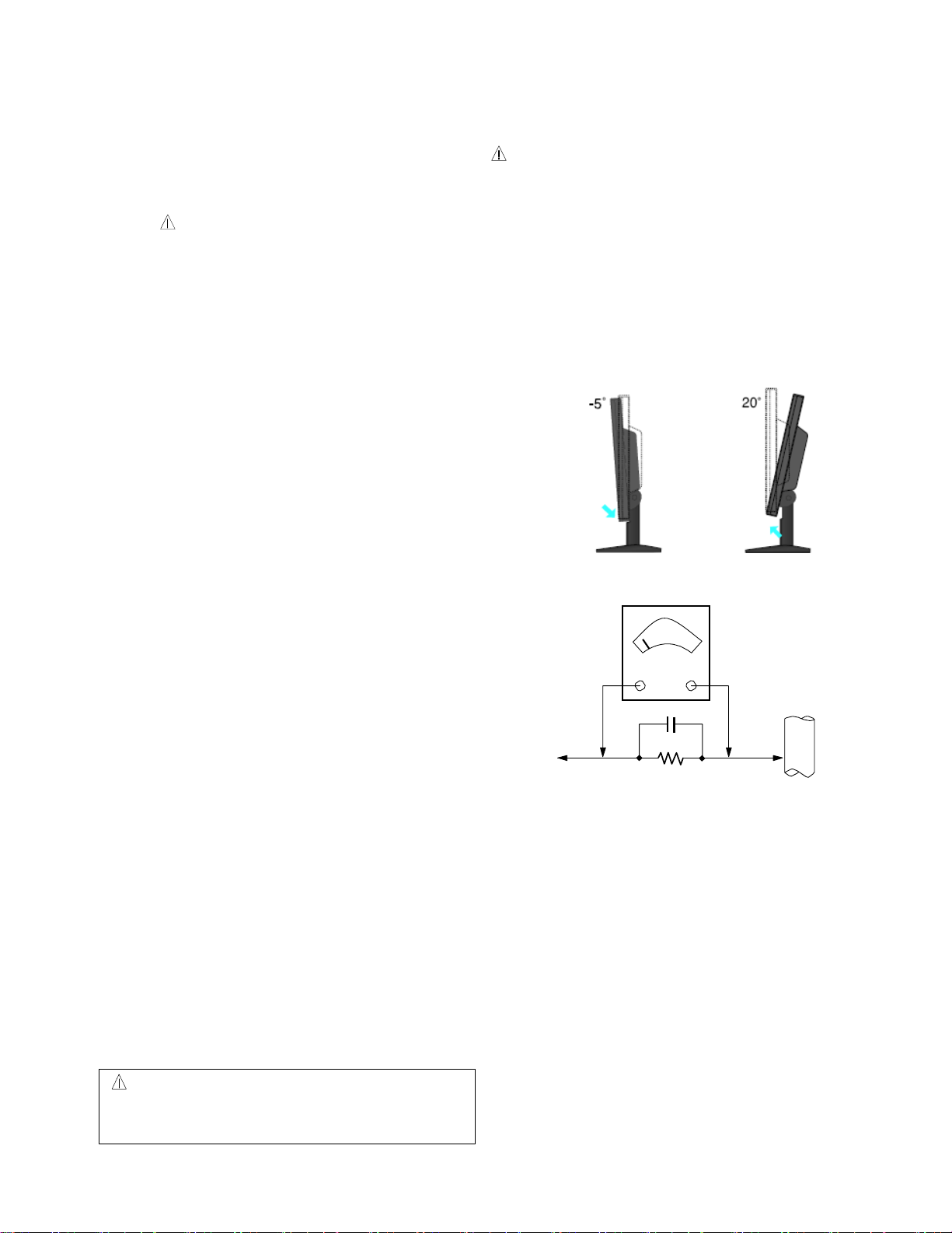
• Be careful while tilting and rotating the monitor to
avoid pinching hand(s)
Leakage Current Hot Check Circuit
AC Volt-meter
Good Earth Ground
To Instrument's
exposed METALLIC
PARTS
1.5 Kohm/10W
such as WATER PIPE,
CONDUIT etc.
CAUT ION
Please use only a plastic screwdriver to protect
yourself from shock hazard during service operation.
3
Page 4

SERVICING PRECAUTIONS
CAUTION: Before servicing receivers covered by this
service manual and its supplements and addenda, read
and follow the SAFETY PRECAUTIONS on page 3 of this
publication.
NOTE:
between the following servicing precautions and any of the
safety precautions on page 3 of this publication, always
follow the safety precautions. Remember: Safety First.
General Servicing Precautions
1. Always unplug the receiver AC power cord from the AC
2. Test high voltage only by measuring it with an
3. Discharge the picture tube anode only by (a) first
4. Do not spray chemicals on or near this receiver or any of
5. Unless specified otherwise in this service manual,
6. Do not defeat any plug/socket B+ voltage interlocks
7. Do not apply AC power to this instrument and/or any of
8. Always connect the test receiver ground lead to the
If unforeseen circumstances create conflict
power source before;
a. Removing or reinstalling any component, circuit
board module or any other receiver assembly.
b. Disconnecting or reconnecting any receiver electrical
plug or other electrical connection.
c. Connecting a test substitute in parallel with an
electrolytic capacitor in the receiver.
CAUTION: A wrong part substitution or incorrect
polarity installation of electrolytic capacitors may
result in an explosion hazard.
d. Discharging the picture tube anode.
appropriate high voltage meter or other voltage
measuring device (DVM, FETVOM, etc) equipped with a
suitable high voltage probe.
Do not test high voltage by "drawing an arc".
connecting one end of an insulated clip lead to the
degaussing or kine aquadag grounding system shield
at the point where the picture tube socket ground lead is
connected, and then (b) touch the other end of the
insulated clip lead to the picture tube anode button,
using an insulating handle to avoid personal contact
with high voltage.
its assemblies.
clean electrical contacts only by applying the following
mixture to the contacts with a pipe cleaner, cottontipped stick or comparable non-abrasive applicator;
10% (by volume) Acetone and 90% (by volume)
isopropyl alcohol (90%-99% strength)
CAUTION: This is a flammable mixture.
Unless specified otherwise in this service manual,
lubrication of contacts in not required.
with which receivers covered by this service manual
might be equipped.
its electrical assemblies unless all solid-state device
heat sinks are correctly installed.
receiver chassis ground before connecting the test
receiver positive lead.
Always remove the test receiver ground lead last.
9. Use with this receiver only the test fixtures specified in
this service manual.
CAUTION: Do not connect the test fixture ground strap
to any heat sink in this receiver.
Electrostatically Sensitive (ES) Devices
Some semiconductor (solid-state) devices can be
damaged easily by static electricity. Such components
commonly are called Electrostatically Sensitive (ES)
Devices. Examples of typical ES devices are integrated
circuits and some field-effect transistors
and semiconductor "chip" components. The
fol l o wi n g techniques should be used to help reduce the
incidence of component damage caused by static by static
electricity.
1. Immediately before handling any semiconductor
component or semiconductor-equipped assembly, drain
off any electrostatic charge on your body by touching a
known earth ground. Alternatively, obtain and wear a
commercially available discharging wrist strap device,
which should be removed to prevent potential shock
reasons prior to applying power to the unit under test.
2. After removing an electrical assembly equipped with
ES devices, place the assembly on a conductive
surface such as aluminum foil, to prevent electrostatic
charge buildup or exposure of the assembly.
3. Use only a grounded-tip soldering iron to solder or
unsolder ES devices.
4. Use only an anti-static type solder removal device.
Some solder removal devices not classified as "antistatic" can generate electrical charges sufficient to
damage ES devices.
5. Do not use freon-propelled chemicals. These can
generate electrical charges sufficient to damage ES
devices.
6. Do not remove a replacement ES device from its
protective package until immediately before you are
ready to install it. (Most replacement ES devices are
packaged with leads electrically shorted together by
conductive foam, aluminum foil or comparable
conductive material).
7. Immediately before removing the protective material
from the leads of a replacement ES device, touch the
protective material to the chassis or circuit assembly
into which the device will be installed.
CAUTION: Be sure no power is applied to the chassis
or circuit, and observe all other safety precautions.
8. Minimize bodily motions when handling unpackaged
replacement ES devices. (Otherwise harmless motion
such as the brushing together of your clothes fabric or
the lifting of your foot from a carpeted floor
can generate static electricity sufficient to damage an
ES device.)
4
Page 5

General Soldering Guidelines
1. Use a grounded-tip, low-wattage soldering iron and
appropriate tip size and shape that will maintain tip
temperature within the range or 500。F to 600。F.
2. Use an appropriate gauge of RMA resin-core solder
composed of 60 parts tin/40 parts lead.
3. Keep the soldering iron tip clean and well tinned.
4. Thoroughly clean the surfaces to be soldered. Use a
mall wire-bristle (0.5 inch, or 1.25cm) brush with a
metal handle.
Do not use freon-propelled spray-on cleaners.
5. Use the following unsoldering technique
a. Allow the soldering iron tip to reach normal
temperature.
(500。F to 600。F)
b. Heat the component lead until the solder melts.
c. Quickly draw the melted solder with an anti-static,
suction-type solder removal device or with solder
braid.
CAUTION: Work quickly to avoid overheating the
circuitboard printed foil.
6. Use the following soldering technique.
a. Allow the soldering iron tip to reach a normal
temperature (500。F to 600。F)
b. First, hold the soldering iron tip and solder the strand
against the component lead until the solder melts.
c. Quickly move the soldering iron tip to the junction of
the component lead and the printed circuit foil, and
hold it there only until the solder flows onto and
around both the component lead and the foil.
CAUTION: Work quickly to avoid overheating the
circuit board printed foil.
d. Closely inspect the solder area and remove any
excess or splashed solder with a small wire-bristle
brush.
IC Remove/Replacement
Some chassis circuit boards have slotted holes (oblong)
through which the IC leads are inserted and then bent flat
against the circuit foil. When holes are the slotted type,
the following technique should be used to remove and
replace the IC. When working with boards using the
familiar round hole, use the standard technique as
outlined in paragraphs 5 and 6 above.
Removal
1. Desolder and straighten each IC lead in one operation
by gently prying up on the lead with the soldering iron
tip as the solder melts.
2. Draw away the melted solder with an anti-static
suction-type solder removal device (or with solder
braid) before removing the IC.
Replacement
1. Carefully insert the replacement IC in the circuit board.
2. Carefully bend each IC lead against the circuit foil pad
and solder it.
3. Clean the soldered areas with a small wire-bristle
brush. (It is not necessary to reapply acrylic coating to
the areas).
"Small-Signal" Discrete Transistor
Removal/Replacement
1. Remove the defective transistor by clipping its leads as
close as possible to the component body.
2. Bend into a "U" shape the end of each of three leads
remaining on the circuit board.
3. Bend into a "U" shape the replacement transistor leads.
4. Connect the replacement transistor leads to the
corresponding leads extending from the circuit board
and crimp the "U" with long nose pliers to insure metal
to metal contact then solder each connection.
Power Output, Transistor Device
Removal/Replacement
1. Heat and remove all solder from around the transistor
leads.
2. Remove the heat sink mounting screw (if so equipped).
3. Carefully remove the transistor from the heat sink of the
circuit board.
4. Insert new transistor in the circuit board.
5. Solder each transistor lead, and clip off excess lead.
6. Replace heat sink.
Diode Removal/Replacement
1. Remove defective diode by clipping its leads as close
as possible to diode body.
2. Bend the two remaining leads perpendicular y to the
circuit board.
3. Observing diode polarity, wrap each lead of the new
diode around the corresponding lead on the circuit
board.
4. Securely crimp each connection and solder it.
5. Inspect (on the circuit board copper side) the
solder joints of the two "original" leads. If they are not
shiny, reheat them and if necessary, apply additional
solder.
Fuse and Conventional Resistor
Removal/Replacement
1. Clip each fuse or resistor lead at top of the circuit board
hollow stake.
2. Securely crimp the leads of replacement component
around notch at stake top.
3. Solder the connections.
CAUTION: Maintain original spacing between the
replaced component and adjacent components and the
circuit board to prevent excessive component temperatures.
5
Page 6

Circuit Board Foil Repair
Excessive heat applied to the copper foil of any printed
circuit board will weaken the adhesive that bonds the foil to
the circuit board causing the foil to separate from or
"lift-off" the board. The following guidelines and
procedures should be followed whenever this condition is
encountered.
At IC Connections
To repair a defective copper pattern at IC connections use
the following procedure to install a jumper wire on the
copper pattern side of the circuit board. (Use this
technique only on IC connections).
1. Carefully remove the damaged copper pattern with a
sharp knife. (Remove only as much copper as
absolutely necessary).
2. carefully scratch away the solder resist and acrylic
coating (if used) from the end of the remaining copper
pattern.
3. Bend a small "U" in one end of a small gauge jumper
wire and carefully crimp it around the IC pin. Solder the
IC connection.
4. Route the jumper wire along the path of the out-away
copper pattern and let it overlap the previously scraped
end of the good copper pattern. Solder the overlapped
area and clip off any excess jumper wire.
At Other Connections
Use the following technique to repair the defective copper
pattern at connections other than IC Pins. This technique
involves the installation of a jumper wire on the
component side of the circuit board.
1. Remove the defective copper pattern with a sharp
knife.
Remove at least 1/4 inch of copper, to ensure that a
hazardous condition will not exist if the jumper wire
opens.
2. Trace along the copper pattern from both sides of the
pattern break and locate the nearest component that is
directly connected to the affected copper pattern.
3. Connect insulated 20-gauge jumper wire from the lead
of the nearest component on one side of the pattern
break to the lead of the nearest component on the
other side.
Carefully crimp and solder the connections.
CAUTION: Be sure the insulated jumper wire
is dressed so the it does not touch components or
sharp edges.
6
Page 7
TIMING CHART
VIDEO
distingishme
1
2
3
4
5
6
7
8
9
10
11
12
13
14
15
16
nt
H(Pixels) +
V(Lines) -
H(Pixels) - 31.468 900 720 18 108 54
V(Lines) +
H(Pixels) - 31.469 800 640 16 96 48
V(Lines) -
H(Pixels) - 37.5 840 640 16 64 120
V(Lines) -
H(Pixels) + 37.879 1056 800 40 128 88
V(Lines) +
H(Pixels) + 46.875 1056 800 16 80 160
V(Lines) +
H(Pixels) +/- 49.725 1152 832 32 64 224
V(Lines) +/-
H(Pixels) - 48.363 1344 1024 24 136 160
V(Lines) -
H(Pixels) - 60.123 1312 1024 16 96 176
V(Lines) -
H(Pixels) +/- 68.681 1456 1152 32 128 144
V(Lines) +/-
H(Pixels) +/- 61.805 1504 1152 18 134 200
V(Lines) +/-
H(Pixels) + 63.981 1688 1280 48 112 248
V(Lines) +
H(Pixels) + 79.976 1688 1280 16 144 248
V(Lines) +
H(Pixels) + 55.5 1600 1440 48 32 80
V(Lines) -
H(Pixels) - 55.935 1904 1440 80 152 232
V(Lines) +
H(Pixels) - 70.635 1936 1440 96 152 248
V(Lines) +
Polority
SYNC
DOT
CLOCK
[MHz]
25.175
28.321
25.175
31.5
40.0
49.5
57.283
65.0
78.75
100.0
92.978
108.0
135.0
88.750
106.500
136.750
A
E
D B
C
M
Frequency
[kHz]/ [Hz]
31.469
70.8 449 350 37 2 60
70.09 449 400 12 2 35
59.94 525 480 10 2 33
75 500 480 1 3 16
60.317 628 600 1 4 23
75.0 625 600 1 3 21
74.55 667 624 1 3 39
60.0 806 768 3 6 29
75.029 800 768 1 3 28
75.062 915 870 3 3 39
65.96 937 900 2 4 31
60.02 1066 1024 1 3 38
75.035 1066 1024 1 3 38
59.90 926 900 3 6 17
59.887 934 900 3 6 25
74.984 942 900 3 6 33
Total period
(E)
800 640 16 96 48
Display
(A)
Front
Porch
(D)
Sync.
(C)
Back
Porch
(B)
Resolution
640 x 350
720 X 400
640 x 480
640 x 480
800 x 600
800 x 600
832 x 624
1024 x 768
1024 x 768
1152 x 870
1152 x 900
1280 x
1024
1280 x
1024
1440 x 900
1440x 900
1440x 900
7
Page 8
DISASSEMBLY
#1 #2
Put a soft cushion on the desk and lay the stand on
its side so that the base is accessible.
#4
#3
Pry the hinge cover by flat-tip screw driver or jig and
be careful to prevent from scratching the hinge
cover.
Pull up the front cover side by side(4 sides) and take
away the front cover
8
Twist the stand assy until “click” , then take out the
stand assy into the product in the
correct direction as shown in picture.
Unscrew the 4 screws on the hinge to separate the
hinge neck ass’y
.
#6#5
Turn over the set and pull up the cabinet to separate
the control cable, then take away the back cover
Page 9
#8#7
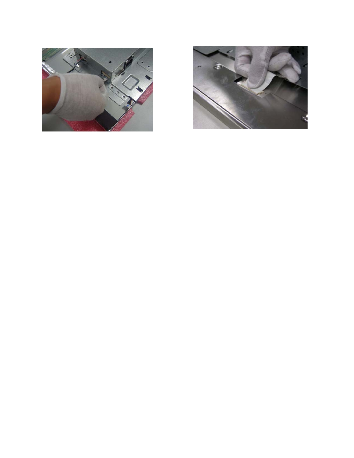
Pull out the LVDS cable Pull out the lamp wire.
9
Page 10
A
A
A
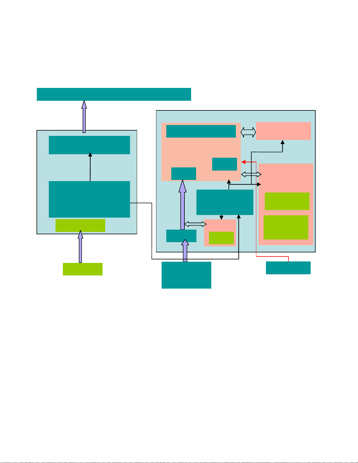
BLOCK DIAGRAM
L192WS consists of a main body and a stand (base). The main body contains a InnoLux (or CMO) LCD
module with 4 CCFL lamps, a power board (includes AC/DC, DC/DC, inverter and panel power source),
a control board (key pad) and an interface board. The block diagram is shown as below.
InnoLux TFT-LCD Module with 4FFCLs
Inverter
14V
Power
AC to DC (14V&5V)
C Socket
C Input
LVDS Transmitter
TSUM16AL-LF-1
DC
1.8V regulator
24C02
D-sub
Analog
RGB Signal
10
MCU
3.3V and
DDC
128KB Flash ROM
EEPROM
24C04
OSD parameters
Timing
parameters
Key pad
Page 11

DESCRIPTION OF BLOCK DIAGRAM
1. Video Controller Part.
This part amplifies the level of video signal for the digital conversion and converts from the analog video signal to the digital
video signal using a pixel clock.
The pixel clock for each mode is generated by the PLL. The range of the pixel clock is from 25MHz to 135MHz.
This part consists of the Scaler, ADC convertor and LVDS transmitter.
The Scaler gets the video signal converted analog to digital, interpolates input to 1440 X 900 resolution signal and outputs
8-bit R, G, B signal to transmitter.
2. Power Part.
This part consists of the one 3.3V, and one 1.8V regulators to convert power which is provided 5V in Power board.
14V is provided for inverter, 14V is provided for LCD panel and 5V for micom.
Also, 5V is converted 3.3V and 1.8V by regulator. Converted power is provided for IC in the main board. The inverter
converts from DC14V to AC 700Vrms and operates back-light lamps of module.
3. MICOM Part.
This part is include video controller part. And this part consists of EEPROM IC which stores control data, and the Micom
which imbedded in scaler IC.
The Micom distinguishes polarity and frequency of the H/V sync are supplied from signal cable. The controlled data of each
modes is stored in EEPROM.
11
Page 12
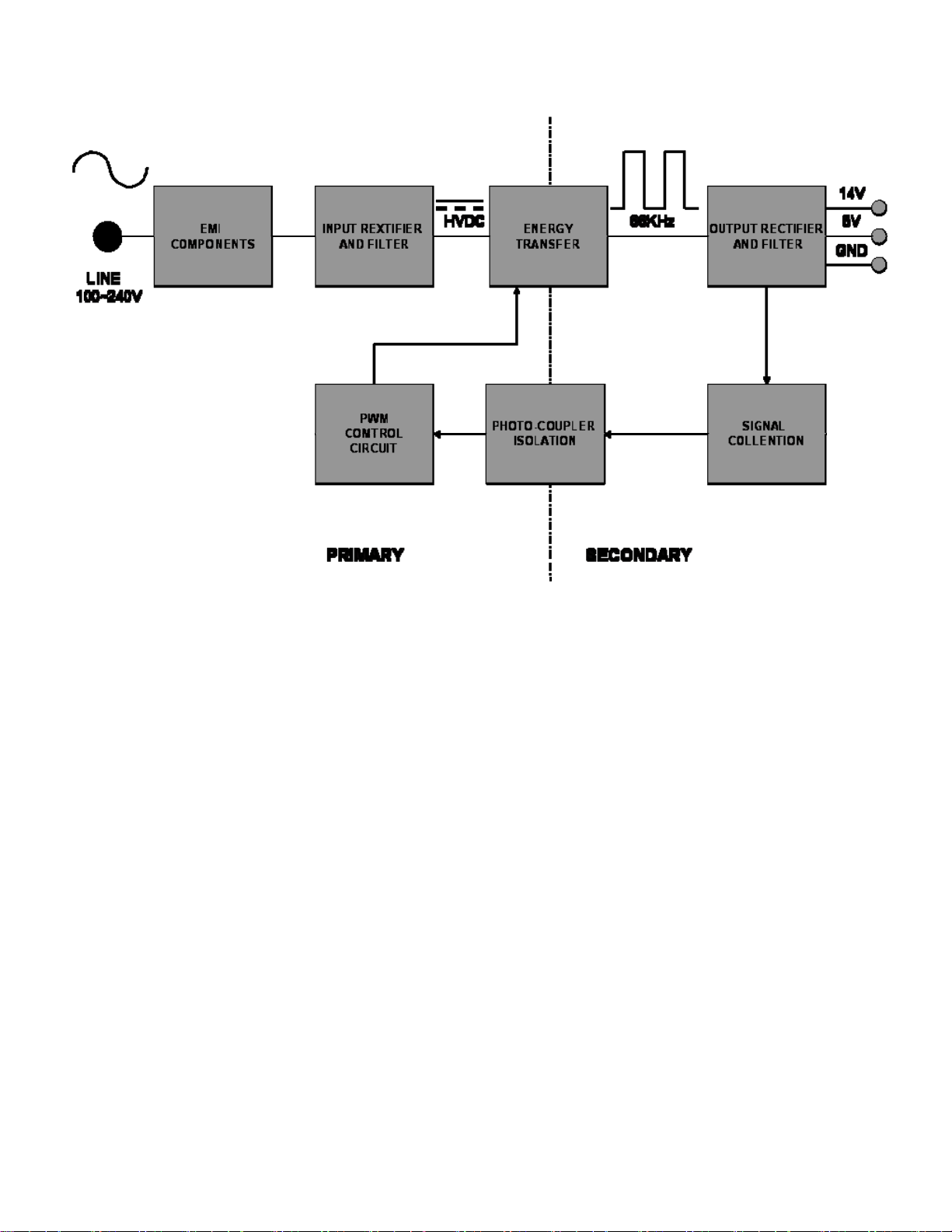
LIPS Board Block Diagram
50~60Hz
Operation description_LIPS
1. EMI components.
This part contains of EMI components to comply with global marketing EMI standards like FCC, VCCI CISPR, the circuit
included a line-filter, across line capacitor and of course the primary protection fuse.
2. Input rectifier and filter.
This part function is for transfer the input AC voltage to a DC voltage through a bridge rectifier and a bulk capacitor.
3. Energy Transfer.
This part function is transfer the primary energy to secondary through a power transformer.
4. Output rectifier and filter.
This part function is to make a pulse width modulation control and to provide the driver signal to power switch, to adjust
the duty cycle during different AC input and output loading condition to achive the dc output stablize, and also the over
power protection is also monitor by this part.
5. Photo-Coupler isolation.
This part function is to feed back the dc output changing status through a photo transistor to primary controller to achieve
the stabilized dc output voltage.
6. Signal collection.
This part function is to collect the any change from the dc output and feed back to the primary through photo transistor.
12
Page 13

ADJUSTMENT
Windows EDID V1.0 User Manual
Operating System: MS Windows 98, 2000, XP
Port Setup: Windows 98 => Don’t need setup
Windows 2000, XP => Need to Port Setup.
This program is available to LCD Monitor only.
1. Port Setup
a) Copy “UserPort.sys” file to
“c:\WINNT\system32\drivers” folder
b) Run Userport.exe
2. EDID Read & Write
1) Run WinEDID.exe
c) Remove all default number
d) Add 300-3FF
e) Click Start button. f)
Click Exit button.
2) Edit Week of Manufacture, Year of Manufacture,
Serial Number
a) Input User Info Data
b) Click “Update” button
c) Click “ Write” button
13
Page 14

SERVICE OSD
o
1) Turn off the power switch at the front side of the display.
2) Wait for about 5 seconds and press MENU, POWER switch with 1 second interval.
3) The SVC OSD menu contains additional menus that the User OSD menu as described below.
a) Auto Color : W/B balance and Automatically sets the gain and offset value.
b) NVRAM INIT : EEPROM initialize.(24C04)
c) CLEAR ETI : To initialize using time.
d) AGING : Select Aging mode(on/off).
e) R/G/B-9300K : Allows you to set the R/G/B-9300K value manually.
f) R/G/B-6500K : Allows you to set the R/G/B-6500K value manually.
g) R/G/B-Offset : Allows you to set the R/G/B-Offset value manually.(Analog Only)
h) R/G/B-Gain : Allows you to set the R/G/B-Gain value manually.(Analog Only)
i) MODULE : Show Current module Type
j)RS232: Enable/Disable Debug Mode(on/off)
Insert to
Parallel Port
n PC
ISP Board
Parallel
Port
15PIN
D-SUB
LCD
Monitor DSub
Figure 1.Cable Connection For ISP
14
Page 15

TROUBLESHOOTING GUIDE
1. No Power & Power LED Off
No power
Check primary
rectifier voltage
Check circuit
if short
Check IC802,
C805, T801
Check F801, P801,
D801
Check pin3 of
IC802 voltage
about 1V
Check R801, R805,
R822, R823, R817
Check pin2 of IC802
voltage about 2V
Check R803, R807,
R824, R825
Check pin1 of IC802
voltage is 5.8V
Check R812, R816,
C818
END
15
Page 16

2. Backlight can’t be turned on
No raster?
Backlight can’t
be turned on.
Is there 5Vdc
voltage on pin2 of
IC501?
Is there high-level voltage
on pin10 of IC501?
Are connected rightly
CN501, CN502, CN503 and
CN504?
Is there instantaneously pulse wave on
pin1, pin3, pin15 of IC501 at the
moment of restart?
Check feedback circuit
Isen,Vsen.(D501,D502.D503,D504,D507,D508)
Check power
supply
16
Is Ok IC501?
No
Check I/F
board
R526 open
Connecting the
output connector
again
U501, U502 fail
IC501 fail
T501, T502 fail
Page 17

t
3. DC output voltage is unstable
1. Output Voltage
Unstable
Check Vbe of
Q801 below 0.3V
Check reference
voltage
Check feedback
circui
END
Check circuit if
short
Check Q801, Q802
Check Pin R of
IC803 voltage
Check R810, R811
Check Vpin3-4 of
IC801 about 6V
Check Vpin1-2 of
IC801 about 1V
Check R809,
R814
17
Check ZD801, ZD802,
ZD803, D803, D805
Check R809, R814,
IC801, R818
Check C815, D806,
R812
Page 18

4.Output power is unstable
5
Unstable power
Check sampling
Circuit
Check the R pin
voltage of IC803
about 2.
V
Check pin1 of
IC802 voltage
is 5.8V
Check pin3 of
IC802 voltage
about 1V
END
Check R810,
R811, R818
Check the C pin
voltage of IC803
if 3V
Check R809, R808, R814,
D809
Check D806, C815 if
short
Change
D806, C815
Change R801, R805,
R822, R823, R817
18
Change R810,
R811, R818
Change
IC803
Page 19

5.Black Screen and backlight turn on
Black Screen
Check power supply:
Pin1, 2 of CN101
NG
Power Fail
OK
Check pin34, 51, 66, and 82
Of U105
NG
Check FB103
And U102
OK
NG
Check pin32, 49, 56, and 75
Of U105
OK
Check FB106
And U101
Check Reset (pin84)
Of U105
NG
Check C144, R172
OK
Check Crystal: Pin96,
Pin97
Of U105
NG
Check: X101,
C153, C154
OK
Check CCFL - Enable
OK OK
(pin85) of U105
Check pin5 of
CN101
Inverter Fail
NG
MCU (imbedded in
Scaler IC) Fail
NG
Check R167, Q106
R108, R110
19
Page 20

6.White Screen
White Screen
LVDS Cable
Reinsert
OK
Workmanship
NG
Change LVDS
Cable
OK
LVDS Cable NG
NG
Check VLCD
Is 5V?
OK OK
Check LVDS
Signals
Panel Fail
NG
NG
Check Panel - Enable
Of U105 (pin48) is High?
Check the HW Reset
Of U105 pin84
NG
Check C144
,R172
OK
NG
Check R168, R105
Q103, Q101
OK
Check the pins
Of U105
END
20
Page 21

7. BAD SCREEN
OK
OK
OK
NG
21
Bad Screen
NG
Change LVDS Cable
NG
Check Crystal:Pin96,97
Of U105
OK
Check the communication
Of U105 and U106
OK
Check the pins of
U105 and U106
WorkmanshipLVDS Cable Reinsert
LVDS Cable NG
Check :X101,
C153,C154
Check: SDO,SCZ,
SCK,SDI, Reset
Page 22

WIRING DIAGRAM
22
Page 23

- 23 -
EXPLODED VIEW
140
130
120
110
160
100
090
080
150
050
070
060
170
040
030
020
010
Page 24

EXPLODED VIEW PARTS LIST
Ref.No. LGE Part No. INL Part No. Description
ABJ32903501
010
ABJ32903502
020
MKC37547001
EBU36594401
030
EBU36577201
040
EBU36576401
EBU36589602
050
EBU36589601
060
ADV32904101
070
EBU36589701
080
MEY37547401
090
MEY37547601
100
ACQ32904401
110
ACQ32904601
120
ACQ32904701
130
MCK37548201
140
MCK37548401
150
EBU36589801
6410TUW008A
501010209600R BEZEL,FRONT(Silver cabinet),LE1957(L192WS-SNQ)
501010209610R BEZEL,FRONT(Black cabinet),LE1957(L192WS-BNQ)
501120105100R LENS(T),LE1957(L192WS)
631102090821R LCP 19" MT190AW01-V2- G1,AM1900004201(INL)
631102090650R LCD PANEL 19"M190A1-L02(A)(CMO)ROHS
790841400600R PCBA,P/I BOARD,LE1957(L192WS)-610 ROHS
790841300600R
790841300500R
701000003000R ASSY,CHASSIS,LE1957
790841500000R PCBA,KEYPAD BOARD,LE1957 ROHS
501030205700R BUTTON,FUNCTION KEY(B),LE1957,ROHS
501030205710R BUTTON,POWER KEY(B), LE1957 ROHS
714020008900R ASSY,BASE(B),LE1957
714010009300R ASSY,STAND(B),LE1957
714010009310R ASSY,STAND NECK,LE1957
501020212000R COVER,HINGE(B),LE1957,ROHS
501020211900R COVER,BACK(B),LE1957,ROHS
430303000730R HRN LVDS FFC 30P 155mm ACCP30155MU28MY
453070800150R
PCBA,I/F BOARD(V2),LE1957-610 ROHS (For InnoLux ModuleL192WS-SNQ/BNQ. A**JQP)
PCBA,I/F BOARD,LE1957-510 ROHS (For CMO Module –
L192WS-SNQ/BNQ.A**QQP)
PWR CORD 10A/125V BLK 6FT UL/CSA,SVT 3Cx
---US/Mexico/Panama/Canada
PWRCORD 10A/250V BLK 6FT UK,H05VV-F 3Cx0
---UK/Malaysia/Singapore
PWRCORD 16A/250V BLK 6FT VDE,H05VV-F 3Cx
---Europe/Thailand/Vietnam/Russia/U.A.E
PWRCORD 10A/250V BLK 1850mm SAA,H05W-F 3
---Australia
PWRCORD 7A/125V BLK 1850mm CNS,VCTF 3Gx0
---Taiwan
160
170
EBU36590701
6410TBW004A
6410TEW003A
6410TSW003A
6410TTW001A
453070800720R
453070800730R
453070800740R
453070800750R
430300800830R HRN ASS'Y 2*4p to 1*8p 305mm UL1571#28
24
Page 25

REPLACEMENT PARTS LIST
CAUTION: BEFORE REPLACING ANY OF THESE COMPONENTS,
READ CAREFULLY THE SAFETY PRECAUTIONS IN THIS MANUAL.
* NOTE : S SAFETY Mark
AL ALTERNATIVE PARTS
Power and Inverter PCBA Board
Item Location P/N Description
790841400600R PCBA,P/I BOARD,LE1957-610 ROHS
10 IC801, 412140002380R IC LTV817M-PR VDE (LITE-ON) P=10mm RoHS
10 RA 412140001390R IC EL817M-B(EVERLIGHT)RoHS
20 U501,U502, 410500071290R XSTR AP9971GD,N-CH,PDIP-8(APEC RoHS
20 RA 410500061271R XSTR AOP802 DUAL N-CH PDIP-8(AOS)RoHS
30 D801, 411050005020R DIO BRDG BL4-06-BF52-LF 600V/4A(FRONTIER
30 RA 411050007010R DIO BRDG KBL405G 600V/4A(TSC) RoHS
30 RA 411050005090R DIO BRDG FL406 600V/4A(PEC)RoH S
40 C804, 416194743011R CAP MEX 0.47uF 275V K X2,F15 RoHS
50 C820,C801,C806, 416202224610R CAP MEY 2200pF 400V M Y,F10mm RoHS
60 C812,C809, 420421020102R
70 C808, 420421020211R
80 C805, 420431214580R
90 C824, 416204724610R CAP MEY 4700pF 400V M Y,F10mm RoHS
100 L802,L803, 425000010530R COIL CHK 5uH 7.8X10 CHK-053 0 181085R0L
110 L801, 426000050070R CHOKE L-FILTER 12mH LIN-007 ET-20,RoHS
120 T801, 426000090510R XFMR 750u@1K,+-8%,3m,113m,SPW- 051,DIP-1
130 RT801, 432009401300R
140 F801, 430613430290R FUSE SLOW 3.15,250,Axial Lead,3.6 x10mm
150 P801, 440149000220R SKT AC 10A/250V U/C/V,G/Y=45mm TU-301-SP
160 CN501,CN502,CN503,CN504, 430637020030R
170 CN801, 430300600170R HRN ASS'Y 6P 90mm UL1007#24, ROHS
180 C525,C527, 418105058010R CAP CD SL 5pF 3KV K,F7.5 RoHS
190 C803, 418247233020R CAP CD X7R 4700pF 1KV K,W/O FO RMING,RoH
200 C524,C526, 418110058510R CAP CD SL 10pF 3KV J,F7.5 RoHS CC45SL3FD
210 T501,T502, 426000090680R XFMR SW,121.5uH EEL19M DIP SPW-068,RoHS
220 H501, 502040604500R SHIELD,EMI, LE1915 ROHS
CAP EC 1000uF/10V M,105℃ N-F 10x16(L-ES
CAP SD 1000uF 25V M,105℃ F 13x20 RoHS
CAP SEK 120uF 450V 18*40 M CF 105℃
NTC 8Ω 4A 13Φ P=7.5mm F ROHS
WFR. 2P P=3.5mm 90°W/LOCK,RoHS
230 735100007120R ASSY,H/S,SBR10U100CT/U40CT, LE1710
240 735100005900R ASSY,H/S TOP246Y, LE1X09 ROHS
250 790841440600R PCBA,P/I BOARD,SMD,LE1957-610 ROHS
260 511130001201R SOLDER BAR,Sn96.5/Ag3.0/Cu0.5(SAC305 VAC
25
Page 26

260 511130001200R SOLDER BAR,Sn96.5/Ag3.0/Cu0.5/Ni0.06/Ge0
270 511110000101R HOT-MELT ADHESIVES (#526)
280 511110000501R SILICONE RTV RUBBER,UB-511(EURO)
Item Location P/N Description
735100005900R ASSY,H/S TOP246Y, LE1X09 ROHS
10 IC802, 412000379270R IC TOP246YN,TO-220-7C(POWER IN TEGRATION
20 507200003700R HEATSINK,46x20xt10mm LE1704/05
30 509112306100R SCREW,P,CROSS,T.T-3*6,ZnROHS
Item Location P/N Description
735100007120R ASSY,H/S,SBR10U100CT/U40CT, LE1710
10 D803, 411090009480R SCHTKY SP10100C 100V/10A ITO220(WILLAS)R
10 RA 411090041010R SCHTKY SRF10100 100V/10A ITO220AB(TSC)Ro
20 D805, 411090024480R SCHTKY SP1040C 40V/10A ITO220(WILLAS)RoH
20 RA 411090040010R SCHTKY SRF1050 50V/10A ITO220AB(TSC)RoHS
20 RA 411090024010R SCHTKY SRF1040 40V/10A ITO220AB(TSC)RoHS
30 507200003800R HEATSINK,56x20xt10mm LE1904/05
40 509112306100R SCREW,P,CROSS,T.T-3*6,ZnROHS
Item Location P/N Description
790841440600R PCBA,P/I BOARD,SMD,LE1957-610 ROHS
10 Q801, 410500045210R XSTR PMBT3904 NPN 200MA,40V SOT23(PHILIP
10 RA 410500045140R XSTR MMBT3904LT1G NPN 200MA 40V SOT23(ON
10 RA 410500045090R XSTR MMBT3904 NPN SOT-23(PANJIT)RoHS
20 IC501, 412000455630R IC OZ9938GN SOIC16(O2 MICRO)RoHS
30 D501,D502,D503,D504,D507,D508, 411020026210R DIO BAV99 350mW 70V SOT-23(PHI RoHS
30 RA 411020026390R DIO BAV99,SOT-23(INFINEON)RoHS
30 RA 411020026020R DIO BAV99-LF 350mW 70V SOT-23 (FEC)RoHS
30 RA 411020026090R DIO BAV99 350mW 75V SOT-23(PEC RoHS
40 D505,D506, 411020068020R DIO BAW56 70V SOT-23(FRONTIER)RoHS
40 RA 411020068090R DIO BAW56 75V SOT-23(PANJIT)RoHS
40 RA 411020068210R DIO BAW56 85V SOT-23(PHILIPS)RoHS
50 ZD803, 411100956920R ZENER 5.6V MMSZ5232A SOD123(PE C)RoHS
50 RA 411131556920R ZENER 5.6V 0.5W DDZ5V6B-F,SOD1 23(DIODES
50 RA 411131456920R ZENER 5.6V MMSZ5232A SOD-123(WILLAS)ROHS
60 ZD801, 411100991950R ZENER 9.1V MMSZ5239B SOD123(PE C)RoHS
60 RA 411131591952R ZENER 9.1V 0.5W DDZ9V1C-F,SOD1 23(DIODES
60 RA 411131491920R ZENER 9.1V MMSZ5239A SOD-123(WILLAS)ROHS
70 ZD804, 411100916020R ZENER 16V MMSZ5246A SOD123(PEC RoHS
26
Page 27

70 RA 411131516052R ZENER 16V 0.5W DDZ16-F,SOD123(DIODES)RoH
70 RA 411131416020R ZENER 16V MMSZ5246A SOD-123(WILLAS)ROHS
80 ZD805, 411100912020R ZENER 12V MMSZ5242A SOD123(PEC RoHS
80 RA 411131512052R ZENER 12V 0.5W DDZ12C-F,SOD123 (DIODES)R
80 RA 411131412020R ZENER 12V MMSZ5242A SOD-123(WILLAS)ROHS
90 R511,R510, 414916033050R
100 R802,R806, 414904010050R
110 R809, 414904100010R
120 R813,R814,R815, 414908010250R
130 R512,R526, 414916010350R
140 R808,R819,R827, 414908010350R
150 R514, 414916010450R
160 R513,R529,R530, 414916010550R
170 R817, 414908120210R RES SMD (0805) 12K F RT RoHS REV:A
180 R829, 414908020150R
190 R534, 414916220110R
200 R524, 414916220210R
210 R506,R508,R532,R533, 414908033050R
220 R818,R517,R520, 414908330110R
230 R523, 414916330210R
240 R527, 414916330410R RES SMD (0603) 3.3M F RT RoHS
250 R801,R805,R822,R823, 414908033550R
270 R522, 414916453210R
280 R509,R539,R540,R541,R542, 414916470010R
290 R825, 414908047450R
300 R810, 414908510110R
310 R811, 414908510210R
320 R803,R807,R824, 414908051450R
330 R538, 414916604310R
340 R816, 414908068950R
350 R535, 414908075150R
360 C504, 419311020060R C SMD(0603) X7R 1000PF/50V K RoHS
RES SMD (0603) 33Ω J,RT RoHS REV:A
RES SMD (1206) 10Ω J,RT RoHS
RES SMD (1206) 100Ω F,RT RoHS
RES SMD (0805) 1KΩ J,RT RoHS REV:A
RES SMD (0603) 10KΩ J,RT RoHS
RES SMD (0805) 10KΩ J,RT RoHS REV:A
RES SMD (0603) 100KΩ J,RT REV:A RoHS
RES SMD (0603) 1MΩ J,RT RoHS REV:A
RES SMD (0805) 200Ω J,RT RoHS
RES SMD (0603) 2.2KΩ F,RT RoHS
RES SMD (0603) 22KΩ F,RT RoHS
RES SMD (0805) 33Ω J,RT RoHS
RES SMD (0805) 3.3KΩ F,RT RoHS REV:A
RES SMD (0603) 33KΩ F,RT RoHS
RES SMD(0805) 3.3MΩ J,RT,RoHS
RES SMD (0603) 45.3KΩ F RT ROHS
RES SMD (0603) 470Ω F,RT RoHS
RES SMD (0805) 470KΩ J,RT RoHS
RES SMD (0805) 5.1KΩ F,RT RoHS
RES SMD (0805) 51KΩ F,RT RoHS
RES SMD (0805) 510KΩ J,RT RoHS
RES SMD (0603) 604KΩ F,RT RoHS
RES SMD (0805) 6.8Ω J RT RoHS
RES SMD (0805) 750Ω J,RT RoHS REV:A
370 C501,C502,C513,C514,C535,C536, 419311020070R C SMD(0805) X7R 1000PF/50V K RoHS
380 C505, 419311030060R C SMD(0603) X7R 0.01uF/50V K RoHS
390 C821, 419311040060R C SMD(0603) X7R 0.1uF/50V K RoHS
400 C531, 419301810560R C SMD(0603) NPO 180PF/50V J RoHS REV:A
410 C511,C507, 419342254670R C SMD(0805) Y5V 2.2uF/16V Z RoHS
420 C529, 419302710560R C SMD(0603) NPO 270PF/50V J RoHS REV:A
430 C508,C512,C516, 419313333060R C SMD(0603) X7R 0.033uF/25V K RoHS
450 C506, 419314720060R C SMD(0603) X7R 4700PF/50V K RoHS
27
Page 28

460 C523,C530, 419316820070R C SMD(0805) X7R 6800PF/50V K RoHS
470 C510,C532, 419316830060R C SMD (0603) X7R 0.068uF 50V,K RoHS
480 790841410600R PCBA,P/I BOARD,AI,LE1957-610 ROHS
Item Location P/N Description
790841410600R PCBA,P/I BOARD,AI,LE1957-610 ROHS
10 790841450600R PCBA,P/I BOARD,AI/A,LE1957-610 ROHS
20 790841460600R PCBA,P/I BOARD,AI/R,LE1957-610 ROHS
Item Location P/N Description
790841450600R PCBA,P/I BOARD,AI/A,LE1957-610 ROHS
10 R828, 415340101540R
20 R820,R821, 415030105540R
30 R503,R501, 414870305540R
40 R521, 415020330540R
50 R812, 414020689540R
60 R804, 415130680540R
70 D806, 411020052020R DIO A02-LF 200V/1A R1(FEC)RoHS
70 RA 411030003040R DIO FR103 200V/1A DO-41(MOSPEC RoHS
70 RA 411030065090R DIO PS102R 200V/1A DO-41(PEC)ROHS
80 D809, 411022003210R DIO 1N4148 75V/0.2A AT (PHIL) RoHS
80 RA 411022003020R DIO 1N4148-LF 75V/0.15A AT (FEC)RoHS
80 RA 411020048090R DIO 1N4148-35 75V/0.15A,DO35(P EC)RoHS
90 D804, 411020053090R DIO PS1010R 1000V/1A DO-41(PAN JIT)RoHS
90 RA 411032006020R DIO FR10-10-LF 1000V/1A AT(FRO NTIER)RoH
100 ZD802, 411020050090R DIO P6KE150A,DO-15,AT(PANJIT)RoHS
100 RA 411020050020R DIO P6KE150A-LF AT(FRONTIER) RoHS
100 RA 411020050010R DIO P6KE150A,DO-15AT,(TSC)RoHS
110 F802, 430613040100R FUSE SLOW PICO II 4A/125V U/C,AT,RoHS
RES MOF 1W 100Ω J,AT MINI RoHS
RES CF 1/2W 1MΩ J,AT MINI RoHS
RES MG HV 1/2Ws 3MΩ 3KV J,AT RoHS
RES CF 1/4W 33Ω J,AT MINI RoHS
RES FSM 1/4W 6.8Ω J AT MINI,RoHS
RES CF 1/2W 68Ω J,AT RoHS REV:A
120 J502,J503,J510,J511,J514,J804,J805,J809, 430405000000R JMPR ROLL/KG D=0.6mm,AT,RoHS 7.5MM
120 RA 430405000000R JMPR ROLL/KG D=0.6mm,AT,RoHS 7.5MM
130 J501,J504,J512,J513,J803,J808, 430405000000R JMPR ROLL/KG D=0.6mm,AT,RoHS 10MM
130 RA 430405000000R JMPR ROLL/KG D=0.6mm,AT,RoHS 10MM
140 J506,J509,J810,J812, 430405000000R JMPR ROLL/KG D=0.6mm,AT,RoHS 12.5MM
140 RA 430405000000R JMPR ROLL/KG D=0.6mm,AT,RoHS 12.5MM
150 J507,J508, 430405000000R JMPR ROLL/KG D=0.6mm,AT,RoHS 15MM
150 RA 430405000000R JMPR ROLL/KG D=0.6mm,AT,RoHS 15MM
160 J802, 430405000000R JMPR ROLL/KG D=0.6mm,AT,RoHS 17.5MM
160 RA 430405000000R JMPR ROLL/KG D=0.6mm,AT,RoHS 17.5MM
170 J505, 430405000000R JMPR ROLL/KG D=0.6mm,AT,RoHS 20MM
28
Page 29

170 RA 430405000000R JMPR ROLL/KG D=0.6mm,AT,RoHS 20MM
180 506140005700R LABEL,BARCODE,BLANK,33x7mm, ROHS,FOR PCB
190 700000000300R ASSY,PCB&RIVENT,LE1957 ROHS
Item Location P/N Description
790841460600R PCBA,P/I BOARD,AI/R,LE1957-610 ROHS
10 C802,C811, 418210227030R CAP CD X7R 1000pF 500V K VT RoHS
20 C817,C822, 419111040030R CAP MTL X7R 0.1uF 50V K,VT, RoHS
30 C816, 416231041530R CAP MEB 0.1uF 100V J,(RSB),VT RSBEC3100D
30 RA 416141041531R CAP MKT 0.1uF 100V J,VT(ARCO) RoHS,R82EC
40 C522, 420421510330R
50 C509, 420422210360R
60 C813, 418147038530R CAP CD NPO 47pF 1KV J,VT RoHS
70 C814,C815,C818,C819, 420264700230R
80 C810, 420424710260R
90 Q802, 410072013210R XSTR 2PC1815GR*I VT (PHILIPS) RoHS REV:
90 RA 410072013370R XSTR 2SC1815-GR (T2SPF.T) VT (TOSHIBA)Ro
90 RA 410072013150R XSTR UTC2SC1815L-GR NPN TO92 (UTC)RoHS
100 IC803, 412022002840R IC TL431ACLPG TO-92 1%,VT(ON)RoHS
100 RA 412022002240R IC KA431AZ 1%,VT (FAIRCHILD) RoHS
CAP SD 150uF 35V M,105℃ VT 8x12 RoHS
CAP SD 220uF/35V M 105℃ ST,10x13,RoHS
CAP SH 47uF 25V M,125℃,VT, 6.3x11,RoHS
CAP SD 470uF/25V M 105℃ ST 10x16,RoHS
100 RA 412022002300R IC AP431VL TO-92 1% VT (ATC) RoHS
100 RA 412022002830R IC AS431 TO-92 VT(A1SEMI)RoHS
Item Location P/N Description
700000000300R ASSY,PCB&RIVENT,LE1957 ROHS
10 490831400100R PCB,P/I BOARD,LE1957 ROHS
20 M3,M4,M5,M6,M7,M8, 512006000500R
30 M1,M2, 512006000600R
RIVET,Φ 3.0xΦ 1.6x3.0mm
RIVET,Φ 4.1xΦ 2.2x3.0mm
Control PCBA Board
Item Location P/N Description
790841500000R PCBA,KEYPAD BOARD,LE1957 ROHS
10 LED101, 411070089450R
20 SW101,SW102,SW103,SW104,SW105, 430602980120R SW TACT 160gf 1P,H=4.3mm,DIP SFKHHAL2420
30 CN101, 430300800840R HRN ASS'Y 8p 65mm UL1571#28
40 490831500100R PCB,KEYPAD BOARD,LE1957 ROHS
50 511130001201R SOLDER BAR,Sn96.5/Ag3.0/Cu0.5(SAC305 VAC
50 511130001200R SOLDER BAR,Sn96.5/Ag3.0/Cu0.5/Ni0.06/Ge0
60 502110400100R SPRING SHEET, LE1730
LED Y/G∮3x5mm HTL-7VYVG4B1F-D12-FB-LC4.
29
Page 30

Main PCBA Board
For INL Module
Item Location P/N Description
790841300600R PCBA,I/F BOARD(V2),LE1957-610 ROHS
10 629030009400R PROGRAM(V2),LE1957-610 ROHS
20 790841320600R PCBA,I/F BOARD,MI,LE1957-610 ROHS
30 790841340600R PCBA,I/F BOARD,SMD,LE1957-610 ROHS
40 511130001201R SOLDER BAR,Sn96.5/Ag3.0/Cu0.5(SAC305 VAC
40 RA 511130001200R SOLDER BAR,Sn96.5/Ag3.0/Cu0.5/Ni0.06/Ge0
50 506440003800R LABEL,BLANK,YELLOW,10x4mm
Item Location P/N Description
790841320600R PCBA,I/F BOARD,MI,LE1957-610 ROHS
10 C111,C144, 420431000260R
20 C101,C102, 420431010461R
30 C130,C133,C142,C145,C105, 420432200460R
40 C108, 420432210460R
50 CN101, 430631060020R
60 CN105, 430631080130R WAFER 2x4P 2.0mm,200PHD-2*4ST RoHS
70 X101, 432008010370R XTAL 14.31818MHz 16pF HC-49US 30PPM,DIP,
80 CN103, 440819015030R CON,D-SUB,FEM.15P RA W/O SCREW DZ11AA1-H
Item Location P/N Description
790841340600R PCBA,I/F BOARD,SMD,LE1957-610 ROHS
10 Q103,Q106, 410500045210R XSTR PMBT3904 NPN 200MA,40V SOT23(PHILIP
10 RA 410500045140R XSTR MMBT3904LT1G NPN 200MA 40V SOT23(ON
10 RA 410500045090R XSTR MMBT3904 NPN SOT-23(PANJIT)RoHS
20 Q102,Q105, 410500046210R XSTR PMBT3906 PNP 200MA,40V SOT23(PHILIP
20 RA 410500046180R XSTR MMBT3906LT1G PNP 200mA 40V SOT23(ON
20 RA 410500046090R XSTR MMBT3906 PNP SOT-23(PANJIT)RoHS
30 Q101, 410500068290R XSTR AP2305GN P-CH SOT23(APEC) RoHS
30 RA 410500075270R XSTR AO3415 P-CH,SOT23(AOS) RoHS
40 Q107, 410500050210R XSTR 2N7002,N-CH FET SOT-23 (PHILIPS)RoH
40 RA 410500050130R XSTR SN7002N N-CH SOT-23(INFINEON),RoHS
40 RA 410500050090R XSTR 2N7002 N-CH SOT-23(PANJIT)RoHS
50 TVS101,TVS102,TVS103,TVS104, 411020026210R DIO BAV99 350mW 70V SOT-23(PHI RoHS
50 RA 411020026020R DIO BAV99-LF 350mW 70V SOT-23 (FEC)RoHS
50 RA 411020026390R DIO BAV99,SOT-23(INFINEON)RoHS
50 RA 411020026090R DIO BAV99 350mW 75V SOT-23(PEC RoHS
60 D103, 411020047210R DIO BAV70 85V SOT23 (PHILIPS) RoHS
CAP EC 10uF 25V M,105℃ ST 5x11 RoHS
CAP EC 100uF 16V M,105℃ ST 5x11(SK) RoH
CAP EC 22uF 16V M,105℃ ST, 5x11,RoHS
CAP EC 220uF 16V M,105℃ ST 6.3x11 RoHS
WAFER 2.0mm 6P 180°,RoHS
30
Page 31

60 RA 411020047020R DIO BAV70-LF, 70V SOT-23(FEC) ROHS
60 RA 411020047090R DIO BAV70, 70V SOT-23(PEC) ROHS
70 ZD101,ZD105,ZD106,ZD107,ZD108, 411100956920R ZENER 5.6V MMSZ5232A SOD123(PE C)RoHS
70 RA 411131556920R ZENER 5.6V 0.5W DDZ5V6B-F,SOD1 23(DIODES
70 RA 411131456920R ZENER 5.6V MMSZ5232A SOD-123(WILLAS)ROHS
80 U108, 412000279480R IC AT24C04N-10SU-2.7 SOP8 4K(A TMEL)RoHS
80 RA 412000279280R IC M24C04-WMN6TP4K SOP8 (ST) RoHS
80 RA 412000479990R IC CAT24C04WI-TE13 SOIC-8(CATALYST)RoHS
90 U102, 412000330830R IC AS1117L-1.8/TR-LF,SOT223(A1 SEMI)RoHS
90 RA 412000330020R IC LD1117AL-1.8V-A SOT223(UTC) RoHS
90 RA 412000330070R IC AZ1117H-1.8 SOT223(AAC)RoHS
100 U101, 412000372830R IC AS1117L-3.3TR-LF,SOT223(A1S EMI)RoHS
100 RA 412000372020R IC LD1117AL-3.3V-A SOT-223(UTC RoHS
100 RA 412000372070R IC AZ1117H-3.3 SOT-223(AAC)RoHS
110 U103, 412000435480R IC AT24C02BN-10SU-1.8 SOIC8 2K (ATMEL)Ro
110 RA 412000480990R IC CAT24C02WI-TE13 SOIC-8(CATALYST)RoHS
110 RA 412000480280R IC M24C02-RMN6TP SO8(ST)RoHS
120 U105, 412000508190R IC TSUM16AL-LF-1 PQFP100(MSTAR)RoHS
130 U106, 412000373190R IC SST25VF010A-33-4C-SAE,SOIC- 8(SST)RoH
130 RA 412000486310R IC PM25LV010A-100SCE SOIC8(PMC)RoHS
130 RA 412000486190R IC PS25LV010A-100SCE SOIC8(MSTAR)RoHS
140 R190,R170,R171,R103, 414916000050R
150 R186,R187, 414916010050R
RES SMD (0603) 0Ω J,RT RoHS
RES SMD (0603) 10Ω J,RT RoHS
R130,R129,R114,R117,R120,
160
R125,R127,R131,R132,R101,
R167,R168,R178,R179,R124,
R157,R158,R159,R160,R161,
170
R162,R163,
180 R106,R172,R180,R181,R191, 414916010350R
190 R102, 414916010450R
200 R105, 414916020350R
210 R136,R137, 414916022250R
220 R121, 414916047150R
R108,R110,R149,R150,R154,
230
R155,R173,R174,R166,R182,
R183,R184,R185,R109,R122,
240 R169, 414916390010R
250 R133,R134,R135, 414916750910R
260 RP102, 415751035080R
C158,C159,C160,C161,C162,
270
C163,C164,
280 C153,C154, 419302200560R C SMD(0603) NPO 22PF/50V J RoHS
290 C126, 419302210560R C SMD(0603) NPO 220PF/50V J RoHS
300 C125, 419303300560R C SMD(0603) NPO 33PF/50V J RoHS
414916010150R
414916010250R
414916047250R
419301010560R C SMD(0603) NPO 100PF/50V J RoHS
RES SMD (0603) 100Ω J,RT RoHS REV:A
RES SMD (0603) 1KΩ J,RT RoHS REV:A
RES SMD (0603) 10KΩ J,RT RoHS
RES SMD (0603) 100KΩ J,RT REV:A RoHS
RES SMD (0603) 20KΩ J,RT RoHS REV:A
RES SMD (0603) 2.2KΩ J,RT RoHS
RES SMD (0603) 470Ω J,RT RoHS REV:A
RES SMD (0603) 4.7KΩ J,RT RoHS
RES SMD (0603) 390Ω F,RT RoHS
RES SMD (0603) 75Ω F,RT RoHS REV:A
RP(0612)10KΩ x4 1/16W J 8P4R RoHS
31
Page 32

C103,C104,C106,C107,C109,
C129,C156,C131,C132,C134,
310
C135,C136,C137,C139,C141,
C143,C147,C148,C149,C150,
C151,C152,C166,
320 C140, 419311054070R C SMD(0805) X7R 1uF/16V K RoHS REV:A
C112,C113,C114,C115,C116,
330
C117,C118,
340 FB101, 432002312111R
350 FB102,FB103,FB105,FB106, 432002360012R
360 CN104, 444099030030R CON, SMD 1.0mm 30PIN RoHS AL2309-A0G1Z
370 506140005700R LABEL,BARCODE,BLANK,33x7mm, ROHS,FOR PCB
380 490831300100R PCB,I/F BOARD, LE1957-X10
390 R107, 414916022150R
400 R113,R116,R119, 414916560910R
410 FB107,FB108,FB109, 432002360140R
420 511130002203R SOLDER PASTE,Sn96.5/Ag3.0/Cu0.5(SAC305 O
420 RA 511130002200R SOLDER PASTE,Sn96.5-Ag3.0-Cu0.5 ROHS
420 RA 511130002201R SOLDER PASTE,Sn96.5%Ag3.0%Cu0.5%
419311040060R C SMD(0603) X7R 0.1uF/50V K RoHS
419314730060R C SMD (0603) X7R 0.047uF 50V,K RoHS
BEAD CORE SMD(0805)120Ω 300mA RoHS
BEAD CORE SMD(0805)60Ω 800mA GBK201209T
RES SMD (0603) 220Ω J,RT RoHS REV:A
RES SMD (0603) 56Ω F,RT RoHS REV:A
BEAD CORE SMD(0603)60Ω 600mA, GBK160808
For CMO module
ITEM Location P/N Description
790841300500R PCBA,I/F BOARD,LE1957-510 ROHS
10 629030009410R PROGRAM,LE1957-510 ROHS
20 790841320600R PCBA,I/F BOARD,MI,LE1957-610 ROHS
30 790841340600R PCBA,I/F BOARD,SMD,LE1957-610 ROHS
40 511130001201R SOLDER BAR,Sn96.5/Ag3.0/Cu0.5(SAC305 VAC
40 RA 511130001200R SOLDER BAR,Sn96.5/Ag3.0/Cu0.5/Ni0.06/Ge0
50 506440003800R LABEL,BLANK,YELLOW,10x4mm
ITEM Location P/N Description
790841320600R PCBA,I/F BOARD,MI,LE1957-610 ROHS
10 C111,C144, 420431000260R
20 C101,C102, 420431010461R
30 C130,C133,C142,C145,C105, 420432200460R
40 C108, 420432210460R
50 CN101, 430631060020R
60 CN105, 430631080130R WAFER 2x4P 2.0mm,200PHD-2*4ST RoHS
70 X101, 432008010370R XTAL 14.31818MHz 16pF HC-49US 30PPM,DIP,
80 CN103, 440819015030R CON,D-SUB,FEM.15P RA W/O SCREW DZ11AA1-H
ITEM Location P/N Description
790841340600R PCBA,I/F BOARD,SMD,LE1957-610 ROHS
10 Q103,Q106, 410500045210R XSTR PMBT3904 NPN 200MA,40V SOT23(PHILIP
10 RA 410500045140R XSTR MMBT3904LT1G NPN 200MA 40V SOT23(ON
10 RA 410500045090R XSTR MMBT3904 NPN SOT-23(PANJIT)RoHS
20 Q102,Q105, 410500046210R XSTR PMBT3906 PNP 200MA,40V SOT23(PHILIP
20 RA 410500046180R XSTR MMBT3906LT1G PNP 200mA 40V SOT23(ON
20 RA 410500046090R XSTR MMBT3906 PNP SOT-23(PANJIT)RoHS
30 Q101, 410500068290R XSTR AP2305GN P-CH SOT23(APEC) RoHS
30 RA 410500075270R XSTR AO3415 P-CH,SOT23(AOS) RoHS
40 Q107, 410500050210R XSTR 2N7002,N-CH FET SOT-23 (PHILIPS)RoH
40 RA 410500050130R XSTR SN7002N N-CH SOT-23(INFINEON),RoHS
40 RA 410500050090R XSTR 2N7002 N-CH SOT-23(PANJIT)RoHS
50 TVS101,TVS102,TVS103,TVS104, 411020026210R DIO BAV99 350mW 70V SOT-23(PHI RoHS
50 RA 411020026020R DIO BAV99-LF 350mW 70V SOT-23 (FEC)RoHS
50 RA 411020026390R DIO BAV99,SOT-23(INFINEON)RoHS
50 RA 411020026090R DIO BAV99 350mW 75V SOT-23(PEC RoHS
60 D103, 411020047210R DIO BAV70 85V SOT23 (PHILIPS) RoHS
60 RA 411020047020R DIO BAV70-LF, 70V SOT-23(FEC) ROHS
60 RA 411020047090R DIO BAV70, 70V SOT-23(PEC) ROHS
32
CAP EC 10uF 25V M,105℃ ST 5x11 RoHS
CAP EC 100uF 16V M,105℃ ST 5x11(SK) RoH
CAP EC 22uF 16V M,105℃ ST, 5x11,RoHS
CAP EC 220uF 16V M,105℃ ST 6.3x11 RoHS
WAFER 2.0mm 6P 180°,RoHS
Page 33

70 ZD101,ZD105,ZD106,ZD107,ZD108, 411100956920R ZENER 5.6V MMSZ5232A SOD123(PE C)RoHS
70 RA 411131556920R ZENER 5.6V 0.5W DDZ5V6B-F,SOD1 23(DIODES
70 RA 411131456920R ZENER 5.6V MMSZ5232A SOD-123(WILLAS)ROHS
80 U108, 412000279480R IC AT24C04N-10SU-2.7 SOP8 4K(A TMEL)RoHS
80 RA 412000279280R IC M24C04-WMN6TP4K SOP8 (ST) RoHS
80 RA 412000479990R IC CAT24C04WI-TE13 SOIC-8(CATALYST)RoHS
90 U102, 412000330830R IC AS1117L-1.8/TR-LF,SOT223(A1 SEMI)RoHS
90 RA 412000330020R IC LD1117AL-1.8V-A SOT223(UTC) RoHS
90 RA 412000330070R IC AZ1117H-1.8 SOT223(AAC)RoHS
100 U101, 412000372830R IC AS1117L-3.3TR-LF,SOT223(A1S EMI)RoHS
100 RA 412000372020R IC LD1117AL-3.3V-A SOT-223(UTC RoHS
100 RA 412000372070R IC AZ1117H-3.3 SOT-223(AAC)RoHS
110 U103, 412000435480R IC AT24C02BN-10SU-1.8 SOIC8 2K (ATMEL)Ro
110 RA 412000480990R IC CAT24C02WI-TE13 SOIC-8(CATALYST)RoHS
110 RA 412000480280R IC M24C02-RMN6TP SO8(ST)RoHS
120 U105, 412000508190R IC TSUM16AL-LF-1 PQFP100(MSTAR)RoHS
130 U106, 412000373190R IC SST25VF010A-33-4C-SAE,SOIC- 8(SST)RoH
130 RA 412000486310R IC PM25LV010A-100SCE SOIC8(PMC)RoHS
130 RA 412000486190R IC PS25LV010A-100SCE SOIC8(MSTAR)RoHS
140 R190,R170,R171,R103, 414916000050R
150 R186,R187, 414916010050R
R130,R129,R114,R117,R120,R125,R127,
R131,R132,R101,R167,R168,R178,R179,
160
R124,
414916010150R
RES SMD (0603) 0Ω J,RT RoHS
RES SMD (0603) 10Ω J,RT RoHS
RES SMD (0603) 100Ω J,RT RoHS REV:A
170 R157,R158,R159,R160,R161,R162,R163, 414916010250R
180 R106,R172,R180,R181,R191, 414916010350R
190 R102, 414916010450R
200 R105, 414916020350R
210 R136,R137, 414916022250R
220 R121, 414916047150R
R108,R110,R149,R150,R154,R155,R173,
230
R174,R166,R182,R183,R184,R185,R109,
R122,
240 R169, 414916390010R
250 R133,R134,R135, 414916750910R
260 RP102, 415751035080R
270 C158,C159,C160,C161,C162,C163,C164, 419301010560R C SMD(0603) NPO 100PF/50V J RoHS
280 C153,C154, 419302200560R C SMD(0603) NPO 22PF/50V J RoHS
290 C126, 419302210560R C SMD(0603) NPO 220PF/50V J RoHS
300 C125, 419303300560R C SMD(0603) NPO 33PF/50V J RoHS
C103,C104,C106,C107,C109,C129,C156,
C131,C132,C134,C135,C136,C137,C139,
310
C141,C143,C147,C148,C149,C150,C151,
C152,C166,
320 C140, 419311054070R C SMD(0805) X7R 1uF/16V K RoHS REV:A
330 C112,C113,C114,C115,C116,C117,C118, 419314730060R C SMD (0603) X7R 0.047uF 50V,K RoHS
340 FB101, 432002312111R
350 FB102,FB103,FB105,FB106, 432002360012R
360 CN104, 444099030030R CON, SMD 1.0mm 30PIN RoHS AL2309-A0G1Z
370 506140005700R LABEL,BARCODE,BLANK,33x7mm, ROHS,FOR PCB
380 490831300100R PCB,I/F BOARD, LE1957-X10
390 R107, 414916022150R
400 R113,R116,R119, 414916560910R
410 FB107,FB108,FB109, 432002360140R
420 511130002203R SOLDER PASTE,Sn96.5/Ag3.0/Cu0.5(SAC305 O
420 RA 511130002200R SOLDER PASTE,Sn96.5-Ag3.0-Cu0.5 ROHS
420 RA 511130002201R SOLDER PASTE,Sn96.5%Ag3.0%Cu0.5%
414916047250R
419311040060R C SMD(0603) X7R 0.1uF/50V K RoHS
RES SMD (0603) 1KΩ J,RT RoHS REV:A
RES SMD (0603) 10KΩ J,RT RoHS
RES SMD (0603) 100KΩ J,RT REV:A RoHS
RES SMD (0603) 20KΩ J,RT RoHS REV:A
RES SMD (0603) 2.2KΩ J,RT RoHS
RES SMD (0603) 470Ω J,RT RoHS REV:A
RES SMD (0603) 4.7KΩ J,RT RoHS
RES SMD (0603) 390Ω F,RT RoHS
RES SMD (0603) 75Ω F,RT RoHS REV:A
RP(0612)10KΩ x4 1/16W J 8P4R RoHS
BEAD CORE SMD(0805)120Ω 300mA RoHS
BEAD CORE SMD(0805)60Ω 800mA GBK201209T
RES SMD (0603) 220Ω J,RT RoHS REV:A
RES SMD (0603) 56Ω F,RT RoHS REV:A
BEAD CORE SMD(0603)60Ω 600mA, GBK160808
33
Page 34

1. DC to DC
SCHEMATIC DIAGRAM
2. Input
34
Page 35

3. Scaler_TSUM16AL
4. Key Pad
35
Page 36

5. Inverter
6. Power
36
Page 37

P/NO:MFL36713651
Nov. 2006
Printed in China
37
 Loading...