

Page 1

L1811S
COLOR MONIT OR
SER VICE MANUAL
Website:http://biz.LGservice.com
E-mail:http://www.LGEservice.com/techsup.html
CAUTION
BEFORE SERVICING THE UNIT,
READ THE SAFETY PRECAUTIONS IN THIS MANUAL.
CHASSIS NO. : CL-43
MODEL: L181 1S (L1811SL-AL**R)
( ) **Same model for Service
*To apply the Mstar Chip.
Page 2
1. LCD CHARACTERISTICS
Type : TFT SXGA LCD
Size : 18.1 inch
Pixel Pitch : 0.2805 (H) x 0.2805 (V)
Color Depth : 8-bit, 16.777,216 colors
Electrical Interface : LVDS
Surface Treatment : Anti-Glare, Hard Coating(3H)
Operating Mode : Normally Black
Backlight Unit : 6-CCFL (Cold Cathode
Fluorescent Lamp)
2. OPTICAL CHARACTERISTICS
2-1. Viewing Angle by Contrast Ratio
≥
10
Left : -60° min., -85°(Typ) Right : +60° min., +85°(Typ)
Top :+60° min., +85°(Typ) Bottom : -60°min., -85°(Typ)
2-2. Luminance : 200(min), 250(Typ)
2-3. Contrast Ratio : 200(min), 350(Typ)
3. SIGNAL (Refer to the Timing Chart)
3-1. Sync Signal
• Type : Separate Sync,
SOG (Sync On Green)
Composite Sync
3-2. Video Input Signal
1) Type : R, G, B Analog
2) Voltage Level : 0~0.7 V
a) Color 0, 0 : 0 Vp-p
b) Color 7, 0 : 0.35 Vp-p
c) Color 15, 0 : 0.7 Vp-p
3) Input Impedance : 75 Ω
3-3. Operating Frequency
Horizontal : 30 ~ 83kHz
Vertical : 56 ~ 75Hz
4
. Max. Resolution
Analog : 1280 x 1024 / 75Hz
5. POWER SUPPLY
5-1. Power
: AC 100~240V, 50/60Hz , 1.0A
5-2. Power Consumption
6. ENVIRONMENT
6-1. Operating Temperature: 10°C~35°C (50°F~95°F)
(Ambient)
6-2. Relative Humidity : 10%~80%
(Non-condensing)
6-3. MTBF : 50,000 Hours(Min)
Lamp life : 40,000 Hours(Min)
7. DIMENSIONS (with TILT/SWIVEL)
Width : 406 mm (15.98'')
Depth : 223 mm (8.78'')
Height : 431 mm (16.97'')
8. WEIGHT (with TILT/SWIVEL)
Net. Weight : 7.8 kg (17.20 lbs)
Gross Weight : 10.0 kg (12.09 lbs)
CONTENTS
SPECIFICATIONS
- 2 -
SPECIFICATIONS ................................................... 2
PRECAUTIONS ....................................................... 3
TIMING CHART ....................................................... 4
OPERATING INSTRUCTIONS ................................ 5
WIRING DIAGRAM ................................................. 6
BLOCK DIAGRAM ................................................... 7
DESCRIPTION OF BLOCK DIAGRAM.....................8
ADJUSTMENT ...................................................... 10
TROUBLESHOOTING GUIDE .............................. 11
PRINTED CIRCUIT BOARD................................... 14
EXPLODED VIEW...................................................17
REPLACEMENT PARTS LIST ...............................19
PIN CONFIGURATION ...........................................22
SCHEMATIC DIAGRAM......................................... 24
MODE
POWER ON (NORMAL)
STAND-BY
SUSPEND
DPMS OFF
POWER S/W OFF
H/V SYNC
ON/ON
OFF/ON
ON/OFF
OFF/OFF
-
POWER CONSUMPTION
less than 53 W
less than 2 W
less than 2 W
less than 2 W
LED COLOR
GREEN
AMBER
AMBER
AMBER
OFF
VIDEO
ACTIVE
OFF
OFF
OFF
-
less than 1 W
(@120V AC)
Page 3

- 3 -
WARNING FOR THE SAFETY-RELATED COMPONENT.
• There are some special components used in LCD
monitor that are important for safety. These parts are
marked on the schematic diagram and the
replacement parts list. It is essential that these critical
parts should be replaced with the manufacturer’s
specified parts to prevent electric shock, fire or other
hazard.
• Do not modify original design without obtaining written
permission from manufacturer or you will void the
original parts and labor guarantee.
TAKE CARE DURING HANDLING THE LCD MODULE
WITH BACKLIGHT UNIT.
• Must mount the module using mounting holes arranged
in four corners.
• Do not press on the panel, edge of the frame strongly
or electric shock as this will result in damage to the
screen.
• Do not scratch or press on the panel with any sharp
objects, such as pencil or pen as this may result in
damage to the panel.
• Protect the module from the ESD as it may damage the
electronic circuit (C-MOS).
• Make certain that treatment person’s body are
grounded through wrist band.
• Do not leave the module in high temperature and in
areas of high humidity for a long time.
• The module not be exposed to the direct sunlight.
• Avoid contact with water as it may a short circuit within
the module.
• If the surface of panel become dirty, please wipe it off
with a softmaterial. (Cleaning with a dirty or rough cloth
may damage the panel.)
WARNING
BE CAREFUL ELECTRIC SHOCK !
• If you want to replace with the new backlight (CCFL) or
inverter circuit, must disconnect the AC adapter
because high voltage appears at inverter circuit about
650Vrms.
• Handle with care wires or connectors of the inverter
circuit. If the wires are pressed cause short and may
burn or take fire.
PRECAUTION
CAUTION
Please use only a plastic screwdriver to protect yourself
from shock hazard during service operation.
Page 4
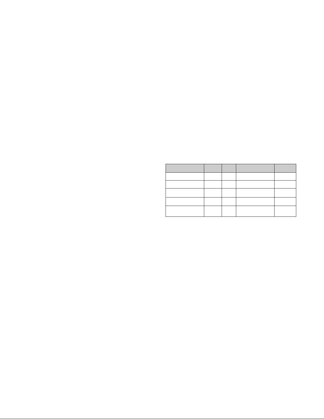
TIMING CHART
- 4 -
VIDEO
SYNC
B
D
C
F
E
A
<< Dot Clock (MHz), Horizontal Frequency (kHz), Vertical Frequency (Hz), Horizontal etc... (µs), Vertical etc... (ms) >>
H + 31.469 800 640 16 96 48
V – 70.8Hz 449 350 37 2 60
H – 31.469 840 640 16 96 48
V – 59.94 525 480 10 2 33
H – 37.5 840 640 16 64 120
V – 75 500 480 1 3 16
H – 31.468 900 720 18 108 54
V + 70.09 449 400 12 2 35
H + 37.879 1056 800 40 128 88
V + 60.317 628 600 1 4 23
H + 46.875 1056 800 16 80 160
V + 75.0 625 600 1 3 21
H+/– 49.725 1152 832 32 64 224
V+/– 74.55 667 624 1 3 39
H – 48.363 1344 1024 24 136 160
V – 60.0 806 768 3 6 29
H – 60.123 1312 1024 16 96 176
V – 75.029 800 768 1 3 28
H+/– 68.681 1456 1152 32 128 144
V+/– 75.062 915 870 3 3 39
H+/– 61.805 1504 1152 18 134 200
V+/– 65.96 937 900 2 4 31
H + 63.981 1688 1280 48 112 248
V + 60.02 1066 1024 1 3 38
H + 79.976 1688 1280 16 144 248
V + 75.035 1066 1024 1 3 38
Mode
H/V
Sort
1
2
3
4
5
6
7
8
9
10
11
12
13
25.175
28.321
25.175
31.5
40.0
49.5
57.283
65.0
78.75
100.0
92.978
108.0
135.0
640x350
70Hz
640x480
60Hz
640x480
75Hz
720x400
70Hz
800x600
60Hz
800x600
75Hz
832x624
75Hz
1024x768
60Hz
1024x768
75Hz
1152x870
75Hz
1152x900
65Hz
1280x1024
60Hz
1280x1024
75Hz
Sync
Polarity
Frequency
Dot
Clock
Total Period
(E)
Video Active Time
(A)
Sync Duration
(D)
Back Porch
(F)
Front Porch
(C)
Resolution
Page 5

- 5 -
FRONT VIEW
Front Control Panel
REAR VIEW
OPERATING INSTRUCTIONS
L1811S
See Front Control Panel
Power Connect
213 46 5
1. Power ON/OFF Button
Use this button to turn the monitor on or off.
2. Power Indicator
This indicator lights up green when the monitor
operates normally. If the display is in DPM(Energy
Saving)mode, this indicator color change to amber.
3. MENU Button
Use these button to enter or exit the On Screen Display.
4.
▼▲◀▶
Button
Use these buttons to choose or adjust items in the On
Screen Display.
5.
AUTO/
SELECT Button
Use this button to enter a selection in the On Screen Display.
6.
LIGHTVIEW Button
Use this button to enter a selection in the on screen
display.
D-Sub Signal
Connect
100
100
Bring up Contrast and Brightness
adjustment.
When adjusting your display settings,
always press the AUTO/SELECT button
before entering the On Screen
Display(OSD). This will automatically
adjust your display image to the ideal settings for the current
screen resolution size (display mode).
The best display mode is 1280x1024/60Hz.
This function optimizes the brightness, contrast or color
value to the surrounding conditions and settings and
enables you to enjoy the most suitable picture by
adjusting the surroundings (DAY/NIGHT/USER MODE).
•
TEXT: For viewing letters
•
MOVIE: For viewing movies
•
PHOTO: For viewing pictures or the photographs
•
USER MODE: This function memorizes the
manual adjustment -Brightness, Contrast and
Color value on the On Screen Display.
Page 6
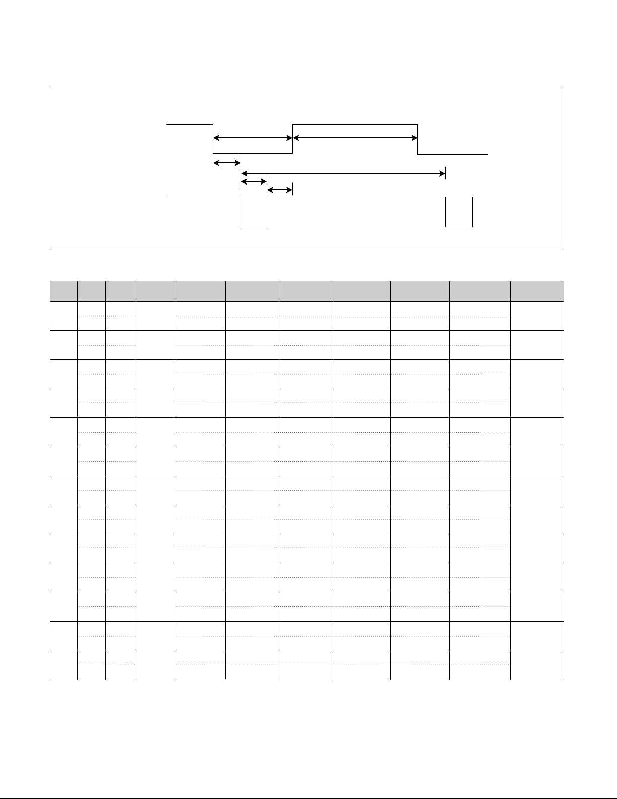
LCD MODULE
J702
J707
J709
P902
J706
CN1
CN2
CN3
CN4
CN7
CN6
CN5
Control PCB
Main PCB
Power PCB
- 6 -
WIRING DIAGRAM
Connector Ass’y P/N:
6631T20022E
Connector Ass’y P/N:
6631T20015R
Connector Ass’y P/N:
6631T25008Q
Connector Ass’y P/N:
6631T11012P
This function allows you to secure the current control settings, so that they cannot be inadvertently
changed. Press and hold the MENU button and button for 3 seconds: the message “CONTROLS
LOCKED” appears.
You can unlock the OSD controls at any time by pushing the MENU button and button for 3 seconds:
the message “CONTROLS UNLOCKED” will appear.
CONTROLS LOCKED/UNLOCKED
:
MENU and
OPERATING INSTRUCTIONS
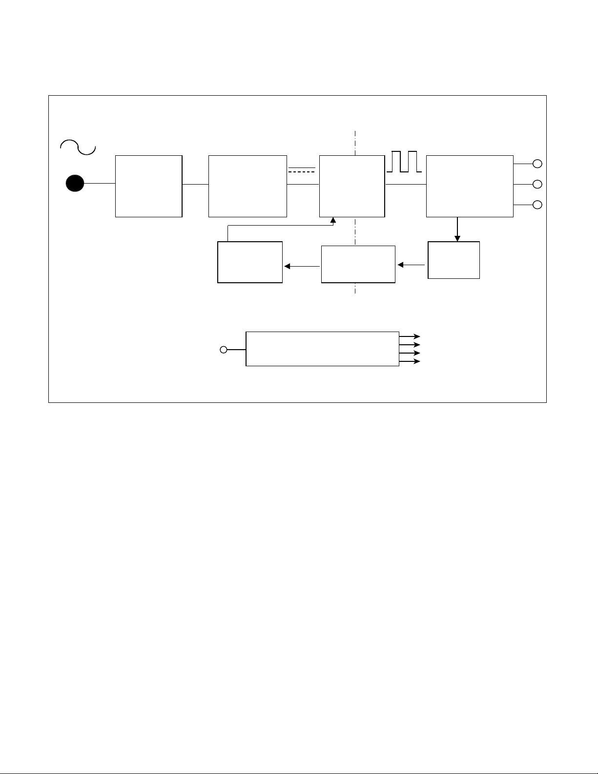
Page 7
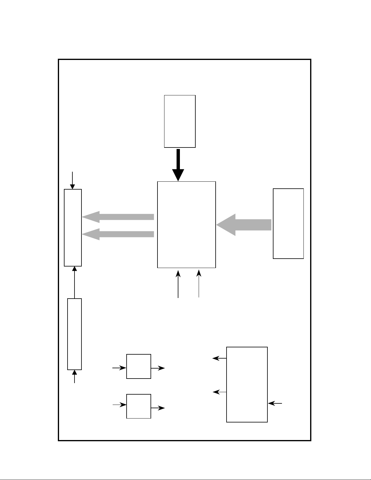
- 7 -
D-SUB
MST9111
including
(ADC/LVDS/SCALER )
MTV312
Micom
LCD Module
R,G,B
differential
LVDS
(Low Voltage
Differential
Signaling)
5V
3.3V
Reg.
2.5V
Reg.
5V
5V
12V
R,G,B, H/V Sync
Power
5V
AC Input
Inverter Output
Inverter
12V
3.3V
2.5V
3.3V
2.5V
BLOCK DIAGRAM
Page 8

- 8 -
DESCRIPTION OF BLOCK DIAGRAM
1. Video Controller Part & Display Data Transmitter Part.(MST9111)
This part amplifies the level of video signal for the digital conversion and
converts from the analog video signal to the digital video signal using a pixel clock.
The pixel clock for each mode is generated by the PLL.
The range of the pixel clock is from 25MHz to 135MHz.
This part consists of the Scaler.
The Scaler gets the video signal converted analog to digital,
interpolates input to 1280 x 1024 resolution signal and outputs 8-bit R, G, B signal to transmitter.
Especially pre-amp / ADC / Video controller/ Transmitter are merged to one chip “MST9111” by MSTAR.
This part transmit digital signal from the Scaler to the receiver of module.
2. Micom Part
This Part consists of EEPROM IC which stores control data, Reset IC and the Micom.
The Micom distinguishes polarity and frequency of the H/V Sync are supplied from signal cable.
The controlled data of each modes is stored in EEPROM.
3. Power Part
This part consists of the one 3.3V and one 2.5 regulators to convert power which is provided 5V in LIPS Board.
5V is provided for LCD Panel.
Also, 5V is converted 3.3V and 2.5V by regulator. Converted power is provided for IC in the main board.
4. Inverter
The inverter converts from DC12V to AC 700Vrms and operates back-light lamps of module.
Page 9
- 9 -
Power Board Block Diagram
EMI
COMPONENTS
LINE
100 ~ 240V
INPUT RECTIFIER
AND FILTER
ENERGY
TRANSFER
OUTPUT RECTIFIER
AND FILTER
12V
5V
GND
SIGNAL
COLLECT-
ION
PHOTO
INVERTER CIRCUIT
High Voltage output
12V
-COUPLER
ISOLATION
PWM CONTROL
CIRCUIT
HVDC
100KHz
PRIMARY SECONDARY
50 ~ 60Hz
Operation description_Power
1. EMI components.
This part contains of EMI components to comply with global marketing EMI standards like FCC, VCCI CISPR, the
circuit included a line-filter, across line capacitor and of course the primary protection fuse.
2. Input rectifier and filter.
This part function is for transfer the input AC voltage to a DC voltage through a bridge rectifier and a bulk capacitor.
3. Energy Transfer.
This part function is transfer the primary energy to secondary through a power transformer.
4. Output rectifier and filter.
This part function is to make a pulse width modulation control and to provide the driver signal to power switch, to
adjust the duty cycle during different AC input and output loading condition to achive the dc output stablize, and also
the over power protection is also monitor by this part.
5. Photo-Coupler isolation.
This part function is to feed back the dc output changing status through a photo transistor to primary controller to
achieve the stabilized dc output voltage.
6. Signal collection.
This part function is to collect the any change from the dc output and feed back to the primary through photo
transistor
Page 10

- 10 -
ADJUSTMENT
All adjustment are thoroughly checked and corrected when the monitor leaves the factory, but sometimes several minor
adjustment may be required.
Adjustment should be following procedure and after warming up for a minimum of 10 minutes.
• Alignment appliances and tools.
- IBM compatible PC
- Programmable Signal Generator.
(eg. VG-819 made by Astrodesign Co.)
- E(E)PROM with each mode data saved.
1. Adjustment process for LCD MONITOR
1) Display half window pattern(or mixed white and black pattern)at Mode 8 (1024x768@60Hz).
2) Press the POWER and MENU key at the same time to light monitor, then go to adjustment mode.
3) Press the MENU s/w, next press UP button, you will see adjustment OSD menu.
4) Press the AUTO/SELECT to select the adjustment item first(use the same button to exit)next do the operation to
the relative item.Ex) 17HYDIS is used at 17AU, press right button to select. Press the AUTO/SELECT then
selected proper Module.
5) Press down button to move the place of ADC CAL. Press the AUTO/SELECT to select, right button is pressed for
adjustment.
6) When adjustment is finished, press the POWER key twice to light monitor again. The dajustment ends.
2. Adjustment for EDID
1) Use this procedure only when there is some probelm on EDID data.
2) Connect the D-sub cable.
3) Select EDID → Write EDID[A0] command and Enter.
220
IBM
Compatible PC
Video Signal
Generator
PARALLEL PORT
Power inlet (required)
Power LED
ST Switch
Power Select Switch
(110V/220V)
Control Line
Not used
RS232C
PARALLEL
V-SYNC
POWER
ST
VGS
MONITOR
E
E
V-Sync On/Off Switch
(Switch must be ON.)
F
F
A
A
B
B
C
C
15
10
5
5
69
1
1
1
14
13
25
6
5V
5V
5V
4.7K
4.7K
4.7K
74LS06
74LS06
OFF ON
OFF
ON
11
Figure 1. Cable Connection
Page 11

- 11 -
TROUBLESHOOTING GUIDE
1. NO POWER
CHECK U803.
CHECK
U803 PIN 3
VOLTAGE
(5V) ?
NO
NO POWER
(POWER INDICATOR OFF)
CHECK POWER
BOARD, AND FIND
OUT A SHORT POINT
AS OPENING
EACH POWER LINE
CHECK J709
VOLTAGE
PIN5, PIN6 (5V)?
NO
CHECK 5VS LINE
(OPEN CHECK)
CHECK
U804 PIN 3 Voltage
(5V) ?
NO
CHECK IIC LINE
CONNECTION
(U501, U502)
CHECK U201 VCC,
XTAL, RESET
IS U201
PIN114 (3.3V)
VOLTAGE REPEATED
AS PULSE
SHAPE ?
NO
YES
YES
YES
NO PROBLEM
YES
CHECK KEY CONTROL
CONNECTOR ROUTINE
Page 12

- 12 -
2. NO RASTER (OSD IS NOT DISPLAYED) – LIPS
CHECK MICOM INV
ON/OFF PORT.
J707 PIN8
12V?
NO
NO RASTER
(OSD IS NOT DISPLAYED)
CHECK LIPS
J709
PIN5, PIN 6
5V?
NO
1. CONFIRM BRIGHTNESS
OSD CONTRL STATE.
2. CHECK MICOM DIM-ADJ
PORT
J707 PIN7
5V?
NO
LIPS
CHECK
PULSE AS
CONTACTING SCOPE
PROBE TO CAUTION LABEL.
(CONTACT PROBE TO
CAUTION LABEL.
CAN YOU SEE PULSE
AT YOUR
SCOPE?
NO
REPLACE CCFL LAMP
IN THE LCD MODULE
YES
YES
YES
YES
Page 13

- 13 -
1. CHECK PIN122, 123
SOLDERING CONDITION
2. CHECK X501
3. TROUBLE IN U201
U201
POWER PINS
3.3V?
NO
CHECK U804
U201
PIN122, 123
OSCILLATE AS
12MHZ?
CHECK CONNECTION LINE
FROM U201 TO U501
TROUBLE IN CABLE
OR LCD MODULE
YES
YES
YES
3. NO RASTER (OSD IS NOT DISPLAYED) – MST9111
NO RASTER
(OSD IS NOT DISPLAYED)
U501
PIN41 IS 64KHz H-SYNC?
PIN42 IS 60Hz V-SYNC?
IS PULSE APPEARED
AT SIGNAL PINS?
NO
NO
Page 14

- 14 -
4. TROUBLE IN DPM
TROUBLE IN DPM
TROUBLE IN PC
CHECK PC
PC IS NOT GOING
INTO DPM OFF MODE
NO
TROUBLE IN
X501
NO
TROUBLE IN
SIGNAL CABLE
NO
YES
YES
YES
CHECK
U501 PIN 11,12
WAVEFORM
(12MHz) ?
CHECK
R734, R741
(SYNC) ?
CHECK
U501 PIN 24
(0V) ?
Page 15

PRINTED CIRCUIT BOARD
- 15 -
1. MAIN BOARD (Component Side)
R711
R710
J708
R533
R534
R537
C516
J706
1
C
R552
Q507
R555
R553
Q508
C508
R556
R554
R766
C509
C
Q704
R709
R708R528
R580
R570
R747
R748
R560
C711
C710
C709
R529
R581
R571
R562
C708
1
J702
U502
R532
C550
R550
C514
R531
R530
R539
R559 R513
R557
R763
D719
R765R764
U703
R762
C501
Q503
R535
R542
Q502
5
40
C530
R745
R744
Q703
C507
R561
R558
Q509
U503
R727
R726
R724
R723
C712
U702
X501
C513C512
R536
10
15
C503
U501
35
ZD703
D707
C703 R725
R722
J703
P/N :6870T630A11
DATE :2003.02.24
R510
Q506
MODEL:L1811SL/L1810BL
C502
R504
R502
R501
20
25
30
C730
R520
R705
R741
R716
ZD711
ZD704
ZD701
R511
1
R525
R515
R509
Q504
C223
R596
R595
R590
R592
R591
R522
R540
R593
R538
C506
C505
C208
R219
R218
R523
R524
C731
R740
R733
R734
Q702
R707
R717
C707
ZD702
C822
C820
C231
C240
C232
C206
C205
C204
R551
A
70
C220
R541
R240
R209
R208
R203
R202
R201
Q505
60
C218
C224
40 50
C215
C210
C209
C207
C744C743
Q701
D702
R703R701
U802
C821
R812
C803
C804
C244
C245
C248
C249
C246
C250
C247
C233
80
C227
C222
R212
R217
R216
R213
R211
R215
R214
R210
20
30
C216
C742C741
R758
D718 D706 D701
R706
C740
R811
90
100
C221
C217
10
R207
A
C735C734
C714
ZD706
R759
R761
D717
D716
J709
1
J705
C819
C818
R753
110
C219
C226
C230
C214
C228
C229
C225
U201
1
R205
R204
R729
C713
ZD709
R730
R767
Q706
ZD705
R731
1
C727
Q705
R751
C817
X201
C831
C716
R728
C739
R768
Q707
D715
B
C810
R813
R735
C809
R750
C832
C760
R803
C801
C715
C738C737
R771
R770
R769
D714
D711
D709
D708
C732
R849 R845
R844
R843R840
R841
R814
U805
C802
C829
C828
C733
R774
R773
R772
J701
D713
D712 D710
B
R848
R847 R846
R842
J707
1
U804
U803
C705
C704
R754
R732
R755
C706
ZD707
ZD708
R757
R756
Page 16

- 16 -
2. POWER B
OARD (Component Side)
3. POWER B
OARD (Solder Side)
4. CONTROL B
OARD
SW8
POWER
A
G
LED1
SW7
SET/AUTO
R3
RIGHT
SW5 SW6
R5
LEFT
R4R7R6
R8
SW4
UP
SW3
DOWNMENU
SW2SW1
INPUT
C2
C1
R1
R2
J1
Page 17

- 17 -
1
13
11
10
6
5
4
c
12
a
a
b
3
9
8
2
7
EXPLODED VIEW
Page 18

- 18 -
EXPLODED VIEW PARTS LIST
Ref. No.
1
2
3
4
5
6
7
8
9
10
11
12
13
a
b
c
Part No.
3091TKL044P
6304FLP034A
or 6304FLP044A
3809TKL025L
3043TKK091E
6871TST389A
6631T11012P
6633TZA008C
4951TKS078X
6871TMT414A
6871TPT225A
4814TKK187A
4950TKK429A
6850TD9004D
or 6850TD9004A
1SZZTER001H
332-113S
332-105G
Description
CABINET ASSEMBLY, L1811SL BRAND , ANALOG ONLY
LCD(LIQUID CRYSTAL DISPLAY), LM181E06-A4M1 LG PHILPS TFT COLOR SXGA 18.1" LVDS SMM
LCD(LIQUID CRYSTAL DISPLAY), LM181E06-A4C3 LG PHILPS TFT COLOR SXGA LVDS SMM
BACK COVER ASSEMBLY, LB801G , L1811SG (ANALOG ONLY)
TILT SWIVEL ASSEMBLYLM805L -HIPS NO USB
PWB(PCB) ASSEMBLY,SUB, L1811SL L1810BL CONTROL TOTAL BRAND CONTROL
CONNECTOR ASSEMBLY, 30P H-H 100MM UL20276 PANEL LINK LB886F
INVERTER ASSEMBLY, ALPS KUBNKM045A 6-LAMPS,18" DELL
METAL ASSEMBLY, "FRAME MAIN, L1810BL/L1811SL
PWB(PCB) ASSEMBLY,MAIN, L1811SL ALRDR BRAND CL-43 TOTAL
PWB(PCB) ASSEMBLY,POWER, LB800H POWER TOTAL BRAND
SHIELD REAR LB886F
METAL REAR LB800H
CABLE, D-SUB, UL20276-9C(5.8MM) DT 1560MM GRAY(85964) LB500L DM
CABLE, D-SUB, UL20276-9C(5.8MM) DT 1870MM GRAY(85964) LB500K DM
DRAWING, D3.0 L10.0 MSWR/BK .
SCREW, DRAWING, D3.0 L12.0 MSWR/BK .
SCREW, DRAWING, PVS+4*10(MSWR/BK)
Page 19

- 19 -
DATE: 2003. 3. 8.
*S *AL LOC. NO. PART NO. DESCRIPTION / SPECIFICATION
C204 0CK104CK56A 0.1UF 1608 50V 10% R/TP X7R
C205 0CK104CK56A 0.1UF 1608 50V 10% R/TP X7R
C206 0CK104CK56A 0.1UF 1608 50V 10% R/TP X7R
C207 0CK104CK56A 0.1UF 1608 50V 10% R/TP X7R
C208 0CK104CK56A 0.1UF 1608 50V 10% R/TP X7R
C209 0CK104CK56A 0.1UF 1608 50V 10% R/TP X7R
C210 0CK104CK56A 0.1UF 1608 50V 10% R/TP X7R
C214 0CK104CK56A 0.1UF 1608 50V 10% R/TP X7R
C215 0CK104CK56A 0.1UF 1608 50V 10% R/TP X7R
C216 0CK104CK56A 0.1UF 1608 50V 10% R/TP X7R
C217 0CK104CK56A 0.1UF 1608 50V 10% R/TP X7R
C218 0CK104CK56A 0.1UF 1608 50V 10% R/TP X7R
C219 0CK104CK56A 0.1UF 1608 50V 10% R/TP X7R
C220 0CK104CK56A 0.1UF 1608 50V 10% R/TP X7R
C221 0CK104CK56A 0.1UF 1608 50V 10% R/TP X7R
C222 0CK104CK56A 0.1UF 1608 50V 10% R/TP X7R
C223 0CK104CK56A 0.1UF 1608 50V 10% R/TP X7R
C224 0CK104CK56A 0.1UF 1608 50V 10% R/TP X7R
C225 0CK104CK56A 0.1UF 1608 50V 10% R/TP X7R
C226 0CK104CK56A 0.1UF 1608 50V 10% R/TP X7R
C227 0CK104CK56A 0.1UF 1608 50V 10% R/TP X7R
C230 0CK104CK56A 0.1UF 1608 50V 10% R/TP X7R
C231 0CK104CK56A 0.1UF 1608 50V 10% R/TP X7R
C232 0CK104CK56A 0.1UF 1608 50V 10% R/TP X7R
C233 0CK104CK56A 0.1UF 1608 50V 10% R/TP X7R
C240 0CK104CK56A 0.1UF 1608 50V 10% R/TP X7R
C501 0CK104CK56A 0.1UF 1608 50V 10% R/TP X7R
C502 0CC101CK41A 100PF 1608 50V 5% R/TP NP0
C503 0CC101CK41A 100PF 1608 50V 5% R/TP NP0
C505 0CC101CK41A 100PF 1608 50V 5% R/TP NP0
C506 0CC101CK41A 100PF 1608 50V 5% R/TP NP0
C512 0CC180CK41A 18PF 1608 50V 5% R/TP NP0
C513 0CC030CK01A 3PF 1608 50V 0.25 PF R/TP NP0
C514 0CH8106F611 10UF 16V M 85STD(CYL) R/TP
C516 0CK104CK56A 0.1UF 1608 50V 10% R/TP X7R
C703 0CK104CK56A 0.1UF 1608 50V 10% R/TP X7R
C707 0CC680CK41A 68PF 1608 50V 5% R/TP NP0
C708 0CK103CK51A 0.01UF 1608 50V 10% R/TP B(Y5
C709 0CK103CK51A 0.01UF 1608 50V 10% R/TP B(Y5
C710 0CK103CK51A 0.01UF 1608 50V 10% R/TP B(Y5
C711 0CK103CK51A 0.01UF 1608 50V 10% R/TP B(Y5
C727 0CK105CD56A 1UF 1608 10V 10% R/TP X7R
C730 0CC101CK41A 100PF 1608 50V 5% R/TP NP0
C731 0CC680CK41A 68PF 1608 50V 5% R/TP NP0
C732 0CK103CK51A 0.01UF 1608 50V 10% R/TP B(Y5
C740 0CE477EH618 470UF KMG 25V M FL TP 5
C742 0CK104CK56A 0.1UF 1608 50V 10% R/TP X7R
C743 0CK104CK56A 0.1UF 1608 50V 10% R/TP X7R
C744 0CK104CK56A 0.1UF 1608 50V 10% R/TP X7R
C760 0CE107EF610 “100UF KMG,RD 16V 20% FL BULK”
C801 0CK103CK51A 0.01UF 1608 50V 10% R/TP B(Y5
C802 0CK104CK56A 0.1UF 1608 50V 10% R/TP X7R
DATE: 2003. 3. 8.
*S *AL LOC. NO. PART NO. DESCRIPTION / SPECIFICATION
C803 0CK105CD56A 1UF 1608 10V 10% R/TP X7R
C804 0CC102CK41A 1000PF 1608 50V 5% R/TP NP0
C809 0CK105CD56A 1UF 1608 10V 10% R/TP X7R
C810 0CC102CK41A 1000PF 1608 50V 5% R/TP NP0
C817 0CE107EF610 “100UF KMG,RD 16V 20% FL BULK”
C818 0CK104CK56A 0.1UF 1608 50V 10% R/TP X7R
C819 0CK103CK51A 0.01UF 1608 50V 10% R/TP B(Y5
C820 0CE107EF610 “100UF KMG,RD 16V 20% FL BULK”
C821 0CK103CK51A 0.01UF 1608 50V 10% R/TP B(Y5
C822 0CK104CK56A 0.1UF 1608 50V 10% R/TP X7R
C828 0CK104CK56A 0.1UF 1608 50V 10% R/TP X7R
C829 0CK103CK51A 0.01UF 1608 50V 10% R/TP B(Y5
C831 0CE107EF610 “100UF KMG,RD 16V 20% FL BULK”
C832 0CE107EF610 “100UF KMG,RD 16V 20% FL BULK”
D701 0DS226009AA KDS226 TP KEC SOT-23 80V 300
D702 0DS226009AA KDS226 TP KEC SOT-23 80V 300
D706 0DS226009AA KDS226 TP KEC SOT-23 80V 300
D707 0DD184009AA KDS184 TP KEC - 85V - - - 300
ZD701 0DZ560009GB BZT52C5V6S DIODES R/TP SOD323
ZD702 0DZ560009GB BZT52C5V6S DIODES R/TP SOD323
ZD703 0DZ560009GB BZT52C5V6S DIODES R/TP SOD323
ZD704 0DZ560009GB BZT52C5V6S DIODES R/TP SOD323
ZD711 0DZ560009GB BZT52C5V6S DIODES R/TP SOD323
U201 0IPRPM3004A MST9111 ANALOG MSTAR 128 LQFP
U501 0IZZTSZ257B MYSON 44P PLCC ST OTP L1710SL
U502 0ISG240860B M24C08W6 SGS-THOMSON 8SOP R/T
U702 0ICS240213A CAT24WC02J-TE13 8P SOP TP 2K
U802 0TFVI80036A SI3861DV VISHAY R/TP TSOP-6 4
U803 0IPMGNS001D LM1117MPX-2.5 NATIONAL SEMICO
U804 0IPMGNS001E LM1117MPX-3.3 NATIONAL SEMICO
U805 0TFVI80036A SI3861DV VISHAY R/TP TSOP-6 4
Q502 0TR390409AE FAIRCHILD KST3904(LGEMTF) TP
Q503 0IKE704200H KIA7042AP TO-92 TP 4.2 VOLT.
Q504 0TR390409AE FAIRCHILD KST3904(LGEMTF) TP
Q505 0TR390409AE FAIRCHILD KST3904(LGEMTF) TP
Q506 0TR390409AE FAIRCHILD KST3904(LGEMTF) TP
Q701 0TR390409AE FAIRCHILD KST3904(LGEMTF) TP
Q702 0TR390409AE FAIRCHILD KST3904(LGEMTF) TP
Q703 0TR390609FA KST3906-MTF TP SAMSUNG SOT23
Q704 0TR390609FA KST3906-MTF TP SAMSUNG SOT23
Q705 0TR390409AE FAIRCHILD KST3904(LGEMTF) TP
R201 0RJ0682D677 68 OHM 1/10 W 5% 1608 R/TP
REPLACEMENT PARTS LIST
CAUTION: BEFORE REPLACING ANY OF THESE COMPONENTS,
READ CAREFULLY THE SAFETY PRECAUTIONS IN THIS MANUAL.
* NOTE : S SAFETY Mark
AL ALTERNATIVE PARTS
MAIN BOARD
CAPACITORS
DIODEs
ICs
TRANSISTOR
RESISTORs
Page 20

DATE: 2003. 3. 8.
*S *AL LOC. NO. PART NO. DESCRIPTION / SPECIFICATION
R202 0RJ0682D677 68 OHM 1/10 W 5% 1608 R/TP
R203 0RJ0682D677 68 OHM 1/10 W 5% 1608 R/TP
R204 0RJ1002D677 10K OHM 1/10 W 5% 1608 R/TP
R205 0RJ1002D677 10K OHM 1/10 W 5% 1608 R/TP
R207 0RJ4700D677 470 OHM 1/10 W 5% 1608 R/TP
R208 0RJ0682D677 68 OHM 1/10 W 5% 1608 R/TP
R209 0RJ0682D677 68 OHM 1/10 W 5% 1608 R/TP
R210 0RJ0682D677 68 OHM 1/10 W 5% 1608 R/TP
R240 0RJ0682D677 68 OHM 1/10 W 5% 1608 R/TP
R501 0RJ4701D677 4.7K OHM 1/10 W 5% 1608 R/TP
R502 0RJ4701D677 4.7K OHM 1/10 W 5% 1608 R/TP
R504 0RJ4701D677 4.7K OHM 1/10 W 5% 1608 R/TP
R509 0RJ4701D677 4.7K OHM 1/10 W 5% 1608 R/TP
R510 0RJ4700D677 470 OHM 1/10 W 5% 1608 R/TP
R511 0RJ4700D677 470 OHM 1/10 W 5% 1608 R/TP
R513 0RJ0000D677 0 OHM 1/10 W 5% 1608 R/TP
R515 0RJ1002D677 10K OHM 1/10 W 5% 1608 R/TP
R520 0RJ4701D677 4.7K OHM 1/10 W 5% 1608 R/TP
R522 0RJ1000D677 100 OHM 1/10 W 5% 1608 R/TP
R523 0RJ0332D677 33 OHM 1/10 W 5% 1608 R/TP
R524 0RJ0332D677 33 OHM 1/10 W 5% 1608 R/TP
R525 0RJ1002D677 10K OHM 1/10 W 5% 1608 R/TP
R528 0RJ1000D677 100 OHM 1/10 W 5% 1608 R/TP
R529 0RJ1000D677 100 OHM 1/10 W 5% 1608 R/TP
R530 0RJ1000D677 100 OHM 1/10 W 5% 1608 R/TP
R531 0RJ1000D677 100 OHM 1/10 W 5% 1608 R/TP
R532 0RJ3301D677 3.3K OHM 1/10 W 5% 1608 R/TP
R533 0RJ0332D677 33 OHM 1/10 W 5% 1608 R/TP
R534 0RJ0332D677 33 OHM 1/10 W 5% 1608 R/TP
R535 0RJ3301D677 3.3K OHM 1/10 W 5% 1608 R/TP
R537 0RJ4701D677 4.7K OHM 1/10 W 5% 1608 R/TP
R538 0RJ4701D677 4.7K OHM 1/10 W 5% 1608 R/TP
R539 0RJ0000D677 0 OHM 1/10 W 5% 1608 R/TP
R540 0RJ1002D677 10K OHM 1/10 W 5% 1608 R/TP
R541 0RJ4701D677 4.7K OHM 1/10 W 5% 1608 R/TP
R542 0RJ1500D677 150 OHM 1/10 W 5% 1608 R/TP
R551 0RJ4702D677 47000 OHM 1/10 W 5% 1608 R/TP
R560 0RJ4701D677 4.7K OHM 1/10 W 5% 1608 R/TP
R562 0RJ4700D677 470 OHM 1/10 W 5% 1608 R/TP
R571 0RJ1000D677 100 OHM 1/10 W 5% 1608 R/TP
R580 0RJ1001D677 1K OHM 1/10 W 5% 1608 R/TP
R590 0RJ1000D677 100 OHM 1/10 W 5% 1608 R/TP
R591 0RJ1000D677 100 OHM 1/10 W 5% 1608 R/TP
R592 0RJ1000D677 100 OHM 1/10 W 5% 1608 R/TP
R593 0RJ1000D677 100 OHM 1/10 W 5% 1608 R/TP
R595 0RJ1000D677 100 OHM 1/10 W 5% 1608 R/TP
R596 0RJ4701D677 4.7K OHM 1/10 W 5% 1608 R/TP
R701 0RJ0752D677 75 OHM 1/10 W 5% 1608 R/TP
R703 0RJ0752D677 75 OHM 1/10 W 5% 1608 R/TP
R705 0RJ1000D677 100 OHM 1/10 W 5% 1608 R/TP
R706 0RJ0752D677 75 OHM 1/10 W 5% 1608 R/TP
R707 0RJ0682D677 68 OHM 1/10 W 5% 1608 R/TP
R708 0RJ4700D677 470 OHM 1/10 W 5% 1608 R/TP
R709 0RJ4700D677 470 OHM 1/10 W 5% 1608 R/TP
R716 0RJ4701D677 4.7K OHM 1/10 W 5% 1608 R/TP
R717 0RJ4701D677 4.7K OHM 1/10 W 5% 1608 R/TP
R722 0RJ1000D677 100 OHM 1/10 W 5% 1608 R/TP
R723 0RJ0332D677 33 OHM 1/10 W 5% 1608 R/TP
R724 0RJ0332D677 33 OHM 1/10 W 5% 1608 R/TP
R725 0RJ4701D677 4.7K OHM 1/10 W 5% 1608 R/TP
R726 0RJ1002D677 10K OHM 1/10 W 5% 1608 R/TP
R727 0RJ1002D677 10K OHM 1/10 W 5% 1608 R/TP
DATE: 2003. 3. 8.
*S *AL LOC. NO. PART NO. DESCRIPTION / SPECIFICATION
R733 0RJ1001D677 1K OHM 1/10 W 5% 1608 R/TP
R734 0RJ4701D677 4.7K OHM 1/10 W 5% 1608 R/TP
R735 0RJ0000D677 0 OHM 1/10 W 5% 1608 R/TP
R740 0RJ1001D677 1K OHM 1/10 W 5% 1608 R/TP
R741 0RJ4701D677 4.7K OHM 1/10 W 5% 1608 R/TP
R744 0RJ4701D677 4.7K OHM 1/10 W 5% 1608 R/TP
R745 0RJ4701D677 4.7K OHM 1/10 W 5% 1608 R/TP
R747 0RJ4701D677 4.7K OHM 1/10 W 5% 1608 R/TP
R748 0RJ4701D677 4.7K OHM 1/10 W 5% 1608 R/TP
R750 0RJ1001D677 1K OHM 1/10 W 5% 1608 R/TP
R751 0RJ1001D677 1K OHM 1/10 W 5% 1608 R/TP
R753 0RJ1001D677 1K OHM 1/10 W 5% 1608 R/TP
R803 0RJ0000D677 0 OHM 1/10 W 5% 1608 R/TP
R811 0RJ2202D677 22K OHM 1/10 W 5% 1608 R/TP
R812 0RJ5600D677 560 OHM 1/10 W 5% 1608 R/TP
R813 0RJ2202D677 22K OHM 1/10 W 5% 1608 R/TP
R814 0RJ5600D677 560 OHM 1/10 W 5% 1608 R/TP
R840 0RJ0332D677 33 OHM 1/10 W 5% 1608 R/TP
R841 0RJ0332D677 33 OHM 1/10 W 5% 1608 R/TP
R842 0RJ0332D677 33 OHM 1/10 W 5% 1608 R/TP
R843 0RJ0332D677 33 OHM 1/10 W 5% 1608 R/TP
R844 0RJ0332D677 33 OHM 1/10 W 5% 1608 R/TP
R845 0RJ0332D677 33 OHM 1/10 W 5% 1608 R/TP
R846 0RJ0332D677 33 OHM 1/10 W 5% 1608 R/TP
R847 0RJ0332D677 33 OHM 1/10 W 5% 1608 R/TP
R848 0RJ0332D677 33 OHM 1/10 W 5% 1608 R/TP
R849 0RJ0332D677 33 OHM 1/10 W 5% 1608 R/TP
X501 6212AA2004A HC-49U TXC 12.0MHZ +/- 30 PPM
BD901 0DD360000DA D3SBA60 BK SHINDENGEN 600V
C901 0CBZTBU002B BULK PCX2 335 474K
C902 0CKZTBU006B NK E 332M 250V BK10.0 DA2GYE3
C903 0CKZTBU006B NK E 332M 250V BK10.0 DA2GYE3
C904 0CBZTBU002A BULK PCX2 335 224K
C905 0CZZTAB002C KMF 18*40 SYE / SWE 400V 120U
C906 0CK10302945 0.01UF 2KV Z F TR
C907 0CE476EK638 47UF KMG 50V M FM5 TP 5
C908 0CQ2721N419 2700PF 100V J PE NI TP
C909 0CK1020K515 1000PF 50V K B TR
C911 0CE228EF630 2200UF KMG 16V M FM5 BULK
C913 0CE108BF630 1000UF KME 16V M FM5 BULK
C914 0CE228ED630 “2200UF KMG,RD 10V 20% BULK FM”
C915 0CE228ED630 “2200UF KMG,RD 10V 20% BULK FM”
C916 181-288L MKT 100V 823JTR PHS26823
C918 0CE228ED630 “2200UF KMG,RD 10V 20% BULK FM”
C919 0CKZTBU006B NK E 332M 250V BK10.0 DA2GYE3
C921 0CE228EF630 2200UF KMG 16V M FM5 BULK
C922 0CKZTTA002E EKR3A102K09FK5 SAMWHA 1KV 100
C923 0CKZTTA002E EKR3A102K09FK5 SAMWHA 1KV 100
C924 0CE336BH638 33UF KME 25V M FM5 TP5
D901 0DD400709CB UF4007 TP G.I DO204AL 1000V
D902 0DR400409AB UF4004 TP G.I DO204AL 400V 1A
D903 0DRIR00011B 16CTQ100 I.R ST TO220 100V 16
D906 0DRIR00021A 30CTQ060 I.R ST TO220 60V 30A
D907 0DS113309AA 1SS133 TP ROHM KOREA DO34 90V
F901 0FZZTTH001D “TIME LAG HBC 3.15A/250V,215 3”
FH1 430-858C AFC-520 BAE EUN TA
- 20 -
OTHERs
POWER BOARD
Page 21

DATE: 2003. 3. 8.
*S *AL LOC. NO. PART NO. DESCRIPTION / SPECIFICATION
FH2 430-858C AFC-520 BAE EUN TA
IC901 0IPMGIH001A “ICE2AS01 INFINEON 8P,DIP ST O”
IC904 0ISS431000A KA431AZ (LM431AZ)
IC905 0ISS780500F KA7805
L901 150-A85F “LX31 GET BAR CHOKE,3.3UH,LB88”
L902 150-A85F “LX31 GET BAR CHOKE,3.3UH,LB88”
LF901 6200TZZ001A “- GO BK L/FILTER,9MH,LB886F”
LF902 6200TZZ001A “- GO BK L/FILTER,9MH,LB886F”
P901 6620TKB002A BAE EUN AC UNIVERSAL 3PIN BLA
PC1 0ILI817000E LTV-817M-V(B) 4P BK PHOTO CO
Q902 0TFFN10004A INFINEON SPP11N60C2 ST TO220
R901 0RD6803A609 680K OHM 1/2 W (7.0) 5% TA52
R902 0RD3902A609 39K OHM 1/2 W (7.0) 5% TA52
R903 0RD3902A609 39K OHM 1/2 W (7.0) 5% TA52
R906A 0RX5102J609 51KOHM 1 W 5% TA52
R906B 0RX5102J609 51KOHM 1 W 5% TA52
R907 0RD0102Q609 10 1/4W(3 5% TA52
R908 0RD0222Q609 22 1/4W(3 5% TA52
R909 0RD1001Q609 1K 1/4W(3 5% TA52
R910 0RD0431A609 4.3 OHM 1/2 W (7.0) 5% TA52
R911 0RD1004A609 1.0M OHM 1/2 W (7.0) 5% TA52
R912 0RD1004A609 1.0M OHM 1/2 W (7.0) 5% TA52
R913 0RN1102F409 11K 1/6W 1% TA52
R914 0RD1002Q609 10K 1/4W(3 5% TA52
R917 0RD1201Q609 1.20K 1/4W(3 5% TA52
R918 0RD1000Q609 100 1/4W(3 5% TA52
R920 0RN4702F409 47K 1/6W 1% TA52
R921 0RN2701F409 2.7K OHM 1/6 W 1.00% TA52
R923 0RB0330K607 0.33 OHM 2 W 5% TA62
R924 0RD0752Q609 75 1/4W(3 5% TA52
R925 0RD1002Q609 10K 1/4W(3 5% TA52
R926 0RN0471H609 4.7 OHM 1/2 W 5% TA52
R927 0RD0102A609 10 OHM 1/2 W (7.0) 5% TA52
R928 0RD0202Q609 20 1/4W(3 5% TA52
T901 6170TMZ125B EER3016 340UH V-10PIN LB886F
TH901 971-0054 TIN 50MM TAPING
TH902 6322TA080AA TP8D13 DAEWOO +/- 15% 110/22
ZD901 0DZ470009BC GDZ4.7B TP GRANDE DO34 0.5W 4
LED1 0DLLT0208AA LITEON LTST-C155KGJSKT R/TP G
R1 0RJ4701D677 4.7K OHM 1/10 W 5% 1608 R/TP
R2 0RJ4701D677 4.7K OHM 1/10 W 5% 1608 R/TP
R3 0RJ8200D677 820 OHM 1/10 W 5% 1608 R/TP
R4 0RJ8200D677 820 OHM 1/10 W 5% 1608 R/TP
R5 0RJ1501D677 1.5K OHM 1/10 W 5% 1608 R/TP
R6 0RJ1501D677 1.5K OHM 1/10 W 5% 1608 R/TP
R7 0RJ2201D677 2200 OHM 1/10 W 5% 1608 R/TP
R8 0RJ2201D677 2200 OHM 1/10 W 5% 1608 R/TP
SW1 140-058E SKHV10910B LGEC NON 12V 20A H
SW2 140-058E SKHV10910B LGEC NON 12V 20A H
SW3 140-058E SKHV10910B LGEC NON 12V 20A H
SW4 140-058E SKHV10910B LGEC NON 12V 20A H
SW5 140-058E SKHV10910B LGEC NON 12V 20A H
SW6 140-058E SKHV10910B LGEC NON 12V 20A H
SW7 140-058E SKHV10910B LGEC NON 12V 20A H
SW8 140-058E SKHV10910B LGEC NON 12V 20A H
- 21 -
CONTROL BOARD
Page 22

PIN CONFIGURATION
- 22 -
MST9111 DUAL MSTAR 128P
1
2
3
4
5
6
7
8
9
10
11
12
13
14
15
16
17
18
19
20
21
22
23
24
25
26
27
28
29
30
31
32
33
34
35
36
37
38
128
127
126
125
124
123
122
121
120
119
118
117
116
115
114
113
112
111
110
109
108
107
106
105
104
103
NC
VSYNC0
HSYNC0
AVSS_PLL
AVDD_PLL
XOUT
XIN
HWRESETZ
DDCROM_DAT
DDCROM_CLK
DDC1_CLK
DDC1_DAT
NCNCVDDP
GNDP
GNDC
VDDCNCNCNCVDDP
GNDPNCNC
BYPASS
39404142434445464748495051525354555657585960616263
64
102
101
100
99
98
97
96
95
94
93
92
91
90
89
88
87
86
85
84
83
82
81
80
79
78
77
76
75
74
73
72
71
70
69
68
67
66
65
NC
AVSS
NC
NC
AVSS
NC
NC
AVDD
NC
NC
AVSS
NC
NC
AVDD
REXT
AVDD_PLL
AVSS_PLL
AVDD
AVSS
NC
NC
NC
NC
NC
NC
NC
BIN0M
BIN0
GIN0M
GIN0
SOGIN0
RIN0M
RIN0
AVSS
AVDD
RMID
REFP
REFM
AVSS_PLL
NC
NC
NC
NC
LVB0M
LVB0P
GNDP
VDDP
LVB1M
LVB1P
LVB2M
LVB2P
LVBCKM
LVBCKP
LVB3M
LVB3P
VDDC
GNDC
GNDP
VDDP
LVA0M
LVA0P
LVA1M
LVA1P
LVA2M
LVA2P
LVACKM
LVACKP
GNDP
VDDP
LVA3M
LVA3P
NC
NC
NC
NC
NC
AVSS
CSZ
SDA
SCL
INT
PWM0
PWM1
NCNCNCNCNCNCNCNCNC
VDDP
GNDP
GNDC
VDDC
NC
NC
VDDP
GNDP
GNDC
VDDC
MST9111
VC646960210F
Pin 1
PIN DIAGRAM
Page 23

- 23 -
CAT24WC08J-TE13 8P
A
0
A
1
A
2
V
SS
V
CC
WP
SCL
SDA
A
0
A
1
A
2
V
SS
V
CC
WP
SCL
SDA
1
2
3
4
8
7
6
5
1
2
3
4
8
7
6
5
A
0
A
1
A
2
V
SS
V
CC
WP
SCL
SDA
1
2
3
4
8
7
6
5
PIN CONFIGURATION
DIP Package(p) SOIX Package(J)
TSSOP Package(U)
BLOCK DIAGRAM
PIN FUNCTION
Pin Name
A0, A1, A2
SDA
SCL
WP
Vcc
Vss
Function
Device Adress Inputs
Serial Data/Address
Serial Clock
Write Protect
+1.8V to + 6.0V power Supply
Ground
EXTERNAL LOAD
V
V
SDA
WP
SCL
CC
SS
D
OUT
ACK
WORD ADDRESS
BUFFERS
START/STOP
LOGIC
XDEC
CONTROL
LOGIC
STATE COUNTERS
A
0
A
1
A
2
SLAVE
ADDRESS
COMPARATORS
SENSE AMPS
SHIFT REGISTERS
COLUMN
DECODERS
2
E PROM
DATA IN STORAGE
HIGH VOLTAGE/
TIMING CONTROL
Page 24

SCHEMATIC DIAGRAM
- 24 -
1. SCALER
Page 25

- 25 -
2. MICOM
Page 26

- 26 -
3. POWER
Page 27

- 27 -
4. CONNECTOR/JACKS
Page 28

- 28 -
5. KEY PART
Page 29

- 29 -
6. POWER
Page 30

Mar. 2003
P/NO : 3828TSL082L Printed in Korea
 Loading...