

Page 1
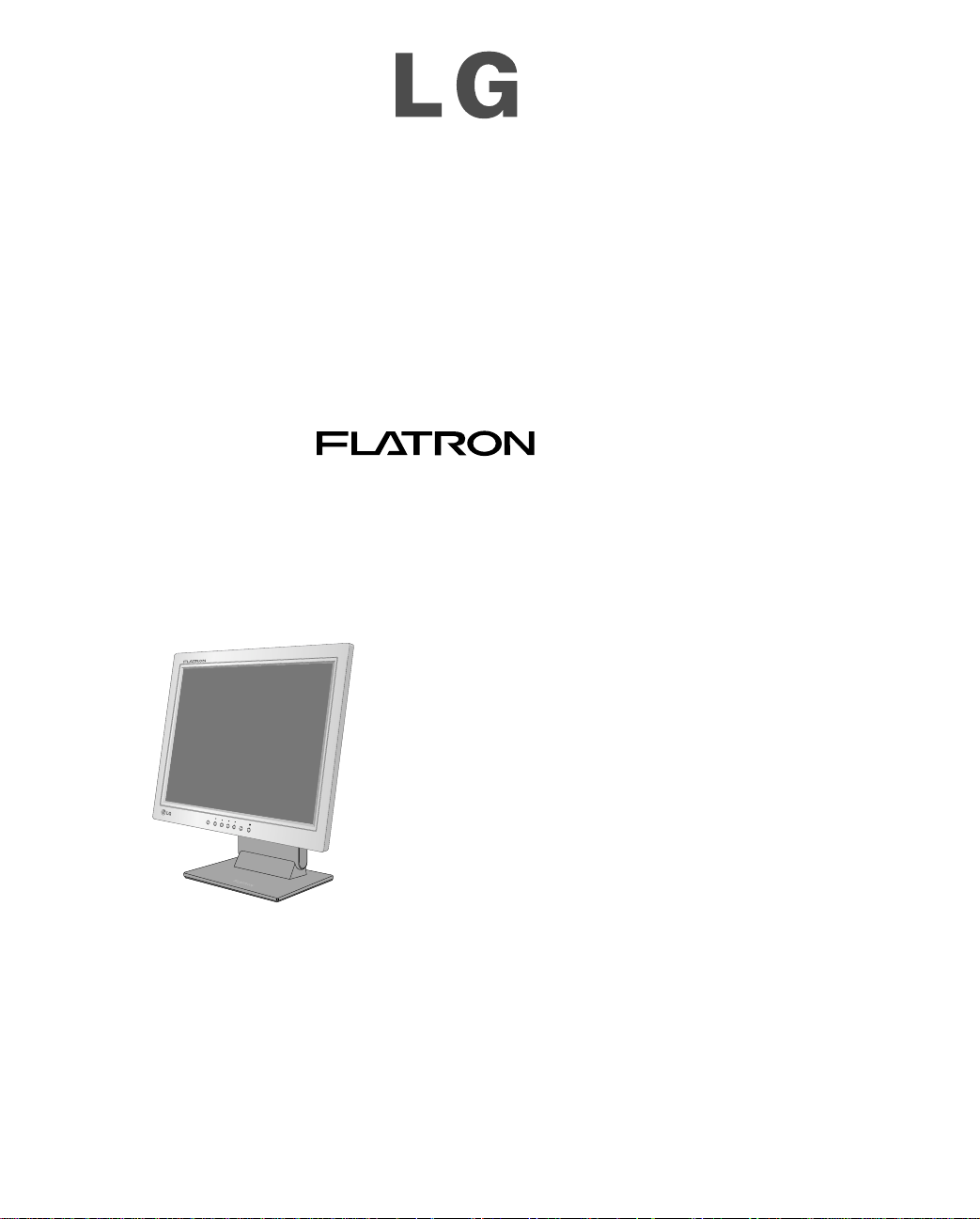
COLOR MONIT OR
SER VICE MANUAL
CHASSIS NO. : CL-32
F ACTORY MODEL: L1510SFK
MODEL: L1510SF (LB500K-VL)
CAUTION
BEFORE SERVICING THE UNIT,
READ THE SAFETY PRECAUTIONS IN THIS MANUAL.
L1510SF
MENU
A
U
TO/
SE
LECT
Page 2
CONTENTS
SPECIFICATIONS
- 2 -
1. LCD CHARACTERISTICS
Type : TFT XGA LCD Module
Size : 352.0(H) x 263.5(V) x 14.0(T)
Pixel Pitch : 0.297mm x 0.297mm
Color Depth :
6bits(with FRC)/ 16M colors
Active Video Area : 15.0inch
(304.128 x 228.096)
Surface Treatment : Anti-Glare, Hard Coating (3H)
Backlight Unit : Top/Bottom edge side 2CCFL
Electrical Interface : LVDS interface
2. OPTICAL CHARACTERISTICS
2-1. Viewing Angle by Contrast Ratio
≥
10
Left : 55° min. Right : 55° min.
Top : 40° min. Bottom : 40° min.
2-2. Luminance
:
160(min.), 200(typ.) at Center point
2-3. Contrast Ratio :250(min.), 350(typ.)
3. SIGNAL (Refer to the Timing Chart)
3-1. Sync Signal
1) Type : Separate Sync. (Horizontal & Vertical)
2) Input Voltage Level: Low=0~0.8V, High=2.1~5.5V
3) Sync Polarity : Positive or Negative
3-2. Video Input Signal
1) Type : R, G, B Analog
2) Voltage Level : 0~0.714 V
a) Color 0, 0 : 0 Vp-p
b) Color 7, 0 : 0.467 Vp-p
c) Color 15, 0 : 0.714 Vp-p
3) Input Impedance : 75 Ω
3-3. Operating Frequency
Horizontal : 30 ~ 63kHz
Vertical : 56 ~ 75Hz
4. POWER SUPPLY
4-1. Power
100~240V, 50/60Hz 0.6A
4-2. Power Consumption
5. ENVIRONMENT
5-1. Operating Temperature: 10°C~35°C (50°F~95°F)
(Ambient)
5-2. Relative Humidity : 10%~80%
(Non-condensing)
5-3. MTBF : 50,000 Hours (Min.)
Lamp Life : 40,000 Hours (Min.)
6. DIMENSIONS (with TILT/SWIVEL)
Width : 356mm (14.01'')
Depth : 151.7mm (5.97'')
Height : 359.8mm (14.16'')
7. WEIGHT (with TILT/SWIVEL)
Net. Weight : 4.4kg (9.70 lbs)
Gross Weight : 5.9kg (13.01 lbs)
SPECIFICATIONS ................................................... 2
PRECAUTIONS ....................................................... 3
TIMING CHART ....................................................... 4
OPERATING INSTRUCTIONS ................................ 5
WIRING DIAGRAM ................................................. 6
BLOCK DIAGRAM ................................................... 7
DESCRIPTION ........................................................ 8
ADJUSTMENT ...................................................... 10
TROUBLESHOOTING GUIDE .............................. 11
PRINTED CIRCUIT BOARD................................... 15
EXPLODED VIEW...................................................16
REPLACEMENT PARTS LIST ...............................18
PIN CONFIGURATION............................................21
SCHEMATIC DIAGRAM ........................................ 23
MODE
POWER ON (MAX)
POWER ON (NORMAL)
STAND-BY
SUSPEND
DPMS OFF
H/V SYNC
ON/ON
ON/ON
OFF/ON
ON/OFF
-
POWER CONSUMPTION
less than 30 W
less than 28 W
less than 3 W
less than 3 W
less than 3 W
LED COLOR
GREEN
GREEN
AMBER
AMBER
AMBER
VIDEO
ACTIVE
ACTIVE
OFF
OFF
-
Page 3

- 3 -
WARNING FOR THE SAFETY-RELATED COMPONENT.
• There are some special components used in LCD
monitor that are important for safety. These parts are
marked on the schematic diagram and the
replacement parts list. It is essential that these critical
parts should be replaced with the manufacturer’s
specified parts to prevent electric shock, fire or other
hazard.
• Do not modify original design without obtaining written
permission from manufacturer or you will void the
original parts and labor guarantee.
TAKE CARE DURING HANDLING THE LCD MODULE
WITH BACKLIGHT UNIT.
• Must mount the module using mounting holes arranged
in four corners.
• Do not press on the panel, edge of the frame strongly
or electric shock as this will result in damage to the
screen.
• Do not scratch or press on the panel with any sharp
objects, such as pencil or pen as this may result in
damage to the panel.
• Protect the module from the ESD as it may damage the
electronic circuit (C-MOS).
• Make certain that treatment person’s body are
grounded through wrist band.
• Do not leave the module in high temperature and in
areas of high humidity for a long time.
• The module not be exposed to the direct sunlight.
• Avoid contact with water as it may a short circuit within
the module.
• If the surface of panel become dirty, please wipe it off
with a softmaterial. (Cleaning with a dirty or rough cloth
may damage the panel.)
WARNING
BE CAREFUL ELECTRIC SHOCK !
• If you want to replace with the new backlight (CCFL) or
inverter circuit, must disconnect the AC adapter
because high voltage appears at inverter circuit about
650Vrms.
• Handle with care wires or connectors of the inverter
circuit. If the wires are pressed cause short and may
burn or take fire.
PRECAUTION
CAUTION
Please use only a plastic screwdriver to protect yourself
from shock hazard during service operation.
Page 4
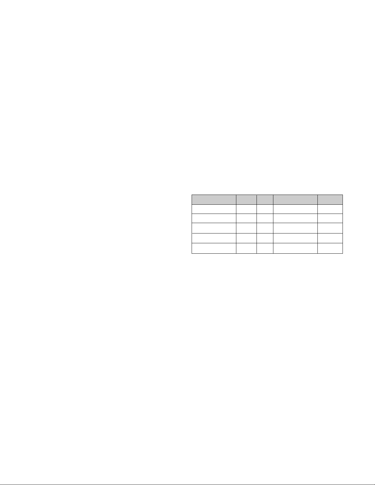
TIMING CHART
- 4 -
VIDEO
SYNC
B
D
C
F
E
A
H / V
H (Pixels)
V (Lines)
H (Pixels)
V (Lines)
H (Pixels)
V (Lines)
H (Pixels)
V (Lines)
H (Pixels)
V (Lines)
H (Pixels)
V (Lines)
H (Pixels)
V (Lines)
H (Pixels)
V (Lines)
H (Pixels)
V (Lines)
H (Pixels)
V (Lines)
H (Pixels)
V (Lines)
H (Pixels)
V (Lines)
H (Pixels)
V (Lines)
H (Pixels)
V (Lines)
Sync
Polarity
+
–
–
+
–
–
–
–
–
–
–
–
+
+
+
+
+
+
+
+
–
–
–
–
–
–
+
+
Dot
Clock
25.175
28.322
25.175
30.24
31.5
31.5
36.0
40.0
50.0
49.5
57.2832
65
75
78.75
Frequency
31.468 KHz
70.0 Hz
31.468 KHz
70.0 Hz
31.469 KHz
60.0 Hz
35.00 KHz
66.67 Hz
37.861 KHz
72.8 Hz
37.50 KHz
75.0 Hz
35.156KHz
56.25 Hz
37.879 KHz
60.3 Hz
48.077 KHz
72.188 Hz
46.875 KHz
75.0 Hz
49.725 KHz
74.55 Hz
48.363 KHz
60.0 Hz
56.476 KHz
70.0 Hz
60.023 KHz
75.0 Hz
Resolution
640 x 350
720 x 400
640 x 480
640 x 480
640 x 480
640 x 480
800 x 600
800 x 600
800 x 600
800 x 600
832 x 624
1024 x 768
1024 x 768
1024 x 768
Total
Period
( E )
800
449
900
449
800
525
864
525
832
520
840
500
1024
625
1056
628
1040
666
1056
625
1152
667
1344
806
1328
806
1312
800
Video
Active
Time ( A )
640
350
720
400
640
480
640
480
640
480
640
480
800
600
800
600
800
600
800
600
832
624
1024
768
1024
768
1024
768
Blanking
Time
( B )
160
99
180
49
160
45
224
45
192
40
200
20
224
25
256
28
240
66
256
25
320
43
320
38
304
38
288
32
Sync
Duration
( D )
96
2
108
2
96
2
64
3
40
3
64
3
72
2
128
4
120
6
80
3
64
3
136
6
136
6
96
3
Back
Porch
( F )
48
60
55
34
48
33
96
39
128
28
120
16
128
22
88
23
64
23
160
21
224
39
160
29
144
29
176
28
Front
Porch
( C )
16
37
17
13
16
10
64
3
24
9
16
1
24
1
40
1
56
37
16
1
32
1
24
3
24
3
16
1
MODE
1
2
3
4
5
6
7
8
9
10
11
12
13
14
(MAC)
(TEXT)
Page 5
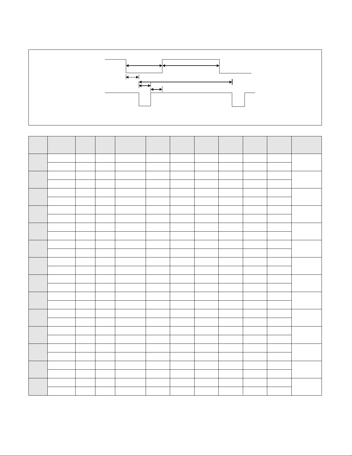
EEPROM
24LC16
ADC/PLL/Scaler
(GMZAN2)
MICOM
(MTV312)
Schmitt Trigger
(74HCT14A)
Panel
Interface
20 Pin
Connector
RGB
H.V
DSub
15P
E-DDC
Control
SCLK
SDATA
CON
8P
3.3VD
3.3V_PL
Module Power 3.3V
3.3V_PL3.3VD
5VR
3.3V_AD
Regulator
BA033
Regulator
BA033
3.3V_A
+3.3V
Regulator
BA033
Hsync2 Vsync2
Hsyncm
Vsyncm
2.5V_A 2.5V_D
Regulator
RC117
+2.5V_A
2.5V_D
5VR
LVDS
Filter
BD
SMPS
5VR
CON 8P
Inverter block
12VS
LIPS
CON 2P
EEPROM
24LC02
24 Bit
Inverter on/off
DIMADJ
Inverter on/off
DIMADJ
Inverter on/off
DIMADJ
Inverter on/off
DIMADJ
CON 2P
PWM
Controller
Page 6

DESCRIPTION OF BLOCK DIAGRAM
- 8 -
1. Scaler One chip IC(GMZAN-2, U201)
GMZAN-2 (U201) is one chip IC which it supports four internal function blocks of Video Amp, PLL,
A/D converter and Video processor.
Video signal (0.7Vp.p) clamped through C207, 208, 209 with matching IC’s proper cut off voltage.
This signal is processed as a proper 8 bit digital signal by U201’s amplifying, phase locking, A/D converting,
and scaling operations.
U201 outputs 24bit RGB data and control signals(Clock, Horizontal and Vertical sync, and Data Enable)
as LVDS IC’s input signals.
2. System Controller (Microprocessor) Circuit
1) Microprocessor (U501) distinguishes polarity and frequency by calculating horizontal and vertical sync input
from signal source.
2) Microprocessor (U501) carries out power control by sending power-down trigger signal to each IC.
3) Microprocessor (U501) communicates with EEPROM (U502), and GMZAN-2 (U201)
through IIC(2 lines) or 4 bit bus line. It makes all devices operated properly.
4) Microprocessor (U501) let User adjust screen by OSD function.
3. LVDS(Low Voltage Differential Signal, U411)
LVDS transmitter (U411) delivers digital signal to the receiver inside LCD module by method of abstraction.
The abstracted signals are pairs of RIN0+-, RIN1+-, RIN2+-, RIN3+-, and RCLKIN+- of which voltage swing
is 0.5V each.
When SHUTON pin’s input is High, transmitter goes to power down mode.
4. DC/DC block
This block is composed of regulators which supplies 2.5V and 3.3V.
Each regulator’s source power is 5VR from LIPS(LCD Inverter and Power Supply) block.
U806 supplies 2.5VD and 2.5VA and U802 supplies 3.3VD, 3.3V_AD, and 3.3V_PL powers to GMZAN-2’s
internal PLL, ADC, Pre-amp, and scaler by dropping down 5VR.
U805 supplies MODPWR-3.3V for LCD module’s operation by dropping down 5VR.
5. LIPS Block (LCD Inverter and Power Supply)
This block supplies DC voltages of 5VS to interface board and 12V to inverter by converting AC input voltage
of 100~240Vac.
Converting method is SMPS(Switching Mode Power Supply).
Inverter on/off signal from microprocessor makes inverter turned on or off .
DIMADJ signal from microprocessor does inverter’s current adjustment for Brightness control.
Page 7
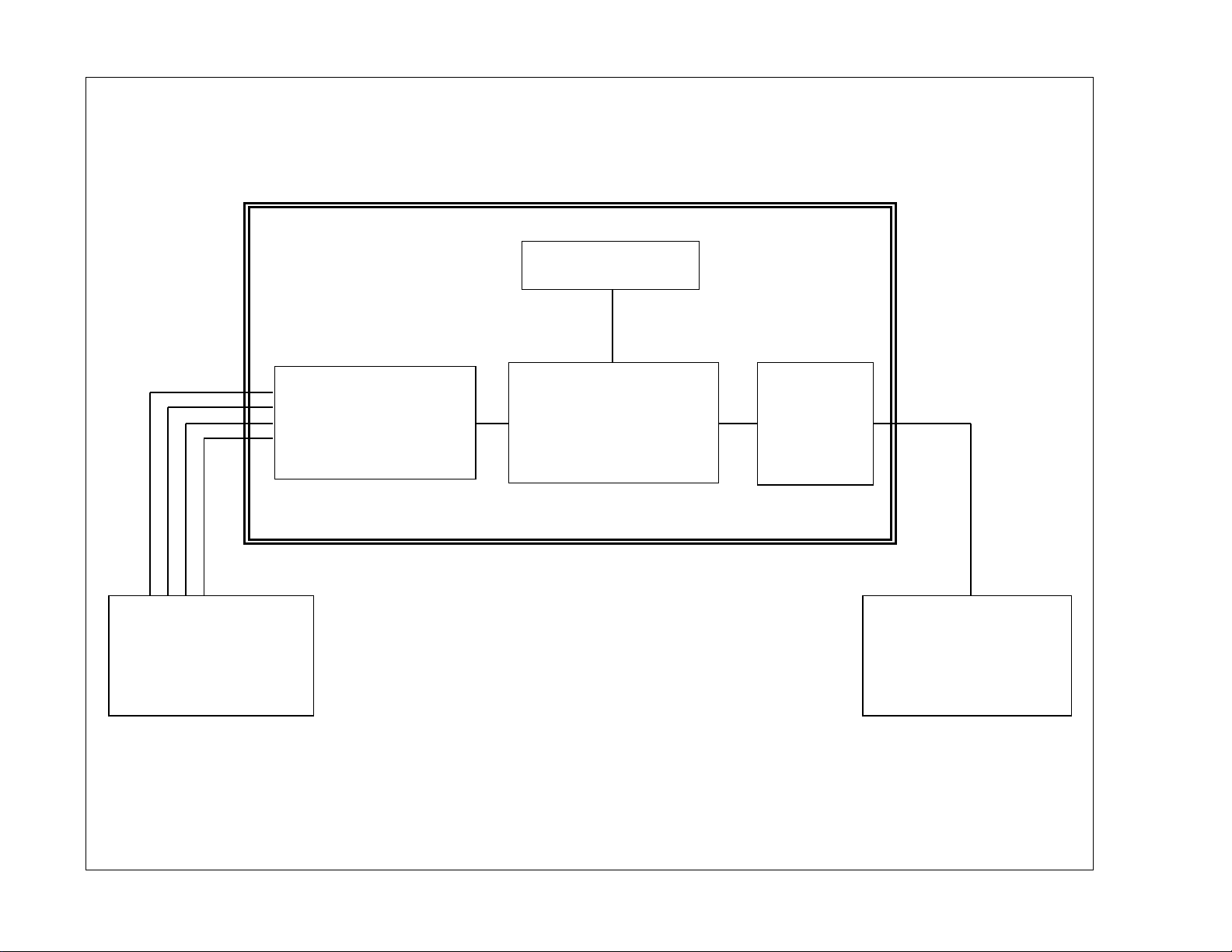
USB Touchscreen Constroller Block Diagram
- 9 -
4-Wire
Touch Panel
EEPROM
Burr-Brown
ADS7846
Masked OTP
or
Processor
Main System
Processor
PDIUS
BD12
Chip
Page 8

- 10 -
ADJUSTMENT
All adjustment are thoroughly checked and corrected
when the monitor leaves the factory, but sometimes
several minor adjustment may be required.
Adjustment should be following procedure and after
warming up for a minimum of 10 minutes.
Alignment appliances and tools.
- IBM Compatible PC
- Programmable Signal Generator.
(eg. VG-819 made by Astrodesign Co.)
- E(E)PROM with each mode data saved.
- Alignment Adapter and Software.
1. Adjustment for Factory Preset Mode
1) Run alignment program for L1510SFK on the IBM
compatible PC.
2) Select EEPROM All Init. command and Enter.
3) Display cross hatch pattern at Mode 1.
4) Select EDID WRITE command and Enter.
2. Adjustment for White Balance
1) Display color 0,0 pattern at Mode 13.
2) Set External Bright to MAX position and Contrast to
MAX Position.
3) Select PRESET START → BIAS CAL command
and Enter.
4) No attempt to manually adjust, BIAS data is automatically adjusted and saved to the EEPROM.
5) Display color 15,0 pattern at Mode 13.
6) Select DRIVE CAL command and Enter.
7) Color 1 (9300K) and Color 2 (6500K) are
automatically adjusted and saved to the EEPROM.
8) Select PRESET EXIT command and Enter.
Figure 1. Cable Connection
220
IBM
Compatible PC
PARALLEL PORT
Power inlet (required)
Power LED
ST Switch
Power Select Switch
(110V/220V)
Control Line
Not used
RS232C
PARALLEL
V-SYNC
POWER
ST
VGS
MONITOR
E
E
V-Sync On/Off Switch
(Switch must be ON.)
F
F
A
A
B
B
C
C
15
10
5
5
69
1
1
1
14
13
25
6
5V
5V
5V
4.7K
4.7K
4.7K
74LS06
74LS06
OFF ON
OFF
ON
11
Video Signal
Generator
Page 9

- 11 -
TROUBLESHOOTING GUIDE
1. NO POWER
CHECK U803.
CHECK
U802 PIN 1
VOLTAGE
(5V) ?
NO
NO POWER
(POWER INDICATOR OFF)
CHECK POWER
BOARD, AND FIND
OUT A SHORT POINT
AS OPENING
EACH POWER LINE
CHECK J705
VOLTAGE
PIN5, PIN6 (5V)?
NO
CHECK 5VS LINE
(OPEN CHECK)
CHECK
U805 PIN 1 Voltage
(5V) ?
NO
CHECK IIC LINE
CONNECTION
(U501, U502)
CHECK U201 VCC,
XTAL, RESET
IS U201
PIN12 (3.3V)
VOLTAGE REPEATED
AS PULSE
SHAPE ?
NO
YES
YES
YES
NO PROBLEM
NO
CHECK KEY CONTROL
CONNECTOR ROUTINE
Page 10

- 12 -
2. NO RASTER (OSD IS NOT DISPLAYED) – LIPS
CHECK MICOM INV
ON/OFF PORT.
J705 PIN2
5V?
NO
NO RASTER
(OSD IS NOT DISPLAYED)
CHECK LIPS
J705
PIN5, PIN 6
5V?
NO
1. CONFIRM BRIGHTNESS
OSD CONTRL STATE.
2. CHECK MICOM DIM-ADJ
PORT
J705 PIN1
5V?
NO
LIPS
CHECK
PULSE AS
CONTACTING SCOPE
PROBE TO CAUTION LABEL.
(CONTACT PROBE TO
CAUTION LABEL.
CAN YOU SEE PULSE
AT YOUR
SCOPE?
NO
REPLACE CCFL LAMP
IN THE LCD MODULE
YES
YES
YES
YES
Page 11

- 13 -
1. CHECK PIN141, 142
SOLDERING CONDITION
2. CHECK X201
3. TROUBLE IN U201
U201
POWER PINS
3.3V?
NO
CHECK U802, U806
U201 PIN141, 142
OSCILLATE AS 20MHZ?
CHECK CONNECTION LINE
FROM U201 TO U401
NO
TROUBLE IN CABLE
OR LCD MODULE
CHECK U805
U401 PIN1
3.3V?
NO
YES
YES
YES
YES
3. NO RASTER (OSD IS NOT DISPLAYED) – gmZAN2
NO RASTER
(OSD IS NOT DISPLAYED)
U401/U411
PIN31 IS 65MHz CLOCK?
PIN27 IS 48KHz H-SYNC?
PIN28 IS 60Hz V-SYNC?
PIN30 IS 48KHz DEN?
IS PULSE APPEARED
AT SIGNAL PINS?
NO
Page 12

- 14 -
CHECK U802, U806
U201
POWER PIN
3.3V?
NO
1. CHECK PC
2. CHECK SIGNAL CABLE
& D-SUB CONNECTOR
LINE
CHECK
R,G,B INPUT?
U201 PIN 87, 91, 95
NO
CHECK H-SYNC LINE
(D-SUB→U701→MICOM
→U201 PIN150)
CHECK
H-SYNC INPUT
U201 PIN 150?
NO
YES
YES
YES
NO RASTER
(OSD IS DISPLAYED)
4. NO RASTER (OSD IS DISPLAYED) – gmZAN2
Page 13

- 18 -
DATE: 2002. 12. 16.
*S *AL LOC. NO. PART NO. DESCRIPTION / SPECIFICATION
C201 0CC100CK41A 10PF 1608 50V 5% R/TP NP0
C202 0CC100CK41A 10PF 1608 50V 5% R/TP NP0
C203 0CC100CK41A 10PF 1608 50V 5% R/TP NP0
C204 0CK104CK56A 0.1UF 1608 50V 10% R/TP X7R
C205 0CK103CK51A 0.01UF 1608 50V 10% R/TP B(Y
C206 0CK104CK56A 0.1UF 1608 50V 10% R/TP X7R
C207 0CK103CK51A 0.01UF 1608 50V 10% R/TP B(Y
C208 0CK103CK51A 0.01UF 1608 50V 10% R/TP B(Y
C209 0CK103CK51A 0.01UF 1608 50V 10% R/TP B(Y
C210 0CK103CK51A 0.01UF 1608 50V 10% R/TP B(Y
C211 0CK103CK51A 0.01UF 1608 50V 10% R/TP B(Y
C212 0CK103CK51A 0.01UF 1608 50V 10% R/TP B(Y
C214 0CK104CK56A 0.1UF 1608 50V 10% R/TP X7R
C215 0CK103CK51A 0.01UF 1608 50V 10% R/TP B(Y
C216 0CK104CK56A 0.1UF 1608 50V 10% R/TP X7R
C217 0CC220CK41A 22PF 1608 50V 5% R/TP NP0
C218 0CC220CK41A 22PF 1608 50V 5% R/TP NP0
C219 0CC220CK41A 22PF 1608 50V 5% R/TP NP0
C221 0CC220CK41A 22PF 1608 50V 5% R/TP NP0
C222 0CC220CK41A 22PF 1608 50V 5% R/TP NP0
C223 0CC180CK41A 18PF 1608 50V 5% R/TP NP0
C224 0CC180CK41A 18PF 1608 50V 5% R/TP NP0
C226 0CC680CK41A 68PF 1608 50V 5% R/TP NP0
C227 0CC220CK41A 22PF 1608 50V 5% R/TP NP0
C228 0CC220CK41A 22PF 1608 50V 5% R/TP NP0
C229 0CC220CK41A 22PF 1608 50V 5% R/TP NP0
C230 0CC080CK11A 8PF 1608 50V 0.5 PF R/TP NP0
C231 0CC220CK41A 22PF 1608 50V 5% R/TP NP0
C233 0CC220CK41A 22PF 1608 50V 5% R/TP NP0
C234 0CC220CK41A 22PF 1608 50V 5% R/TP NP0
C237 0CC220CK41A 22PF 1608 50V 5% R/TP NP0
C238 0CC220CK41A 22PF 1608 50V 5% R/TP NP0
C239 0CC220CK41A 22PF 1608 50V 5% R/TP NP0
C240 0CC220CK41A 22PF 1608 50V 5% R/TP NP0
C241 0CC220CK41A 22PF 1608 50V 5% R/TP NP0
C242 0CC220CK41A 22PF 1608 50V 5% R/TP NP0
C243 0CC220CK41A 22PF 1608 50V 5% R/TP NP0
C244 0CC220CK41A 22PF 1608 50V 5% R/TP NP0
C245 0CC220CK41A 22PF 1608 50V 5% R/TP NP0
C246 0CC220CK41A 22PF 1608 50V 5% R/TP NP0
C247 0CC220CK41A 22PF 1608 50V 5% R/TP NP0
C248 0CC220CK41A 22PF 1608 50V 5% R/TP NP0
C249 0CC220CK41A 22PF 1608 50V 5% R/TP NP0
C254 0CK103CK51A 0.01UF 1608 50V 10% R/TP B(Y
C255 0CK103CK51A 0.01UF 1608 50V 10% R/TP B(Y
C256 0CK103CK51A 0.01UF 1608 50V 10% R/TP B(Y
C257 0CK103CK51A 0.01UF 1608 50V 10% R/TP B(Y
C258 0CK103CK51A 0.01UF 1608 50V 10% R/TP B(Y
C259 0CK103CK51A 0.01UF 1608 50V 10% R/TP B(Y
C261 0CC680CK41A 68PF 1608 50V 5% R/TP NP0
C262 0CC680CK41A 68PF 1608 50V 5% R/TP NP0
C269 0CK103CK51A 0.01UF 1608 50V 10% R/TP B(Y
DATE: 2002. 12. 16.
*S *AL LOC. NO. PART NO. DESCRIPTION / SPECIFICATION
C270 0CK103CK51A 0.01UF 1608 50V 10% R/TP B(Y
C271 0CK103CK51A 0.01UF 1608 50V 10% R/TP B(Y
C401 0CK104CK56A 0.1UF 1608 50V 10% R/TP X7R
C402 0CK104CK56A 0.1UF 1608 50V 10% R/TP X7R
C403 0CK104CK56A 0.1UF 1608 50V 10% R/TP X7R
C404 0CK104CK56A 0.1UF 1608 50V 10% R/TP X7R
C405 0CK104CK56A 0.1UF 1608 50V 10% R/TP X7R
C501 0CK104CK56A 0.1UF 1608 50V 10% R/TP X7R
C502 0CC101CK41A 100PF 1608 50V 5% R/TP NP0
C503 0CC101CK41A 100PF 1608 50V 5% R/TP NP0
C504 0CK104CK56A 0.1UF 1608 50V 10% R/TP X7R
C505 0CC101CK41A 100PF 1608 50V 5% R/TP NP0
C506 0CC101CK41A 100PF 1608 50V 5% R/TP NP0
C507 0CK104CK56A 0.1UF 1608 50V 10% R/TP X7R
C508 0CK104CK56A 0.1UF 1608 50V 10% R/TP X7R
C509 0CK104CK56A 0.1UF 1608 50V 10% R/TP X7R
C512 0CC180CK41A 18PF 1608 50V 5% R/TP NP0
C513 0CC180CK41A 18PF 1608 50V 5% R/TP NP0
C514 0CH8106F611 10UF 16V M 85STD(CYL) R/TP
C515 0CC680CK41A 68PF 1608 50V 5% R/TP NP0
C516 0CK104CK56A 0.1UF 1608 50V 10% R/TP X7R
C703 0CK104CK56A 0.1UF 1608 50V 10% R/TP X7R
C706 0CK104CK56A 0.1UF 1608 50V 10% R/TP X7R
C707 0CC680CK41A 68PF 1608 50V 5% R/TP NP0
C712 0CC101CK41A 100PF 1608 50V 5% R/TP NP0
C713 0CK104CK56A 0.1UF 1608 50V 10% R/TP X7R
C715 0CH3105F946 1UF 16V Z F 2012 R/TP
C731 0CC680CK41A 68PF 1608 50V 5% R/TP NP0
C801 0CK103CK51A 0.01UF 1608 50V 10% R/TP B(Y
C802 0CK104CK56A 0.1UF 1608 50V 10% R/TP X7R
C813 0CK103CK51A 0.01UF 1608 50V 10% R/TP B(Y
C816 0CK104CK56A 0.1UF 1608 50V 10% R/TP X7R
C817 0CE107CF610 100UF SHL,SD 16V 20% BULK FL
C818 0CK104CK56A 0.1UF 1608 50V 10% R/TP X7R
C819 0CK103CK51A 0.01UF 1608 50V 10% R/TP B(Y
C820 0CE107CF610 100UF SHL,SD 16V 20% BULK FL
C821 0CK104CK56A 0.1UF 1608 50V 10% R/TP X7R
C824 0CH8107F611 100UF 16V M 85STD(CYL) R/TP
C825 0CE107CF610 100UF SHL,SD 16V 20% BULK FL
C826 0CK104CK56A 0.1UF 1608 50V 10% R/TP X7R
C827 0CK103CK51A 0.01UF 1608 50V 10% R/TP B(Y
C828 0CK104CK56A 0.1UF 1608 50V 10% R/TP X7R
C829 0CK103CK51A 0.01UF 1608 50V 10% R/TP B(Y
C831 0CH8107F611 100UF 16V M 85STD(CYL) R/TP
C832 0CH8107F611 100UF 16V M 85STD(CYL) R/TP
C835 0CK104CK56A 0.1UF 1608 50V 10% R/TP X7R
D701 0DSDI00038A BAV99 DIODES R/TP SOT23 100V
D702 0DSDI00038A BAV99 DIODES R/TP SOT23 100V
D703 0DSDI00038A BAV99 DIODES R/TP SOT23 100V
D704 0DSDI00038A BAV99 DIODES R/TP SOT23 100V
D705 0DSDI00038A BAV99 DIODES R/TP SOT23 100V
REPLACEMENT PARTS LIST
CAUTION: BEFORE REPLACING ANY OF THESE COMPONENTS,
READ CAREFULLY THE SAFETY PRECAUTIONS IN THIS MANUAL.
* NOTE : S SAFETY Mark
AL ALTERNATIVE PARTS
MAIN BOARD
CAPACITORS
DIODEs
Page 14

DATE: 2002. 12. 16.
*S *AL LOC. NO. PART NO. DESCRIPTION / SPECIFICATION
D706 0DSDI00038A BAV99 DIODES R/TP SOT23 100V
D707 0DSDI00018A BAT54 DIODES R/TP SOT23 30V
D708 0DSDI00018A BAT54 DIODES R/TP SOT23 30V
ZD701 0DZ560009GB BZT52C5V6S DIODES R/TP SOD32
ZD702 0DZ560009GB BZT52C5V6S DIODES R/TP SOD32
U201 0IPRPGA002A GMZAN2-160P GENESIS MICROCHI
U401 0ITH638300B THC63LVDM83R THINE 56P,TSSOP
U501 0IZZTSZ199A MYSON 42PIN BK OTP LB500K
U502 0ISG240860B M24C08W6 SGS-THOMSON 8SOP R/
U701 0IMO741420B MC74HCT14ADR2 14P,SOIC TP LE
U702 0ICS240213A CAT24WC02J-TE13 8P SOP TP 2K
U802 0IPMGKE011A KIA78D33F KEC DPAK R/TP 3.3V
U805 0IRH033000A BA033SFP P/MOLD-5 TP REGULAT
U806 0IPMGON007A NCP1117ST25T3 ON SEMI SOT223
L201 6210TCE001P HB-1S2012-121JT CERATECH 201
L202 6210TCE001P HB-1S2012-121JT CERATECH 201
L203 6210TCE001P HB-1S2012-121JT CERATECH 201
L204 6210TCE001P HB-1S2012-121JT CERATECH 201
L205 6210TCE001P HB-1S2012-121JT CERATECH 201
L401 6210TCE001G HH-1M3216-501 CERATEC 3216MM
L701 6210TCE001S HU-1M2012-121 CERATECH 2012M
L702 6210TCE001P HB-1S2012-121JT CERATECH 201
L703 6210TCE001P HB-1S2012-121JT CERATECH 201
L704 6210TCE001P HB-1S2012-121JT CERATECH 201
L705 6210TCE001P HB-1S2012-121JT CERATECH 201
L706 6210TCE001P HB-1S2012-121JT CERATECH 201
L707 6210TCE001P HB-1S2012-121JT CERATECH 201
L710 6210TCE001G HH-1M3216-501 CERATEC 3216MM
L801 6210TCE001G HH-1M3216-501 CERATEC 3216MM
L802 6210TCE001G HH-1M3216-501 CERATEC 3216MM
L803 6210TCE001G HH-1M3216-501 CERATEC 3216MM
L804 6210TCE001G HH-1M3216-501 CERATEC 3216MM
L805 6210TCE001G HH-1M3216-501 CERATEC 3216MM
Q502 0TRDI80002A MMBT3904 DIODES R/TP SOT23 6
Q503 0IKE704200H KIA7042AP TO-92 TP 4.2 VOLT
Q701 0TRDI80002A MMBT3904 DIODES R/TP SOT23 6
R201 0RJ4701D677 4.7K OHM 1/10 W 5% 1608 R/TP
R202 0RJ4701D677 4.7K OHM 1/10 W 5% 1608 R/TP
R203 0RJ1000D677 100 OHM 1/10 W 5% 1608 R/TP
R204 0RJ1000D677 100 OHM 1/10 W 5% 1608 R/TP
R205 0RJ1000D677 100 OHM 1/10 W 5% 1608 R/TP
R206 0RJ2701D677 2.7K OHM 1/10 W 5% 1608 R/TP
R207 0RJ0472D677 47 OHM 1/10 W 5% 1608 R/TP
R208 0RJ1000D677 100 OHM 1/10 W 5% 1608 R/TP
R209 0RJ1000D677 100 OHM 1/10 W 5% 1608 R/TP
R210 0RJ1000D677 100 OHM 1/10 W 5% 1608 R/TP
R401 0RJ1002D677 10K OHM 1/10 W 5% 1608 R/TP
R403 0RJ1001D677 1K OHM 1/10 W 5% 1608 R/TP
R404 0RJ5601D477 5.6K OHM 1/10 W 1% 1608 R/TP
R501 0RJ4701D677 4.7K OHM 1/10 W 5% 1608 R/TP
DATE: 2002. 12. 16.
*S *AL LOC. NO. PART NO. DESCRIPTION / SPECIFICATION
R502 0RJ4701D677 4.7K OHM 1/10 W 5% 1608 R/TP
R503 0RJ4701D677 4.7K OHM 1/10 W 5% 1608 R/TP
R504 0RJ4701D677 4.7K OHM 1/10 W 5% 1608 R/TP
R505 0RJ1002D677 10K OHM 1/10 W 5% 1608 R/TP
R506 0RJ4701D677 4.7K OHM 1/10 W 5% 1608 R/TP
R507 0RJ1002D677 10K OHM 1/10 W 5% 1608 R/TP
R508 0RJ1002D677 10K OHM 1/10 W 5% 1608 R/TP
R509 0RJ4701D677 4.7K OHM 1/10 W 5% 1608 R/TP
R510 0RJ1000D677 100 OHM 1/10 W 5% 1608 R/TP
R511 0RJ4701D677 4.7K OHM 1/10 W 5% 1608 R/TP
R512 0RJ4701D677 4.7K OHM 1/10 W 5% 1608 R/TP
R513 0RJ1002D677 10K OHM 1/10 W 5% 1608 R/TP
R515 0RJ1000D677 100 OHM 1/10 W 5% 1608 R/TP
R516 0RJ4701D677 4.7K OHM 1/10 W 5% 1608 R/TP
R517 0RJ4701D677 4.7K OHM 1/10 W 5% 1608 R/TP
R518 0RJ4701D677 4.7K OHM 1/10 W 5% 1608 R/TP
R519 0RJ4701D677 4.7K OHM 1/10 W 5% 1608 R/TP
R520 0RJ4701D677 4.7K OHM 1/10 W 5% 1608 R/TP
R521 0RJ4701D677 4.7K OHM 1/10 W 5% 1608 R/TP
R522 0RJ1500D677 150 OHM 1/10 W 5% 1608 R/TP
R523 0RJ0332D677 33 OHM 1/10 W 5% 1608 R/TP
R524 0RJ0332D677 33 OHM 1/10 W 5% 1608 R/TP
R525 0RJ1000D677 100 OHM 1/10 W 5% 1608 R/TP
R526 0RJ4701D677 4.7K OHM 1/10 W 5% 1608 R/TP
R527 0RJ4701D677 4.7K OHM 1/10 W 5% 1608 R/TP
R528 0RJ1000D677 100 OHM 1/10 W 5% 1608 R/TP
R529 0RJ1000D677 100 OHM 1/10 W 5% 1608 R/TP
R530 0RJ1000D677 100 OHM 1/10 W 5% 1608 R/TP
R531 0RJ1000D677 100 OHM 1/10 W 5% 1608 R/TP
R532 0RJ3301D677 3.3K OHM 1/10 W 5% 1608 R/TP
R533 0RJ0332D677 33 OHM 1/10 W 5% 1608 R/TP
R534 0RJ0332D677 33 OHM 1/10 W 5% 1608 R/TP
R535 0RJ3301D677 3.3K OHM 1/10 W 5% 1608 R/TP
R536 0RJ1004D677 1000000 OHM 1/10 W 5% 1608 R
R537 0RJ4701D677 4.7K OHM 1/10 W 5% 1608 R/TP
R540 0RJ1002D677 10K OHM 1/10 W 5% 1608 R/TP
R541 0RJ1000D677 100 OHM 1/10 W 5% 1608 R/TP
R551 0RJ0000D677 0 OHM 1/10 W 5% 1608 R/TP
R561 0RJ0000D677 0 OHM 1/10 W 5% 1608 R/TP
R571 0RJ0000D677 0 OHM 1/10 W 5% 1608 R/TP
R581 0RJ0000D677 0 OHM 1/10 W 5% 1608 R/TP
R701 0RJ0752D677 75 OHM 1/10 W 5% 1608 R/TP
R703 0RJ0752D677 75 OHM 1/10 W 5% 1608 R/TP
R705 0RJ4700D677 470 OHM 1/10 W 5% 1608 R/TP
R706 0RJ0752D677 75 OHM 1/10 W 5% 1608 R/TP
R707 0RJ0272D677 27 OHM 1/10 W 5% 1608 R/TP
R708 0RJ1500D677 150 OHM 1/10 W 5% 1608 R/TP
R709 0RJ1500D677 150 OHM 1/10 W 5% 1608 R/TP
R711 0RJ0000D677 0 OHM 1/10 W 5% 1608 R/TP
R712 0RJ1000D677 100 OHM 1/10 W 5% 1608 R/TP
R713 0RJ1000D677 100 OHM 1/10 W 5% 1608 R/TP
R714 0RJ1000D677 100 OHM 1/10 W 5% 1608 R/TP
R715 0RJ4701D677 4.7K OHM 1/10 W 5% 1608 R/TP
R716 0RJ4701D677 4.7K OHM 1/10 W 5% 1608 R/TP
R717 0RJ4701D677 4.7K OHM 1/10 W 5% 1608 R/TP
R722 0RJ1001D677 1K OHM 1/10 W 5% 1608 R/TP
R723 0RJ0332D677 33 OHM 1/10 W 5% 1608 R/TP
R724 0RJ0332D677 33 OHM 1/10 W 5% 1608 R/TP
R725 0RJ4701D677 4.7K OHM 1/10 W 5% 1608 R/TP
R726 0RJ4701D677 4.7K OHM 1/10 W 5% 1608 R/TP
R727 0RJ4701D677 4.7K OHM 1/10 W 5% 1608 R/TP
R733 0RJ1501D677 1.5K OHM 1/10 W 5% 1608 R/TP
- 19 -
COILs & COREs
TRANSISTOR
ICs
RESISTORs
Page 15

DATE: 2002. 12. 16.
*S *AL LOC. NO. PART NO. DESCRIPTION / SPECIFICATION
R734 0RJ4701D677 4.7K OHM 1/10 W 5% 1608 R/TP
R805 0RJ1001D677 1K OHM 1/10 W 5% 1608 R/TP
R807 0RJ1003D677 100K OHM 1/10 W 5% 1608 R/TP
R813 0RJ1001D677 1K OHM 1/10 W 5% 1608 R/TP
RA501 0RHZTCZ001A 100 OHM 1/16 W 5% 3215 R/TP
RA502 0RHZTCZ001A 100 OHM 1/16 W 5% 3215 R/TP
X201 6212AA2004B HC-49U TXC 20.0MHZ +/- 30 PP
X501 6212AA2004A HC-49U TXC 12.0MHZ +/- 30 PP
LED1 0DLLT0148AA LITEON LTST-C195KGJSKT R/TP
R1 0RJ4701D677 4.7K OHM 1/10 W 5% 1608 R/TP
R2 0RJ4701D677 4.7K OHM 1/10 W 5% 1608 R/TP
R3 0RJ1501D677 1.5K OHM 1/10 W 5% 1608 R/TP
R4 0RJ1501D677 1.5K OHM 1/10 W 5% 1608 R/TP
R5 0RJ3301D677 3.3K OHM 1/10 W 5% 1608 R/TP
R6 0RJ3301D677 3.3K OHM 1/10 W 5% 1608 R/TP
R7 0RJ9101D677 9.1K OHM 1/10 W 5% 1608 R/TP
SW1 140-058E SKHV10910B LGEC NON 12V 20A
SW2 140-058E SKHV10910B LGEC NON 12V 20A
SW3 140-058E SKHV10910B LGEC NON 12V 20A
SW4 140-058E SKHV10910B LGEC NON 12V 20A
SW5 140-058E SKHV10910B LGEC NON 12V 20A
SW6 140-058E SKHV10910B LGEC NON 12V 20A
SW7 140-058E SKHV10910B LGEC NON 12V 20A
ZD1 0DZ560009GB BZT52C5V6S DIODES R/TP SOD32
ZD2 0DZ560009GB BZT52C5V6S DIODES R/TP SOD32
- 20 -
OTHERs
CONTROL BOARD
Page 16

CAT24WC02J-TE13 8P
A
0
A
1
A
2
V
SS
V
CC
WP
SCL
SDA
A
0
A
1
A
2
V
SS
V
CC
WP
SCL
SDA
1
2
3
4
8
7
6
5
1
2
3
4
8
7
6
5
A
0
A
1
A
2
V
SS
V
CC
WP
SCL
SDA
1
2
3
4
8
7
6
5
V
A1
Y1
AS
A2
Y6
Y2
A5
A3
Y5
Y3
A4
GND
Y4
CC
1
2
3
4
5
6
7
14
13
12
11
10
9
8
DIP Package(p) SOIX Package(J)
BLOCK DIAGRAM
EXTERNAL LOAD
PIN CONFIGURATION
PIN FUNCTION
Pin Name
A0, A1, A2
SDA
SCL
WP
Vcc
TSSOP Package(U)
Function
Device Adress Inputs
Serial Data/Address
Serial Clock
Write Protect
+1.8V to + 6.0V power Supply
V
V
SDA
WP
SCL
CC
SS
D
OUT
ACK
WORD ADDRESS
BUFFERS
START/STOP
LOGIC
XDEC
CONTROL
LOGIC
STATE COUNTERS
A
0
A
1
A
2
SLAVE
ADDRESS
COMPARATORS
SENSE AMPS
SHIFT REGISTERS
COLUMN
DECODERS
2
E PROM
DATA IN STORAGE
HIGH VOLTAGE/
TIMING CONTROL
Vss
Ground
MC74HCT14ADR2 14P
BLOCK DIAGRAM
PIN CONFIGURATION
12
A1 Y1
34
A2 Y2
56
A3 Y3
98
A4 Y4
11 10
A5 Y5
13 12
A6
PIN 14=V
PIN 7=GND
Y6
CC
Page 17

THC63LVDM83R
1
2
3
4
5
6
7
8
9
10
11
12
13
14
15
16
17
18
19
20
21
22
23
24
25
26
27
28
56
55
54
53
52
51
50
49
48
47
46
45
44
39
38
37
36
35
34
33
32
31
30
29
43
42
41
40
RS
TD1
TA5
TA6
GND
TB0
TB1
TD2
VCC
TD3
TB2
TB3
GND
TB4
TB5
TD4
R/F
TD5
TB6
TC0
GND
TC1
TC2
TC3
TD6
VCC
TC4
TC5
TA4
TA3
TA2
GND
TA1
TA0
TD0
LVDS GND
TATA+
TBTB+
LVDS VCC
LVDS GND
TCTC+
TCLK -
TCLK+
TDTD+
LVDS GND
PLL GND
PLL VCC
PLL GND
/PDWN
CLK IN
TC6
GND
THC63LVDM83R
DATA
(LVDS)
TA0-6
TB0-6
TC0-6
TD0-6
7
7
7
7
TRANSMITTER
CLOCK IN
(20 to 85MHz)
R/F
/PDWN
RS
TB +/-
TA +/-
TC +/-
TD +/-
(140-595Mbit/On Each
LVDS Channel)
TCLK +/CLOCK
(LVDS)
20~85MHz
TTL PARALLEL TO SERIAL
PLL
THC63LVDM83R
PIN CONFIGURATION BLOCK DIAGRAM
Page 18

1. GMZAN2
Page 19

2. LVDS
Page 20

3. MICOM
Page 21

4. DC/DC BLOCK
Page 22

5. CONNECTOR & JACKS
 Loading...