

LG L1150 Service Manual

Service Manual
Model : L1150
Service Manual
L1150
P/N : MMBD0034601 Date: June, 2004 / Issue 1.0

* The information in this manual is subject to change without notice and should not be construed as a
commitment by LGE Inc. Furthermore, LGE Inc. reserves the right, without notice, to make changes to
equipment design as advances in engineering and manufacturing methods warrant.
* This manual provides the information necessary to install, program, operate and maintain the L1150.
REVISED HISTORY
Editor Date Issue Contents of Changes S/W Version
Y.M. CHO 29/DEC/2003 Issue 0.1 INITIAL RELEASE
Y.M. CHO 25/JAN/2004 Issue 0.2 SECOND RELEASE


- 3 -
1. Introduction..................................... 5
1.1 Purpose................................................... 5
1.2 Regulatory Information............................ 5
1.2.1. Security........................................ 5
1.2.2. Incidence of Harm........................ 5
1.2.3. Changes in Service...................... 5
1.2.4. Maintenance Limitations .............. 5
1.2.5. Notice of Radiated Emissions...... 6
1.2.6. Pictures........................................ 6
1.2.7. Interference and Attenuation ....... 6
1.2.8. Electrostatic Sensitive Devices.... 6
1.3 Abbreviation ............................................ 6
2. General Performance...................... 8
2.1 H/W Feature............................................ 8
2.2 Technical Specification ......................... 10
3. H/W Circuit Description................ 15
3.1. RF Circuit ............................................. 15
3.1.1. Front End Part ........................... 15
3.1.2. Receiver Part ............................. 16
3.1.3. Synthesizer Part ........................ 18
3.1.4. Transmitter Part ......................... 19
3.1.5. Power Amplifier.......................... 20
3.1.6. 26 MHz Clock ............................ 20
3.1.7. Power Supplies and
Control Signals .......................... 21
3.2. Digital Baseband(DBB) Processor....... 22
3.2.1. General Description ................... 22
3.2.2. Block Description ....................... 23
3.2.3. External Devices connected to
memory interface ....................... 24
3.2.4. RF Interface
(TPU, TSP block)....................... 24
3.2.5. SIM interface.............................. 24
3.2.6. UART Interface .......................... 25
3.2.7. GPIO map.................................. 26
3.3. Analog Baseband(ABB) Processor...... 27
3.3.1. General Description ................... 27
3.3.2. Audio Signal Processing &
Interface..................................... 28
3.3.3. Audio uplink processing............. 28
3.3.4. Audio downlink processing ........ 29
3.3.5. Baseband Codec (BBC) ............ 30
3.3.6. Voltage Regulation (VREG)....... 31
3.3.7. ADC Channels ........................... 32
3.3.8. Charging .................................... 33
3.3.9. Switch ON/OFF.......................... 33
3.3.10. Memory.................................... 34
3.3.11. Display & FPC Interface .......... 34
3.3.12. Keypad Switching &
Scanning.................................. 36
3.3.13. Keypad back-light
Illumination............................... 37
3.3.14. LCD Illumination ...................... 37
3.4. Camera Circuit ..................................... 38
A. BaseBand Components
(Component Side) ........................... 41
B. BaseBand Components
(Keypad Side).................................. 42
C. Digital Baseband (DBB)
Processor ........................................ 42
D. Analog Main Processor (ABB) ........ 43
E. Memory ........................................... 44
F. Voltage Regulation (LDO) ............... 45
G. MIDI ................................................ 46
H. Charging.......................................... 46
I. KEY Back-light Illumination............... 47
J. SIM................................................... 47
K. Keypad ............................................ 48
L. Infrared ............................................ 48
M. CAMERA ........................................ 49
N. Charge Indicating LED .................... 49
Table of Contents

- 4 -
4. TROUBLE SHOOTING .................. 50
4.1. Baseband Components
(Component Side)................................ 50
4.2. Baseband Components
(Keypad Side) ...................................... 51
4.3. Power On Trouble................................ 52
4.4. Charging Trouble ................................. 53
4.5. LCD Display Trouble............................ 55
4.6. Speaker/Receiver Trouble ................... 57
A. Receiver Trouble ............................. 59
B. Speaker Trouble.............................. 60
4.7. Microphone Trouble ............................. 61
4.8. Vibrator Trouble ................................... 63
4.9. Keypad Backlight Trouble .................... 65
4.10. Folder ON/OFF Trouble ..................... 67
4.11. SIM Detect Trouble ............................ 69
4.12. CAMERA Trouble .............................. 71
4.13. Earphone Trouble .............................. 75
4.14. Infrared Data Association Trouble ..... 79
4.15. The Block Diagram of the RF Part ..... 81
4.16. Tx / Rx Part Description ..................... 83
4.17. Receiver Part Description .................. 85
4.18. Transmitter Part Description .............. 89
4.19. RX Part Trouble Shooting .................. 92
4.20. TX Part Trouble Shooting .................. 97
5. DISASSEMBLY INSTRUCTION... 101
6. DOWNLOAD AND
CALIBRATION ............................. 106
7. BLOCK DIAGRAM....................... 112
8. CIRCUIT DIAGRAM ..................... 113
9. PCB LAYOUT............................... 121
10. STAND ALONE TEST &
CALIBRATION ........................... 123
A. What is Standalone Test? ............. 123
B. Standalone Test
Equipment Setup........................... 123
C. Rx Standalone Test....................... 124
D. Tx Standalone Test ....................... 124
E. What is Calibration? ...................... 125
F. Calibration program ....................... 126
G. Calibration Equipment Setup ........ 127
H. Calibrate L1150 with ChiWoo........ 128
I. Setup and Test with LAPUTA ......... 129
11. EXPLODED VIEW &
REPLACEMENT PART LIST ..... 133
11.1 EXPLODED VIEW ............................ 133
11.2 Replacement Parts
<Mechanic component>.................... 135
<Main component> ........................... 138
11.3 Accessory ......................................... 150

1. Introduction
- 5 -
1.1. Purpose
This manual provides the information necessary to repair, calibration, description and download the
features of the L1150.
1.2. Regulatory Information
1.2.1. Security
Toll fraud, the unauthorized use of telecommunications system by an unauthorized part (for example,
persons other than your company’s employees, agents, subcontractors, or person working on your
company’s behalf) can result in substantial additional charges you’re your telecommunications
services. System users are responsible for the security of own system. There are may be risks of toll
fraud associated with your telecommunications system. System users are responsible for
programming and configuring the equipment to prevent unauthorized use. LGE does not warrant that
this product is immune from the above case but will prevent unauthorized use of common-carrier
telecommunication service of facilities accessed through or connected to it. LGE will not be
responsible for any charges that result from such unauthorized use.
1.2.2. Incidence of Harm
If a telephone company determines that the equipment provided to customer is faulty and possibly
causing harm or interruption in service to the telephone network, it should disconnect telephone
service until repair can be done. A telephone company may temporarily disconnect service as long as
repair is not done.
1.2.3. Changes in Service
A local telephone company may make changes in its communications facilities or procedure. If these
changes could reasonably be expected to affect the use of the L1150 or compatibility with the network,
the telephone company is required to give advanced written notice to the user, allowing the user to
take appropriate steps to maintain telephone service.
1.2.4. Maintenance Limitations
Maintenance limitations on the L1150 must be performed only by the LGE or its authorized agent. The
user may not make any changes and/or repairs expect as specifically noted in this manual. Therefore,
note that unauthorized alternations or repair may affect the regulatory status of the system and may
void any remaining warranty.
1. Introduction

1. Introduction
- 6 -
1.2.5. Notice of Radiated Emissions
The L1150 complies with rules regarding radiation and radio frequency emission as defined by local
regulatory agencies. In accordance with these agencies, you may be required to provide information
such as the following to the end user.
1.2.6. Pictures
The pictures in this manual are for illustrative purposes only; your actual hardware may look slightly
different.
1.2.7. Interference and Attenuation
An L1150 may interfere with sensitive laboratory equipment, medical equipment, etc. Interference from
unsuppressed engines or electric motors may cause problems.
1.2.8. Electrostatic Sensitive Devices
ATTENTION
Boards, which contain Electrostatic Sensitive Device (ESD), are indicated by the sign. Following
information is ESD handling: Service personnel should ground themselves by using a wrist strap when
exchange system boards.
When repairs are made to a system board, they should spread the floor with anti-static mat which is
also grounded. Use a suitable, grounded soldering iron. Keep sensitive parts in these protective
packages until these are used. When returning system boards or parts such as EEPROM to the
factory, use the protective package as described.
1.3 Abbreviation
Para os propósitos do manual, a seguir as abreviações aplicadas.
APC Automatic Power Control
BB Baseband
BER Bit Error Ratio
CC-CV Constant Current ? Constant Voltage
CLA Cigar Lighter Adapter
DAC Digital to Analog Converter
DCS Digital Communication System
dBm dB relative to 1 milliwatt
DSP Digital Signal Processing
EEPROM Electrical Erasable Programmable Read-Only Memory
1. Introduction
- 7 -
EL Electroluminescence
ESD Electrostatic Discharge
FPCB Flexible Printed Circuit Board
GMSK Gaussian Minimum Shift Keying
GPIB General Purpose Interface Bus
GPRS General Packet Radio Service
GSM Global System for Mobile Communications
IPUI International Portable User Identity
IF Intermediate Frequency
LCD Liquid Crystal Display
LDO Low Drop Output
LED Light Emitting Diode
LGE LG Electronics
OPLL Offset Phase Locked Loop
PAM Power Amplifier Module
PCB Printed Circuit Board
PGA Programmable Gain Amplifier
PLL Phase Locked Loop
PSTN Public Switched Telephone Network
RF Radio Frequency
RLR Receiving Loudness Rating
RMS Root Mean Square
RTC Real Time Clock
SAW Surface Acoustic Wave
SIM Subscriber Identity Module
SLR Sending Loudness Rating
SRAM Static Random Access Memory
STMR Side Tone Masking Rating
TA Travel Adapter
TDD Time Division Duplex
TDMA Time Division Multiple Access
UART Universal Asynchronous Receiver/Transmitter
VCO Voltage Controlled Oscillator
VCTCXO Voltage Control Temperature Compensated Crystal Oscillator
WAP Wireless Application Protocol
2. General Performance
- 8 -
2.1 H/W Feature
A. Hardware Feature
• GSM 850 / DCS 1800/ PCS 1900 Tri-Band
• 65k Color-TFT(128x160) Main LCD, 4 Gray Mono
(96x64) Sub LCD
• 950mAh Li-Ion Battery
• 3 V plug-in type SIM card socket
• 40 poly MIDI sound Ring-tone
• Jack type Ear-microphone
• Dimension : 89.0 X 46.5 X 23.6 mm, Weight : 95 g
• Built-in Camera : 330K CMOS Camera (VGA)
B. Software Feature
• WAP, Java Supported
• GPRS Class 10 Compatible
• FR/EFR/AMR Speech Coding
• 5-Level Volume Control (Voice, Ringtone, etc..)
• SMS/EMS
• Phone Book
– Total 255 Members
• Voice Memo
– Maximum 3 Memos
– Maximum 30 seconds per each memo
• Language : English…
• eZi Text
2. General Performance
2. General Performance
- 9 -
Item Feature Comment
Standard Battery Li-ion, 950mAh
..AVG TCVR Current 250mA
Standby Current < 5.2mA
Talk time At least 3.5 hours at PL5. (GSM 850)
At least 4.5 hours at PL0. (1800/1900)
Standby time up to 250 hours at DRX 6.
Charging time 3 hours
RX Sensitivity GSM850 : -105dBm, DCS/PCS : -105dBm
TX output power GSM850: 33dBm (Level 5)
DCS/PCS: 30dBm (Level 0)
GPRS compatibility Class 10
SIM card type 3V Small
Display 65K TFT(128x160) Main LCD, 4Gray Mono(96x64) Sub LCD
Soft icons
Key Pad
Status Indicator 0 ~ 9, #, *, Navigation Key, Up/Down Side Key
Camera side key, Confirm Key,
Send Key, END/PWR Key
ANT External
EAR Phone Jack 3 pole earphone jack
PC Synchronization Yes
Speech coding EFR/FR/AMR/HR
Data and Fax Yes
Vibrator Yes
Buzzer No
Voice Recoding Yes
C-Mic Yes
Receiver Yes
Travel Adapter Yes
Options CLA, Data Kit
2. General Performance
- 10 -
2.2 Technical Specification
Item Description Specification
GSM850
⍥TX: 824.2 + 0.2*(n-128) (n=128 ~ 251)
⍥RX: TX + 45 MHz
DCS1800
1 Frequency Band ⍥TX: 1710 + ( n-511 ) x 0.2 MHz (n = 512 ~ 885)
⍥RX: TX + 95 MHz
PCS1900
⍥TX: 1850 + ( n-511 ) x 0.2 MHz
⍥RX: 1930 + ( n-511 ) x 0.2 MHz (n = 512 ~ 810)
2 Phase Error
RMS < 5 degrees
Peak < 20 degrees
3 Frequency Error < 0.1ppm
GSM850
Level Power Toler. Level Power Toler.
5 33 dBm
ᴦ
2dB 13 17 dBm
ᴦ
3dB
6 31 dBm
ᴦ
3dB 14 15 dBm
ᴦ
3dB
7 29 dBm
ᴦ
3dB 15 13 dBm
ᴦ
3dB
8 27 dBm
ᴦ
3dB 16 11 dBm
ᴦ
5dB
9 25 dBm
ᴦ
3dB 17 9 dBm
ᴦ
5dB
10 23 dBm
ᴦ
3dB 18 7 dBm
ᴦ
5dB
11 21 dBm
ᴦ
3dB 19 5 dBm
ᴦ
5dB
4 Power Level 12 19 dBm
ᴦ
3dB
DCS1800/PCS1900
Level Power Toler. Level Power Toler.
0 30 dBm
ᴦ
2dB 8 14 dBm
ᴦ
3dB
1 28 dBm
ᴦ
3dB 9 12 dBm
ᴦ
4dB
2 26 dBm
ᴦ
3dB 10 10 dBm
ᴦ
4dB
3 24 dBm
ᴦ
3dB 11 8 dBm
ᴦ
4dB
4 22 dBm
ᴦ
3dB 12 6 dBm
ᴦ
4dB
5 20 dBm
ᴦ
3dB 13 4 dBm
ᴦ
4dB
6 18 dBm
ᴦ
3dB 14 2 dBm
ᴦ
5dB
7 16 dBm
ᴦ
3dB 15 0 dBm
ᴦ
5dB
2. General Performance
- 11 -
Item Description Specification
GS850
Offset from Carrier (kHz). Max. dBc
100 +0.5
200 -30
250 -33
400 -60
600 ~ 1,200 -60
1,200 ~ 1,800 -60
1,800 ~ 3,000 -63
3,000 ~ 6,000 -65
5
Output RF Spectrum 6,000 -71
(due to modulation) DCS1800/PCS1900
Offset from Carrier (kHz). Max. dBc
100 +0.5
200 -30
250 -33
400 -60
600 ~ 1,200 -60
1,200 ~ 1,800 -60
1,800 ~ 3,000 -65
3,000 ~ 6,000 -65
6,000 -73
GSM, EGSM
Offset from Carrier (kHz) Max. (dBm)
Output RF Spectrum 400 -19
6
(due to switching transient) 600 -21
1,200 -21
1,800 -24
2. General Performance
- 12 -
Item Description Specification
DCS1800/PCS1900
Offset from Carrier (kHz) Max. (dBm)
Output RF Spectrum 400 -22
6
(due to switching transient) 600 -24
1,200 -24
1,800 -27
7 Spurious Emissions
Conduction, Emission Status
Conduction, Emission Status
GSM850
8 Bit Error Ratio
BER (Class II) < 2.439% @-102dBm
DCS1800/PCS1900
BER (Class II) < 2.439% @-100dBm
9 Rx Level Report accuracy
ᴦ
3 dB
10 SLR 8ᴦ3 dB
Frequency (Hz) Max.(dB) Min.(dB)
100 -12 /
200 0 /
300 0 -12
11 Sending Response 1,000 0 -6
2,000 4 -6
3,000 4 -6
3,400 4 -9
4,000 0 /
12 RLR 2ᴦ3 dB
Frequency (Hz) Max.(dB) Min.(dB)
100 -12 /
200 0 /
300 2 -7
500
*
-5
13 Receiving Response 1,000 0 -5
3,000 2 -5
3,400 2 -10
4,000 2
*
Mean that Adopt a straight line in between 300 Hz and
1,000 Hz to be Max. level in the range.

2. General Performance
- 13 -
Item Description Specification
14 STMR 13ᴦ5 dB
15 Stability Margin > 6 dB
dB to ARL (dB) Level Ratio (dB)
-35 17.5
-30 22.5
-20 30.7
16 Distortion
-10 33.3
0 33.7
7 31.7
10 25.5
17 Side tone Distortion Three stage distortion < 10%
18
<Change> System frequency
ᴪ RNU@@
(26 MHz) tolerance
19 <Change> 32.768KHz tolerance
ᴪ
30ppm
Standby
20 Power consumption
- Normal, ᴪ5.2mA(Mix. power)
21 Talk Time
GSM850/Lvl 7 (Battery Capacity 950mA):180 min
GSM850/Lvl 12(Battery Capacity 950mA):300 min
Under conditions, at least 200 hours:
1. Brand new and full 950mAh battery
22 Standby Time
2. Full charge, no receive/send and keep GSM in idle mode.
3. Broadcast set off.
4. Signal strength display set at 3 level above.
5. Backlight of phone set off.
At least 65 dB under below conditions:
23 Ringer Volume 1. Ringer set as ringer.
2. Test distance set as 50 cm
24 Charge Voltage
Fast Charge : < 450 mA
Slow Charge: < 55mA
Antenna Bar Number Power
5 -85 dBm ~
4 -90 dBm ~ -86 dBm
25 Antenna Display 3 -95 dBm ~ -91 dBm
2 -100 dBm ~ -96 dBm
1 -105 dBm ~ -101 dBm
0~ -105 dBm
2. General Performance
- 14 -
Item Description Specification
Battery Bar Number Voltage (ᴦ0.03V)
4 3.89V~4.2V
26 Battery Indicator 3 3.75V~3.89V
2 3.68V~3.75V
1 3.59V~3.68V
0~3.59V
27 Low Voltage Warning
3.59Vᵑᴦ0.03V (Call)
3.50Vᵑᴦ0.03V (Standby)
28 Forced shut down Voltage 3.35ᴦ0.03 V
1 Li-ion Battery
29 Battery Type Standard Voltage = 3.7 V
Battery full charge voltage = 4.2 V
Capacity: 950mAh
Switching-mode charger
30 Travel Charger Input: 100 ~ 240 V, 50/60Hz
Out put: 5.2V, 600mA
3. H/W Circuit Description
- 15 -
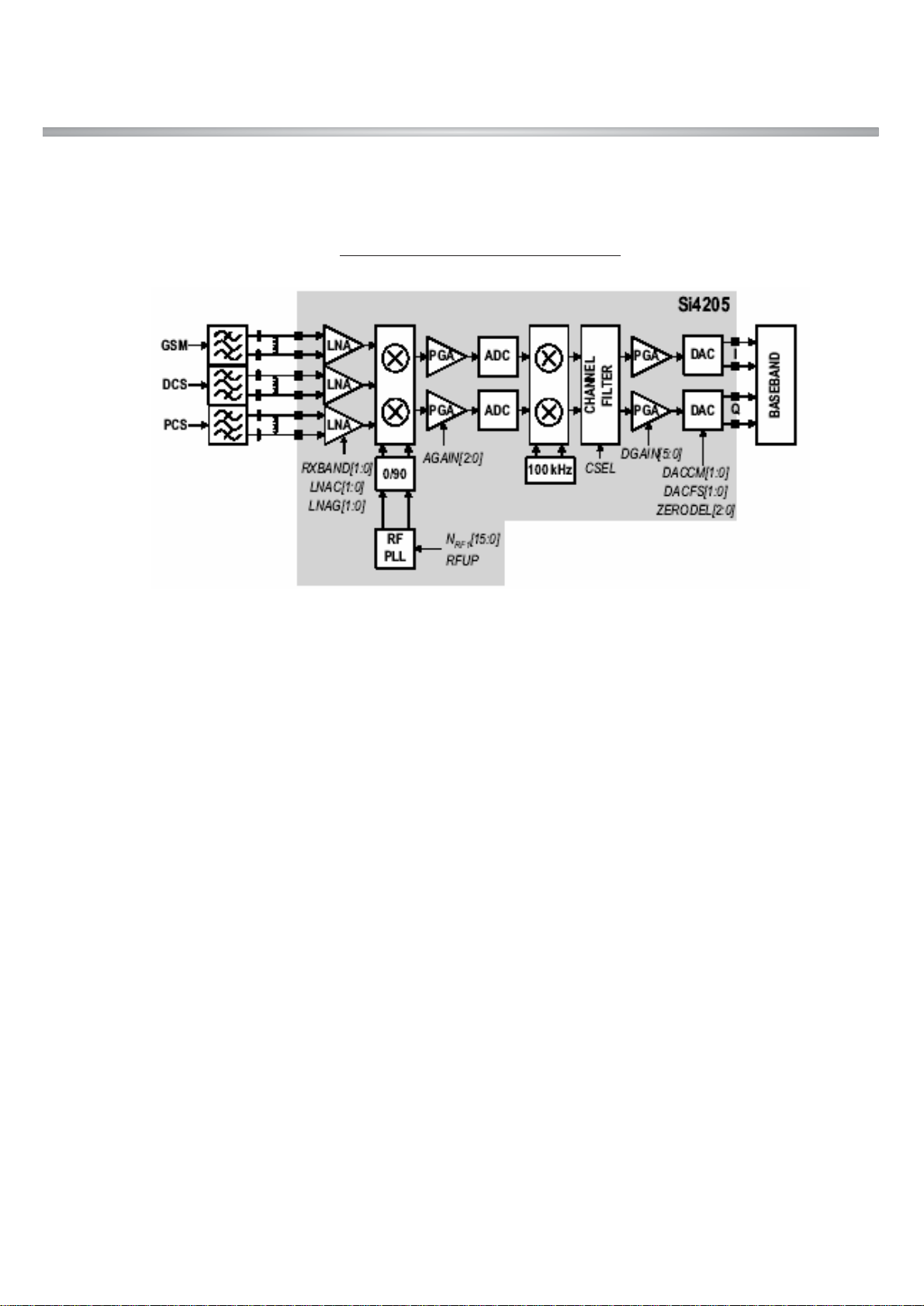
3.1. RF Circuit
The RF parts consist of a transmitter part, a receiver part, a frequency synthesizer part, a voltage
supply part, and a VC-TCXO part.
The AeroI transceiver is composed of one RF chipset, Si4205[U803] which is a triple and quad-band
GSM/GPRS wireless communications.
This device integrated a receiver based on a low IF (100KHz) architecture, a transmitter based on
modulation loop architecture and the synthesizer part with built in VCOs.
The transceiver employed a 3 wire serial interface to allow an external system controller to write the
control registers for dividers, receive path gain, power down setting, and other controls.
3.1.1. Front End Part
RF front end consists of Antenna Switch(FL801), triple-band LNAs integrated in transceiver(U803).
The Received RF signals (GSM850 869 ~ 894MHz, DCS 1805 ~ 1880MHz and PCS 1930 ~
1990MHz) are fed into the antenna or mobile switch. An antenna matching circuit is between the
antenna and the mobile switch. The Antenna Switch(FL801) is used for control the Rx and TX paths.
And, the input signals VC1, VC2 and VC3 of a FL801 are directly connected to baseband controller to
switch either TX or RX path on. Ant S/W module(FL801) is an antenna switch module for dual band
phone. The logic and current is given below Table 1.
The receiver part uses a low-IF receiver architecture that allows for the on-chip integration of the
channel selection filters, eliminating the external RF image reject filters and the IF SAW filter required
in conventional super-heterodyne architecture. The Si4205[U803] integrates three differential input
LNAs that are matched to the 200 ohm balanced-output SAW filters through external LC matching
networks.
3. H/W Circuit Description
VC1 VC2 VC3 Current
GSM850/DCS RX 0 V 0 V 0 V < 0.1 mA
PCS RX 2.85 V 0 V 0 V 10.0 mA max
GSM850 TX 0 V 0 V 2.85 V 10.0 mA max
DCS/PCS 2.85 V 2.85 V 0 V 10.0 mA max
Table 3-1. The Logic and Current

3. H/W Circuit Description
- 16 -
3.1.2. Receiver Part
The Aero I transceiver uses a low-IF receiver architecture which allows for the on-chip integration of
the channel selection filters, eliminating the external RF image reject filters and the IF SAW filter
required in conventional superheterodyne architectures. Compared to a direct-conversion architecture,
the low-IF architecture has a much greater degree of immunity to dc offsets, which can arise from RF
local oscillator (RFLO) self-mixing, nd-order distortion of blockers, and device 1/f noise. This relaxes
the common-mode balance requirements on the input SAW filters, and simplifies PC board design and
manufacturing. Three differential-input LNAs are integrated. The GSM input supports the GSM 850
(869 ~ 894 MHz). The DCS input supports the DCS 1800 (1805 ~ 1880 MHz) band. The PCS input
supports the PCS 1900 (1930 ~ 1990 MHz) band. For quad-band designs, SAW filters for the GSM
850 band should be connected to a balanced combiner which drives the GSM input for both bands.
For dual-band designs using the Si4205DB, the DCS input should be used for either DCS 1800 or
PCS 1900 bands. The LNA inputs are matched to the 150 Ω balancedoutput SAW filters through
external LC matching networks. The LNA gain is controlled with the LNAG[1:0] and LNAC[1:0] bits in
register 05h. A quadrature image-reject mixer downconverts the RF signal to a 100 kHz intermediate
frequency (IF) with the RFLO from the frequency synthesizer. The RFLO frequency is between 1737.8
to 1989.9 MHz, and is internally divided by 2 for GSM 850 mode. The mixer output is amplified with an
analog programmable gain amplifier (PGA), which is controlled with the AGAIN[2:0] bits in register
05h. The quadrature IF signal is digitized with high resolution A/D converters ADCs). The ADC output
is downconverted to baseband with a digital 100 kHz quadrature LO signal. Digital decimation and IIR
filters perform channel selection to remove blocking and reference interference signals. The response
of the IIR filter is programmable to a high selectivity setting (CSEL = 0) or a low selectivity setting
(CSEL = 1). The low selectivity filter has a flatter group delay response which may be desirable where
the final channelization filter is in the baseband chip. After channel selection, the digital output is
scaled with a digital PGA, which is controlled with the DGAIN[5:0] bits in register 05h. The LNAG[1:0],
LNAC[1:0], AGAIN[2:0] and DGAIN[5:0] bits must be set to provide a constant amplitude signal to the
baseband receive inputs. See “AN51: Aero Transceiver AGC Strategy” for more details.
DACs drive a differential analog signal onto the RXIP, RXIN, RXQP, and RXQN pins to interface to
standard analog-input baseband ICs. No special processing is required in the baseband for offset
compensation or extended dynamic range. The receive and transmit baseband I/Q pins can be
multiplexed together into a 4- wire interface. The common mode level at the receive I and Q outputs is
programmable with the DACCM[1:0] bits, and the full scale level is programmable with the DACFS[1:0]
bits in register 12h.
3. H/W Circuit Description
- 17 -
Figure 1. Receiver Part Block Diagram
3. H/W Circuit Description
- 18 -
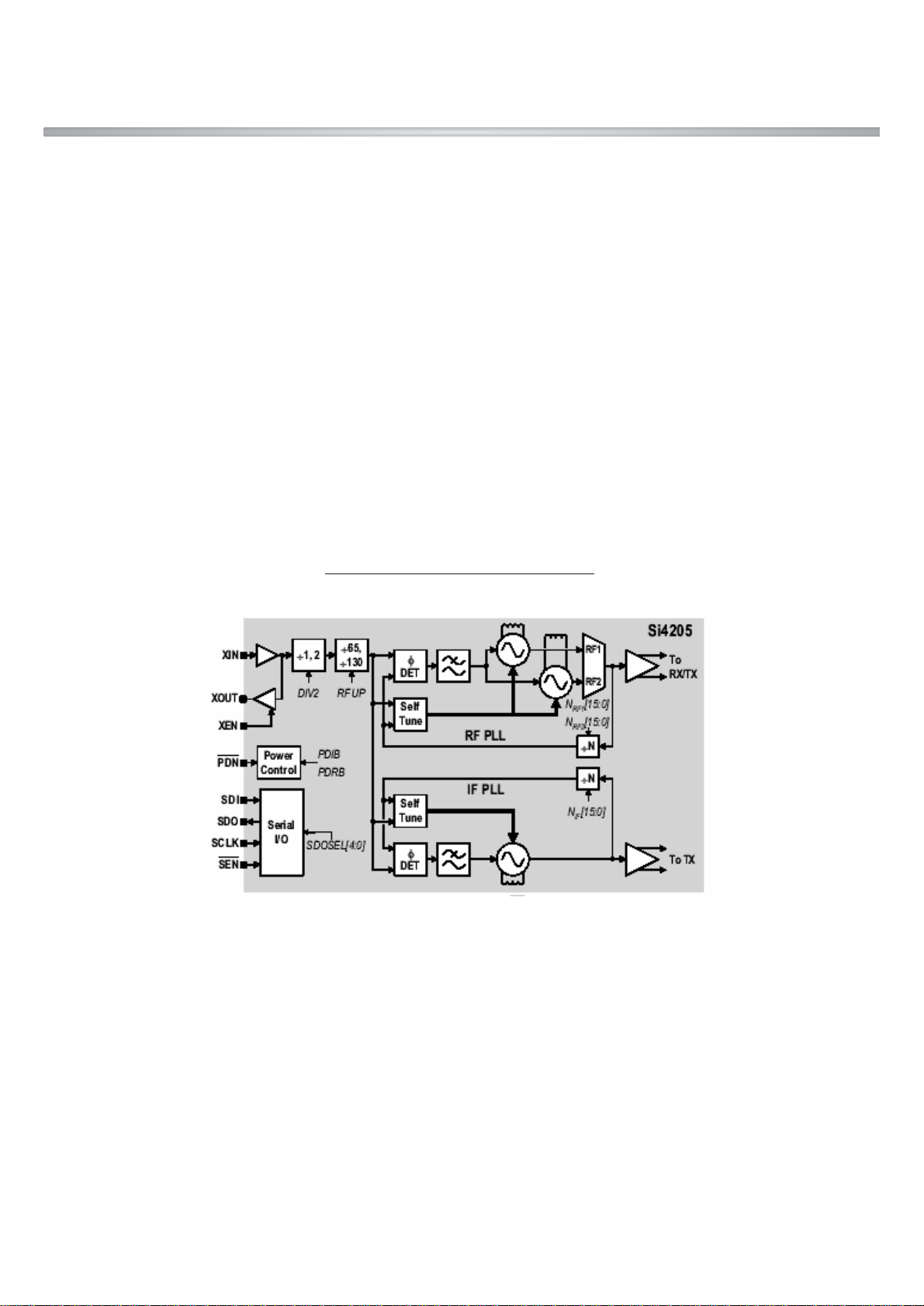
3.1.3. Synthesizer Part
The Aero I transceiver integrates two complete PLLs including VCOs, varactors, resonators, loop
filters, reference and VCO dividers, and phase detectors. The RF PLL uses two multiplexed VCOs.
The RF1 VCO is used for receive mode, and the RF2 VCO is used for transmit mode. The IF PLL is
used only during transmit mode. All VCO tuning inductors are also integrated. The IF and RF output
frequencies are set by programming the N-Divider registers, NRF1, NRF2 and NIF. Programming the
N-Divider register for either RF1 or RF2 automatically selects the proper VCO. The output frequency of
each PLL is as follows:
fOUT = N x fø
The DIV2 bit in register 31h controls a programmable divider at the XIN pin to allow a 26 MHz
reference frequency. For receive mode, the RF1 PLL phase detector update rate (fø) should be
programmed fø = 100 kHz for DCS 1800 or PCS 1900 bands, and fø = 200 kHz for GSM 850. For
transmit mode, the RF2 and IF PLL phase detector update rates are always fø =200 kHz.
Figure 2. Synthesizer Block Diagram
3. H/W Circuit Description
- 19 -
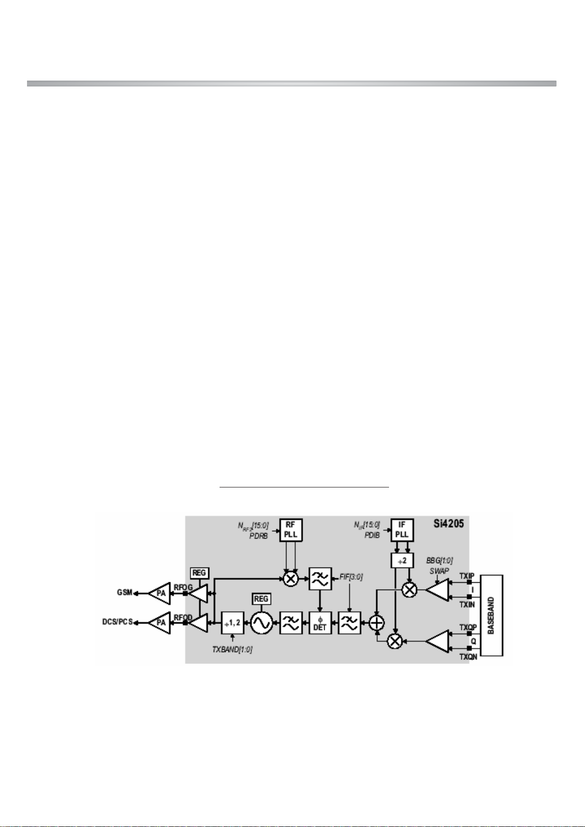
3.1.4. Transmitter Part
The transmit (TX) section consists of an I/Q baseband upconverter, an offset phase-locked loop
(OPLL) and two output buffers that can drive external power amplifiers (PA), one for the GSM 850
(824 to 849 MHz) band and one for the DCS 1800 (1710 to 1785 MHz) and PCS 1900 (1850 to 1910
MHz) bands. The OPLL requires no external duplexer to attenuate transmitter noise or spurious
signals in the receive band, saving both cost and power. Additionally, the output of the transmit VCO
(TXVCO) is a constant-envelope signal that reduces the problem of spectral spreading caused by nonlinearity in the PA A quadrature mixer upconverts the differential in-phase (TXIP, TXIN) and
quadrature (TXQP, TXQN) signals with the IFLO to generate a SSB IF signal that is filtered and used
as the reference input to the OPLL. The IFLO frequency is generated between 766 and 896 MHz and
internally divided by 2 to generate the quadrature LO signals for the quadrature modulator, resulting in
an IF between 383 and 448 MHz.
The OPLL consists of a feedback mixer, a phase detector, a loop filter, and a fully integrated TXVCO.
The TXVCO is centered between the DCS 1800 and PCS 1900 bands, and its output is divided by 2
for the GSM band. The RFLO frequency is generated between 1272 and 1483 MHz. To allow a single
VCO to be used for the RFLO, high-side injection is used for the GSM band, and low-side injection is
used for the DCS 1800 and PCS 1900 bands. The I and Q signals are automatically swapped when
switching bands. Additionally, the SWAP bit in register 03h can be used to manually exchange the I
and Q signals. Low-pass filters before the OPLL phase detector reduce the harmonic content of the
quadrature modulator and feedback mixer outputs. The cutoff frequency of the filters is programmable
with the FIF[3:0] bits in register 04h, and should be set to the recommended settings detailed in the
register description.
Figure 3. Transmitter Block Diagram
3. H/W Circuit Description
- 20 -
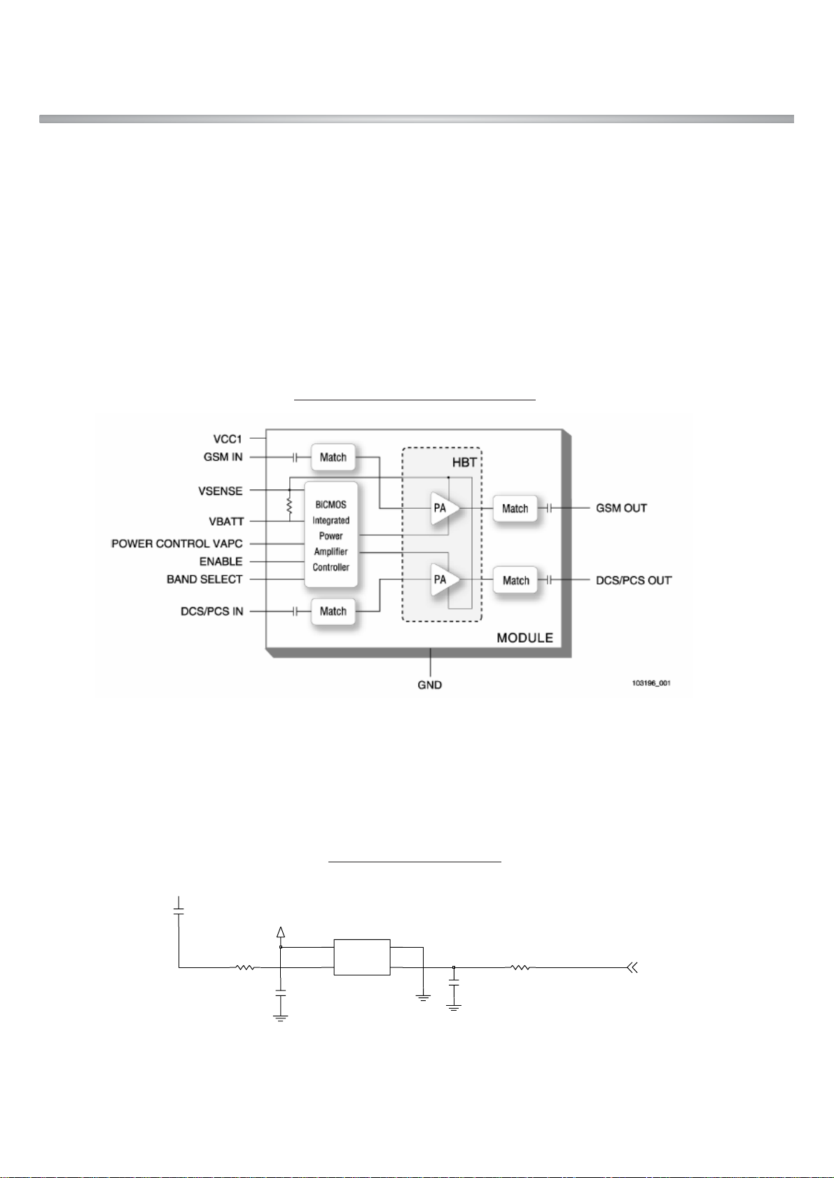
3.1.5. Power Amplifier
The Sky77325 [U804] is a quad-band GSM850/GSM900/DCS/PCS power amplifier module that
incorporates an indirect closed loop method of power control. The indirect closed loop is fully selfcontained and it does not require loop optimization. It can be driven directly from the DAC output in the
baseband circuit. On-board power control provides over 50 dB of control range with an analog voltage
input (Vramp).
Efficiency is 49% at GSM850 and 53% at GSM900, DCS, PCS1900.
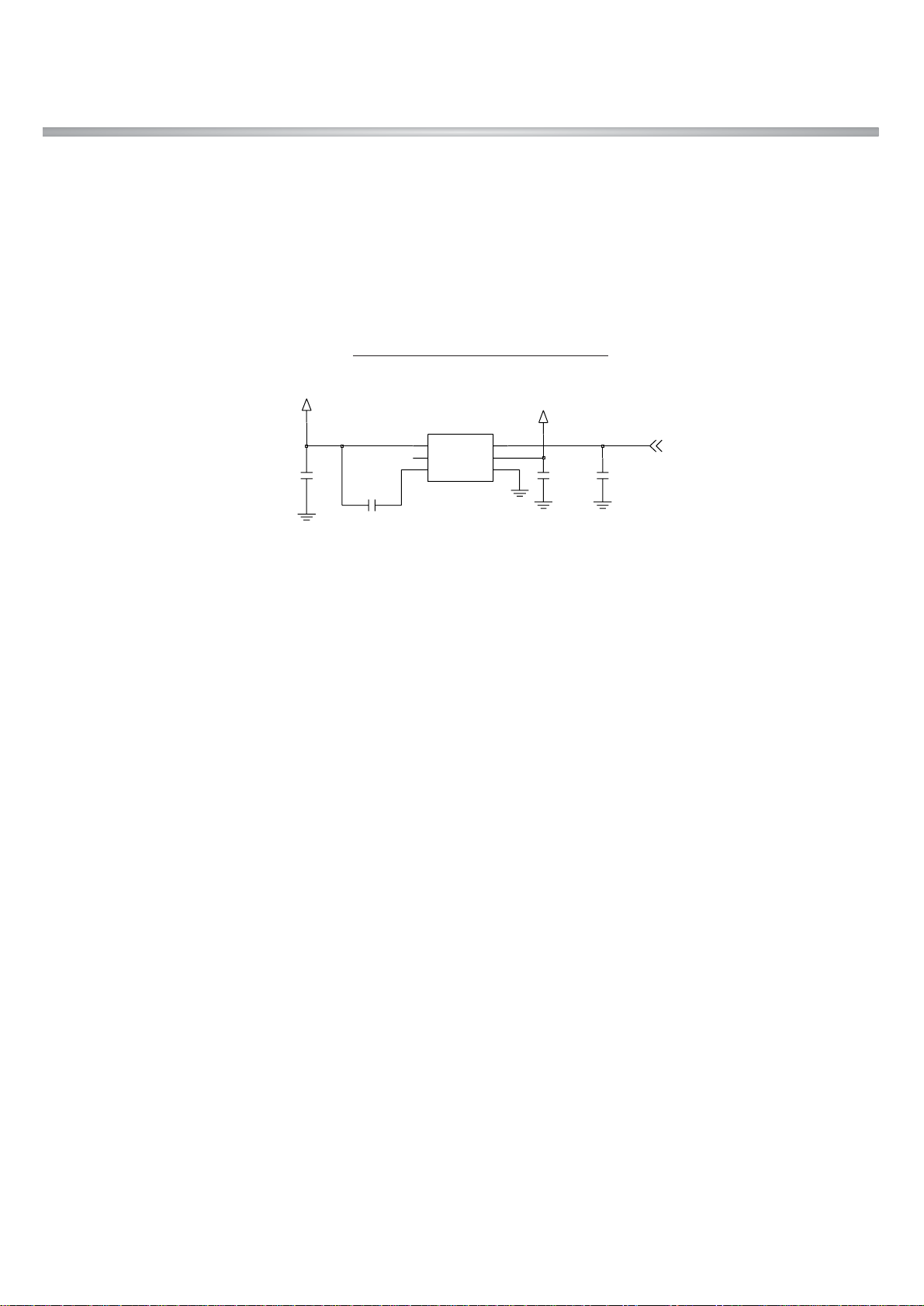
3.1.6. 26 MHz Clock
The 26 MHz clock (X801) consists of a TCXO(Temperature Compensated Crystal Oscillator) which
oscillates at a frequency of 26 MHz. It is used within the Si4205 RF Main Chip, BB Analog chip-set
(IOTA), Digital chip-set(Calypso G2).
Figure 4. Power Amp Block Diagram
RF2.85V
1.5K
R824
100
R823
10p
C838
2.2u
C839
100p
C835
X801
26MHz
GND
2
OUT
3
4
VCC
1
VCONT
AFC
Figure 5. VC-TCXO Circuit
3. H/W Circuit Description
- 21 -
3.1.7. Power Supplies and Control Signals
An external regulator (U805) is used to provide DC power to RF part. Every RF component except
power amp module uses this external regulator.
(1608) (1608)
470p
C849
VBAT
3
6
_SD
ADP3330
U805
4
GND
2
IN
5
NR
OUT
1
_ERR
RF2.85V
C848
10p
0.47u
C846
C847
2.2u
RF_EN
Figure 6. External regulator Circuit
3. H/W Circuit Description
- 22 -
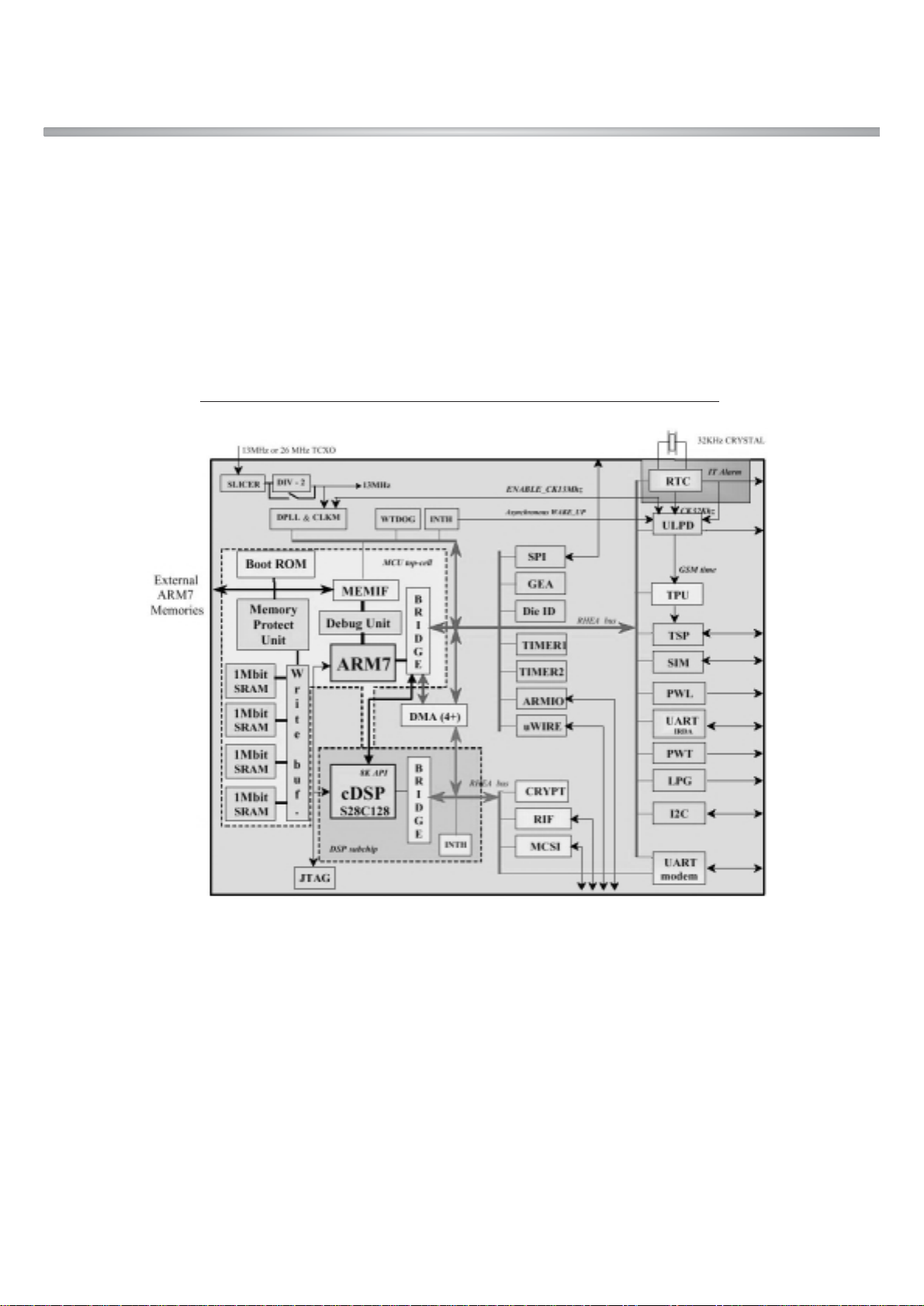
3.2. Digital Baseband(DBB) Processor
O Circuito Receptor, localizado no CX74017, contém todos os circuitos completamente ativados,
corrente total do receptor com exceção dos filtros RF SAW discretos da extremidade frontal. O sinal
filtrado e amplificado é convertido em um mixer RF para saída banda base. O caminho de recepção é
fornecido por um filtro interno de canal.
3.2.1. General Description
CALYPSO is a chip implementing the digital base-band processes of a GSM/GPRS mobile phone.
This chip combines a DSP sub-chip (LEAD2 CPU) with its program and data memories, a Micro- Controller core with emulation facilities (ARM7TDMIE), internal 8Kb of Boot ROM memory, 4M bit
SRAM memory, a clock squarer cell, several compiled single-port or 2-ports RAM and CMOS gates.
The chip will fully support the Full-Rate, Enhanced Full-Rate and Half-Rate speech coding.
CALYPSO implements all features for the structural test of the logic (full-SCAN, BIST, PMT, JTAG
boundary-SCAN).
Figure 7. Top level block diagram of the Calypso G2(HERCROM400G2)

3. H/W Circuit Description
- 23 -
3.2.2. Block Description
CALYPSO architecture is based on two processor cores ARM7 and DSP using the generic RHEA bus
standard as interface with their associated application peripherals.
CALYPSO is composed from the following blocks:
• ARM7TDMIE : ARM7TDMI CPU core
• DSP subchip
• ARM peripherals:
General purpose peripherals
• ARM Memory Interface for external RAM, Flash or ROM
• 4 Mbit Static RAM with write-buffer
Application peripherals
• ARM General purposes I/O with keyboard interface and two PWM modulation signals
• UART 16C750 interface (UART_IRDA) with
- IRDA control capabilities (SIR)
- Software flow control (UART mode).
• UART 16C750 interface (UART_MODEM) with
- hardware flow protocol (DCD, CTS/RTS)
- autobaud function
• SIM Interface.
• TPU(Time Processing Unit) : Processing for GSM time base
• TSP(Time Serial Port) : GSM data interface with RF and ABB
Memory Interface : External/Internal Memory Interface
nCS0 : FLASH1, 16bit access, 4 wait state
nCS1 : FLAHS2, 16bit access, 4 wait state
nCS2 : Ext SRAM, 16bit access, 4 wait state
nCS3 : Main LCD(16bit access), 8 wait state
nCS4 : MIDI(8bit access), SUB-LCD(8bit access) addressing, 5 wait state
nCS6 : Int SRAM, 32bit access, 0 wait state
* Calypso is internally 52MHz machine (20ns machine cycle), so it requires 4 wait-state for 80ns
access(20*5 = 100 ns).
3. H/W Circuit Description
- 24 -
3.2.3. External Devices connected to memory interface
3.2.4. RF Interface (TPU, TSP block)
Calypso uses this interface to control IOTA_CS(ABB Processor) and AERO(RF Processor) with GSM
Time Base.
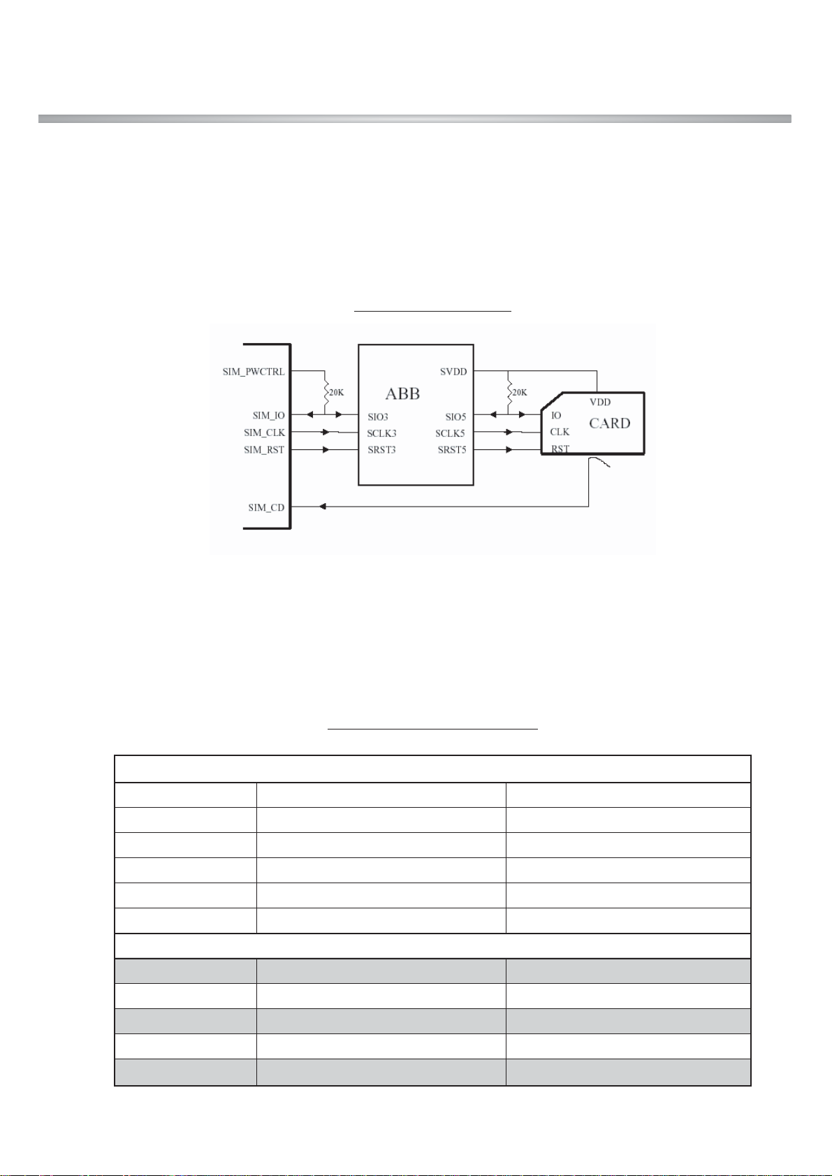
3.2.5. SIM interface
SIM interface scheme is shown in (Figure 10).
SIM_IO, SIM_CLK, SIM_RST ports are used to communicate DBB with ABB and the Charge Pump in
ABB enables 3V SIM operation.
SIM Interface
] SIM_CLK ------------- SIM card reference clock
] SIM_RST ------------- SIM card async/sync reset
] SIM_IO ---------------- SIM card bidirectional reset
Device Name Maker Write Read
Access Time Access Time
FLASH AM50DL128CH AMD 70ns 70ns
SRAM AM50DL128CG70I AMD 70ns 70ns
LCD NM186TB-2 NEODIS 130ns 50ns
Melody IC YMU762 Yamaha 50ns 80ns
Table 3-2. Memory interface
TSP (Time Serial Port)
Resource Interconnection Description
TSPDO ABB & RF main Chip Control Data
TSPEN0 ABB ABB Control Data Enable Signal
TSPEN1 RF main Chip RF Control Data Enable Signal
TPU (Time Processing Unit) Parallel Port
TSPACT00 RESET_RF RF main Chip Reset Signal
TSPACT05 PA_ON Power Amp ON signal
Table 3-3. RF Interface Spec.
3. H/W Circuit Description
- 25 -
] SIM_PWCTRL ------ SIM card power activation
] SIM_RnW ------------ SIM card data line direction
] SIM_CD --------------- SIM card presence detection
3.2.6. UART Interface
L1150 have two UART Drivers as follow :
- UART1 : Hardware Flow Control / Fax&Data Modem
- UART2 : Handsfree Control / SW trace or IrDA Modem
Figure 10. SIM Interface
UART MODEM (UART1)
Resource Name Remark
TX_MODEM TXD Transmit Data
RX_MODEM RXD Receive Data
CTS_MODEM CTS Clear To Send
RTS_MODEM RTS Request To Send
GPIO 3 DSR Data Set Ready
UART IrDA (UART2)
TXIR_IRDA TXIR_IRDA Infra-Red Transmit Pulse
TX_IRDA TX Transmit Data(UART2)
RXIR_IRDA RXIR_IRDA Infra-Red Receive Pulse
RX_IRDA RX Receive Data(UART2)
SD_IRDA SD_IRDA IRDA transceiver ShutDown Mode
Table 3-4. UART Interface Spec.
3. H/W Circuit Description
- 26 -
3.2.7. GPIO map
In total 16 allowable resources, L1150 is using 13 resources except 3 resources dedicated to SIM and
Memory. L1150 GPIO(General Purpose Input/Output) Map, describing application, I/O state, and
enable level, is shown in below table.
I/O # Application I/O Resource State Inactive State Active State
I/O (0) FOLDER I GPIO HIGH (Open) LOW (Closed)
I/O (1) MELODY_INT I GPIO HIGH (No int) LOW (Interrupt)
I/O (2) SPK_EN O GPIO
LOW HIGH
(REC path) (Speaker phone)
I/O (3) DSR I GPIO
HIGH LOW
(No Data Ready ) (Data Ready)
I/O (4) LCD_BACKLIGHT O GPIO LOW (OFF) HIGH (note1)
I/O (5) SIM_PWCTL O SIM
I/O (6) BCLKX O GPIO LOW (OFF)
HIGH
(LDO Output ON)
I/O (7) LCD_RESET O GPIO HIGH (Normal) LOW (Reset)
I/O (8) IFMODE O GPIO
I/O (9) CAM_HOLD/PCM_TX O GPIO
LOW HIGH
(CAM mode) (LCD path bypass)
I/O (10) INDLED_R /PCM_RX I GPIO
I/O (11) INDLED_G /PCM_CLK I/O GPIO
I/O (12) LCD_ID/ PCM_SYNC I/O GPIO
I/O (13) HANDSFREE I GPIO HIGH LOW (HF detected)
I/O (14) NBHE O MEMORY
I/O (15) NBLE O MEMORY
Table 3-5. GPIO Map Table
3. H/W Circuit Description
- 27 -
3.3. Analog Baseband(ABB) Processor
3.3.1. General Description
IOTA is Analog Baseband (ABB) Chip supports GSM900, DCS1800, PCS1900, GPRS Class 10 with
Digital Baseband Chip(Calypso G2). IOTA processes GSM modulation/demodulation and power
management operations.
Block Description
- Audio Signal Processing & Interface
- Baseband in-phase(I), quadrature(Q) Signal Processing
- RF interface with DBB (time serial port)
- Supply voltage regulation
- Battery charging control
- Switch ON/OFF
- 3V SIM card Interface
- 4 internal & 4external ADC channels
Figure 11. Top level block diagram of the IOTA(TWL3014CGGM)
3. H/W Circuit Description
- 28 -
3.3.2. Audio Signal Processing & Interface
Audio signal processing is divided Uplink path and downlink path.
The uplink path amplifies the audio signal from MIC and converts this analog signal to digital signal
and then transmit it to DBB Chip. This transmitted signal is reformed to fit in GSM Frame format and
delivered to RF Chip. MICBIAS is 2.0Vlevel.
The downlink path amplifies the signal from DBB chip and outputs it to Receiver (or Speaker).
3.3.3. Audio uplink processing
The microphone is soldered to the main PCB. The uplink signal is passed to MICIP and MICIN pins of
IOTA.
The MICBIAS voltage is supplied from IOTA(dedicated mode only). When the headset is inserted,
ADC value of HOOK_DETECT(IO6) terminal is between 20 to 150 (decimal value). On detecting this,
Calypso makes IOTA switches the MIC amplifier path from main to auxiliary.
Figure 12. Audio Interface Block Diagram
3. H/W Circuit Description
- 29 -
3.3.4. Audio downlink processing
The downlink signal is passed from EARP and EARN pins of IOTA. When the headset is inserted and
Calypso detects ‘Jack pluged state’ from HOOK_DETECT terminal, Calypso makes IOTA switches the
downlink path from ‘EARP’ and ‘EARN’ to auxiliary outputs(‘AUXOP’ and ‘AUXON’ or ‘HSO’).
Figure 13. Uplink Path
Figure 14. Downlink Path
 Loading...