

LG L-06A Service Manual

Service Manual Model : L-06A
Internal Use Only
Service Manual
L-06A
Date: July, 2009 / Issue 1.0

Table Of Contents
1. INTRODUCTION ...............................................5
1.1 Purpose ......................................................................5
1.2 Regulatory Information .................................................5
2. PERFORMANCE ...............................................7
2.1 System Overview .........................................................7
2.2 Usable environment .....................................................8
2.3 wireless characteristic .................................................9
2.4 Current consumption .................................................15
2.5 RSSI (Call (W2100 0dBm /EGSM Power level 19) :
Cell Power) ...............................................................15
2.6 Battery Bar ................................................................16
2.7 Sound pressure Level ................................................17
2.8 SAR characteristic .....................................................18
3. TECHNICAL BRIEF .........................................19
3.1 General Description ...................................................19
3.2 GSM Mode ................................................................22
3.3 UMTS Mode ..............................................................26
3.4 LO Phase-locked Loop ...............................................31
3.5 Off-chip RF Components ............................................32
3.6 Digital Baseband(DBB/MSM7200A) ............................47
3.7 Modem subsystem ....................................................50
3.8 Power Block ..............................................................63
3.9 Memory interface ......................................................73
3.10 H/W Sub System .....................................................75
3.11 Main Features .........................................................93
4. TROUBLE SHOOTING ................................... 103
4.1 Checking VCXO Block ..............................................103
4.2 Checking Ant. SW Module Block ...............................105
4.3 Checking UMTS Block ..............................................107
4.4 Checking GSM Block ...............................................116
4.5 Power ON Troubleshooting .......................................120
4.6 Charger Troubleshooting ..........................................123
4.7 USB Troubleshooting ................................................125
4.8 SIM Detect Troubleshooting ......................................128
4.9 Keypad Backlight Troubleshooting .............................135
4.10 Folder Close / Open Troubleshooting .......................136
4.11 Swivel Close / Open Troubleshooting .......................137
4.12 Main LCD Troubleshooting......................................138
4.13 Receiver Path ........................................................139
4.14 Headset path.........................................................141
4.15 Speaker phone path ..............................................142
4.16 Main microphone ..................................................144
4.17 Headset microphone ..............................................146
4.18 Vibrator .................................................................148
4.19 1-seg ...................................................................150
4.20 3AXIS Sensor ........................................................152
4.21 Touch Sensor ........................................................153
4.22 SD card operation..................................................155
4.23 Light Sensor Operation ..........................................158
4.24 FeliCa ...................................................................159
5. Downloading .............................................. 161
5.1 Introduction .............................................................161
5.2 Downloading Procedure ...........................................162
5.3 Troubleshooting Download Errors ..............................177
5.4 Caution ...................................................................184
6. BLOCK DIAGRAM ........................................ 185
6.1 GSM & UMTS RF Block ............................................185
6.2 RF Component ........................................................186
7. CIRCUIT DIAGRAM ...................................... 193
8. BGA Pin Map ..............................................203
9. PCB LAYOUT ...............................................213
10. Calibration & RF Auto Test Program
(Hot Kimchi) ............................................. 221
10.1 Confi guration of HOT KIMCHI .................................221
10.2 How to use HOT KIMCHI.........................................223
11. EXPLODED VIEW & REPLACEMENT
PART LIST ................................................225
11.1 EXPLODED VIEW ...................................................225
11.2 Replacement Parts ................................................227
11.3 Accessory ............................................................. 262
Copyright © 2009 LG Electronics. Inc. All right reserved.
Only for training and service purposes
- 3 -
LGE Internal Use Only

LGE Internal Use Only Copyright © 2009 LG Electronics. Inc. All right reserved.
- 4 -
Only for training and service purposes

1. INTRODUCTION
1.1 Purpose
This manual provides the information necessary to repair, calibration, description and download the
features of this model.
1.2 Regulatory Information
A. Security
Toll fraud, the unauthorized use of telecommunications system by an unauthorized part (for example,
persons other than your company’s employees, agents, subcontractors, or person working on your
company’s behalf) can result in substantial additional charges for your telecommunications services.
System users are responsible for the security of own system. There are may be risks of toll fraud
associated with your telecommunications system. System users are responsible for programming and
configuring the equipment to prevent unauthorized use. The manufacturer does not warrant that this
product is immune from the above case but will prevent unauthorized use of common-carrier
telecommunication service of facilities accessed through or connected to it. The manufacturer will not
be responsible for any charges that result from such unauthorized use.
B. Incidence of Harm
If a telephone company determines that the equipment provided to customer is faulty and possibly
causing harm or interruption in service to the telephone network, it should disconnect telephone
service until repair can be done. A telephone company may temporarily disconnect service as long as
repair is not done.
C. Changes in Service
A local telephone company may make changes in its communications facilities or procedure. If these
changes could reasonably be expected to affect the use of the phones or compatibility with the net
work, the telephone company is required to give advanced written notice to the user, allowing the user
to take appropriate steps to maintain telephone service.
D. Maintenance Limitations
Maintenance limitations on the phones must be performed only by the manufacturer or its authorized
agent. The user may not make any changes and/or repairs expect as specifically noted in this manual.
Therefore, note that unauthorized alternations or repair may affect the regulatory status of the system
and may void any remaining warranty.
1. INTRODUCTION
Copyright © 2009 LG Electronics. Inc. All right reserved.
Only for training and service purposes
- 5 -
LGE Internal Use Only

1. INTRODUCTION
E. Notice of Radiated Emissions
This model complies with rules regarding radiation and radio frequency emission as defined by local
regulatory agencies. In accordance with these agencies, you may be required to provide information
such as the following to the end user.
F. Pictures
The pictures in this manual are for illustrative purposes only; your actual hardware may look slightly
different.
G. Interference and Attenuation
A phone may interfere with sensitive laboratory equipment, medical equipment, etc. Interference from
unsuppressed engines or electric motors may cause problems.
H. Electrostatic Sensitive Devices
ATTENTION
Boards, which contain Electrostatic Sensitive Device (ESD), are indicated by the sign.
Following information is ESD handling:
• Service personnel should ground themselves by using a wrist strap when exchange system boards.
• When repairs are made to a system board, they should spread the floor with anti-static mat which is
also grounded.
• Use a suitable, grounded soldering iron.
• Keep sensitive parts in these protective packages until these are used.
• When returning system boards or parts like EEPROM to the factory, use the protective package as
described.
LGE Internal Use Only Copyright © 2009 LG Electronics. Inc. All right reserved.
- 6 -
Only for training and service purposes
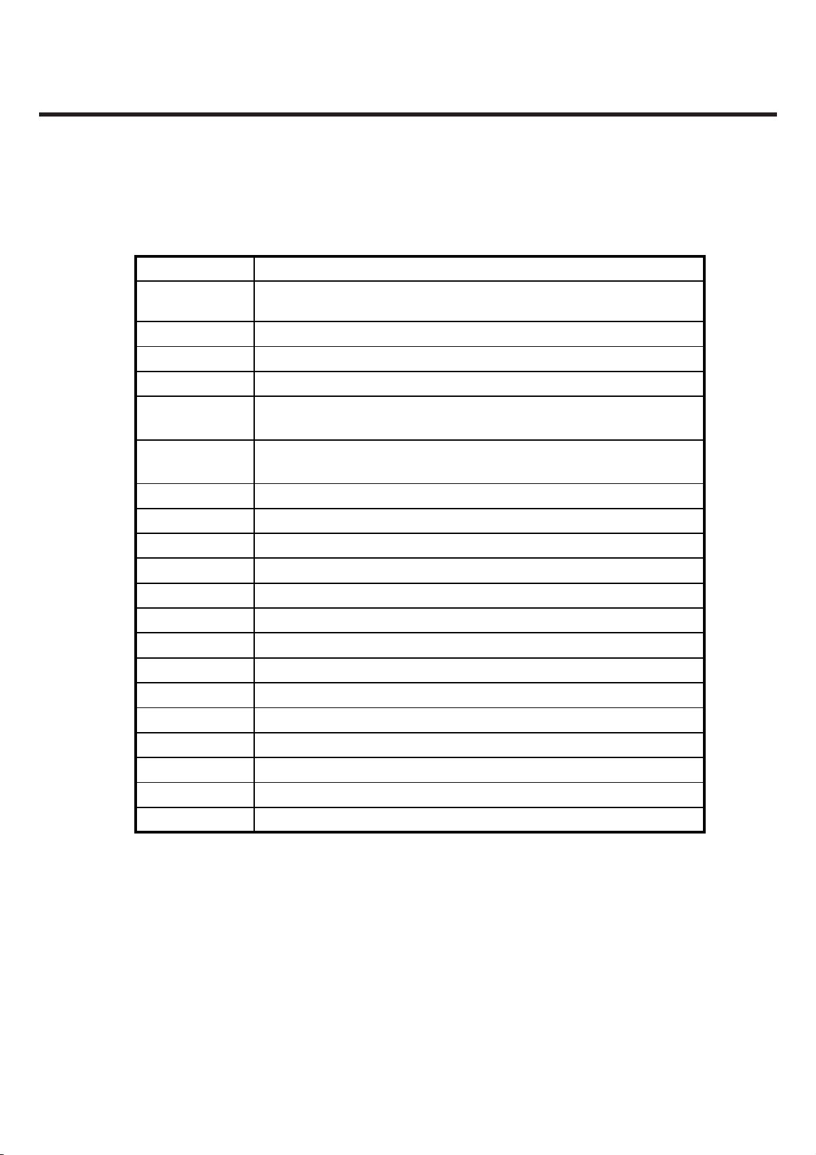
2. PERFORMANCE
2.1 System Overview
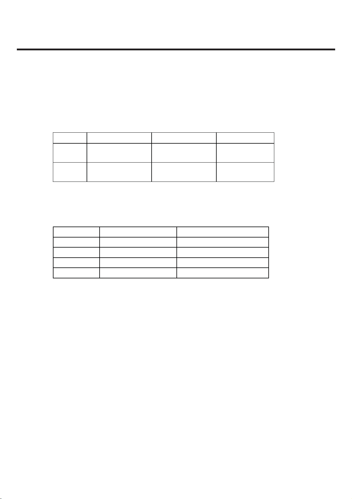
2. PERFORMANCE
SpecificationItem
External form
Call time
Wait time
WCDMA2100,800/GSM900/DCS1800/PCS1900 Swivel type Dual mode mobile
phone
110X52X15.4 [mmXmmXmm]Size
about 131g (Battery included)Weight
3.7V, 900mAh Li-IonPower
Over 180 min. (WCDMA, Tx=10 dBm, Voice) 260 mA
Over 140 min (GSM900, Tx= greatest output, Voice) 330 mA
Over 300 hrs (WCDMA only mode, DRX = 2.56s) (under 3.0 mA)
Over 250 hrs (GSM, Paging period = 5) (under 3.5 mA)
O
In 3 hours ( 0
IntennaAntenna
3.0"(480x800 Dot), 262K TFT Color LCDMain LCD
White LED Back LightMain LCD BL
Yes (10 pie coin type)Vibrator
Yes LED Indicator
Yes (SMD type)C-Mic
Yes (18X10)Receiver
~ 40O )Charging time
Yes (18X10)Loud Speaker
Yes (10 pin Japan standard)Ear phone jack
Yes (3.0V/1.8V)SIM Socket
Push Type Side Key(+,-)Volume Key
Push TypeVoice Key
ARIB Type A (10 pin + RF coaxial)I/O Connector
Copyright © 2009 LG Electronics. Inc. All right reserved.
Only for training and service purposes
- 7 -
LGE Internal Use Only
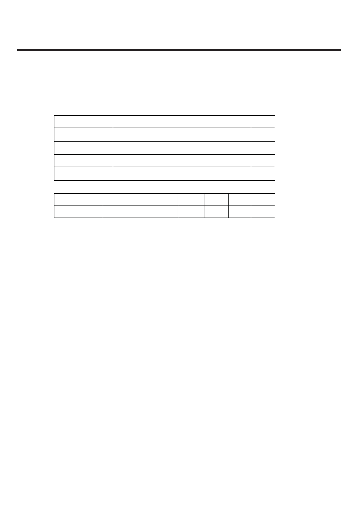
2. PERFORMANCE
g
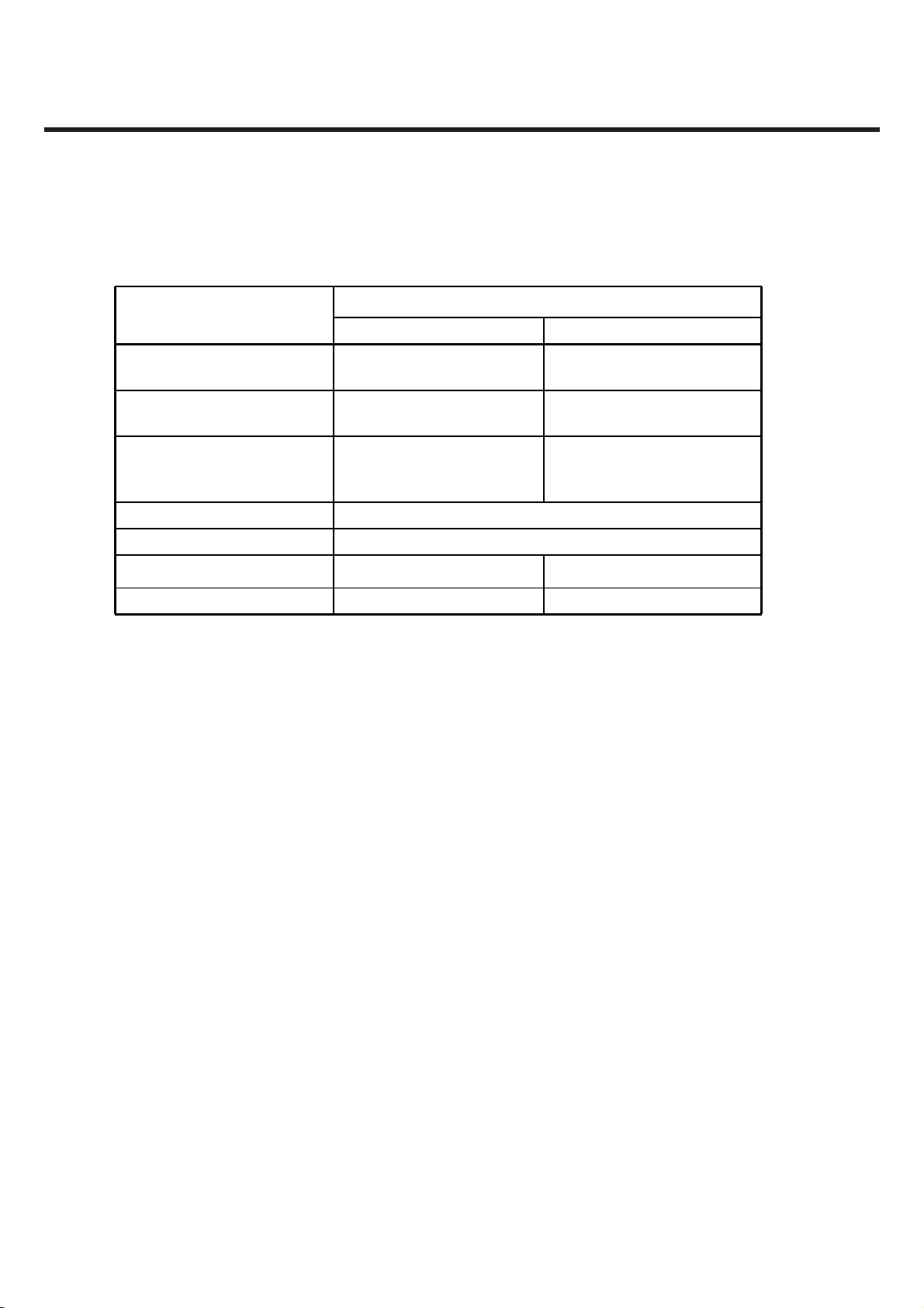
2.2 Usable environment
1) Phone using environment
Item
Using Voltage V3.7 (Typ) ( Shut Down: 3.28)
Using Temp.
Store Temp.
humidity 40 ~ 85 %
2) Using environment(Accessory)
Item Unit
Input power
* TA support FOMA common adapter.
UnitSpec.
-20 ~ + 60
-30 ~ + 85 ℃
Spec.
Using power 100 220 240
MaxTyp.Min
℃
Vac
LGE Internal Use Only Copyright © 2009 LG Electronics. Inc. All right reserved.
- 8 -
Only for training and service purposes
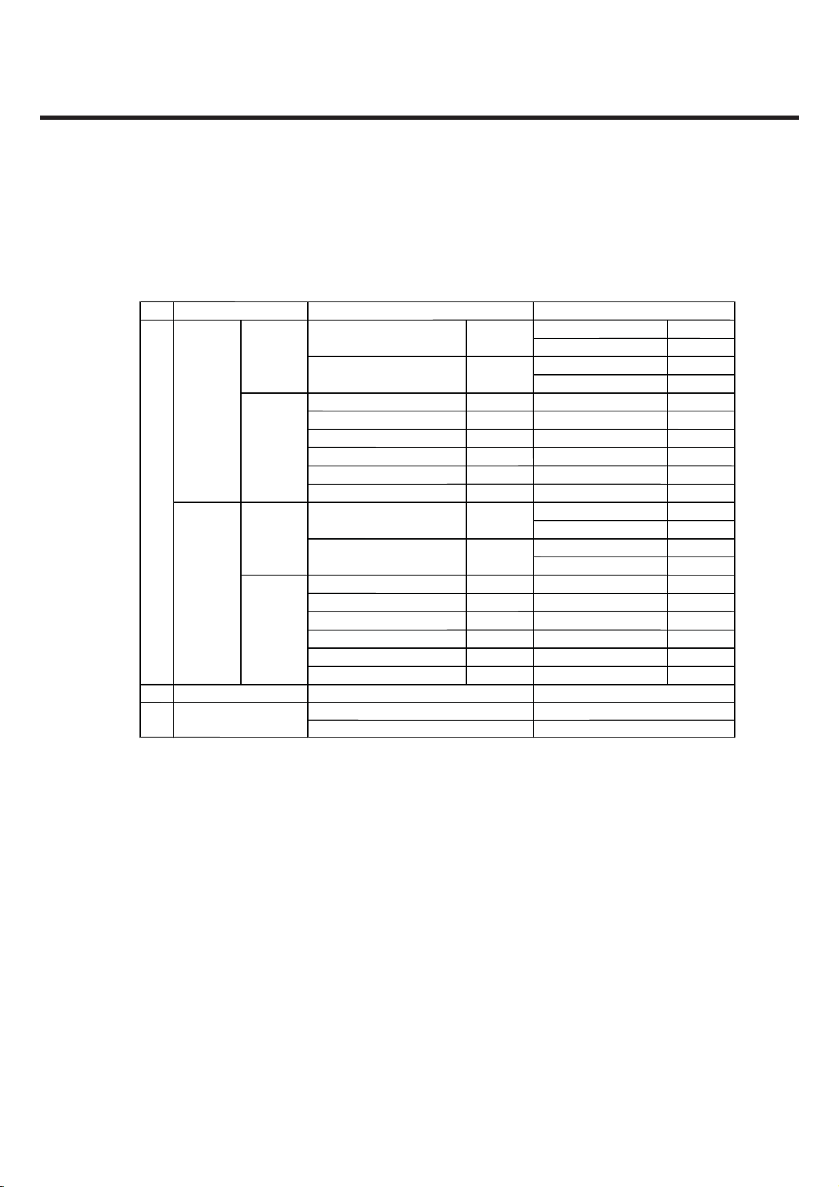
2. PERFORMANCE
2.3 wireless characteristic
wireless characteristic follows GSM Approval examination Specification(ETSI EN 300 607 11.10)
1) Frequency characteristic of transmission part - GSM Mode
NO
1
2
3 Phase Error
Item
Conducted MS
Spurious
Emission -39dBm
Radiated -36dBm
Spurious
Emission
allocated
Channel
Idle Mode
MS
allocated
Channel
Idle Mode
Frequency Error
100k ~ 1GHz -39dBm
1G ~ 12.75GHz -33dBm
100k ~ 880MHz 100k ~ 880MHz
880M ~ 915MHz 880M ~ 915MHz
915M ~ 1000Mz 915M ~ 1000MHz
1G ~ 1.71GHz 1G ~ 1.71GHz
1.71G ~ 1.785GHz 1.71G ~ 1.785GHz
1.785G ~ 12.75GHz 1.785G ~ 12.75GHz
30M ~ 1GHz -36dBm
1G ~ 4GHz -30dBm
30M ~ 880MHz 30M ~ 880MHz
880M ~ 915MHz
915M ~ 1000MHz 915M ~ 1000MHz
1G ~ 1.71GHz 1G ~ 1.71GHz
1.71G ~ 1.785GHz
1.785G~ 4GHz 1.785G~ 4GHz
??
0.1ppm
?5?
(RMS)
?20?
(PEAK)
GSM DCS
9k ~ 1GHz
1G ~ 1710MHz
1710M ~ 1785MHz
1785M ~ 12.75GHz
-60dBm -60dBm
-62dBm -62dBm
-60dBm -60dBm
-50dBm -50dBm
-56dBm -56dBm
-50dBm -50dBm
30M ~ 1GHz
1G ~ 1710MHz
1710M ~ 1785MHz
1785M ~ 4GHz
-57dBm
-59dBm
-57dBm
-47dBm
-53dBm
-47dBm
880M ~ 915MHz
1.71G ~ 1.785GHz
??
0.1ppm
?5?
(RMS)
?20?
(PEAK)
-39dBm
-33dBm
-33dBm
-30dBm
-36dBm
-30dBm
-57dBm
-59dBm
-57dBm
-47dBm
-53dBm
-47dBm
Copyright © 2009 LG Electronics. Inc. All right reserved.
Only for training and service purposes
- 9 -
LGE Internal Use Only
2. PERFORMANCE
1) Frequency characteristic of transmission part -GSM Mode(continued)
NO
4
5
7 Intermodulation attenuation
8 Trans mitter Output Powe r
9
Item
Frequency Error Under
Multipath and Interference
Condition
Due to
modulation
Output RF
Spectrum
Due to
Switching
tran si ent
Burst tim ing Mas k IN
3dB below reference sensitivity 3dB below reference sensitivity
RA250: ±200Hz RA250: ±250Hz
HT100: ±100Hz HT100: ±250Hz
TU50: ±100Hz TU50: ±150Hz
TU3: ±150Hz TU1.5: ±200Hz
0 ~ 100kHz 0 ~ 100kHz
200kHz 200kHz
250kHz 250kHz
400kHz 400kHz
600 ~ 1800kHz 600 ~ 1800kHz
1800 ~ 3000kHz 1800 ~ 6000kHz
3000 ~ 6000kHz ³ 6000kHz
³ 6000kHz
400kHz 400kHz
600kHz 600kHz
1200kHz 1200kHz
1800kHz 1800kHz
Power
control Power
Level (dBm) Level (dBm) (dB)
533 0 30 ±3
631 1 28 ±3
729 2 26 ±3
827 3 24 ±3
925 4 22 ±3
10 23 5 20 ±3
11 21 6 18 ±3
12 19 7 16 ±3
13 17 8 14 ±3
14 15 9 12 ±4
15 13 10 10 ±4
16 11 11 8 ±4
17 9 12 6 ±4
18 7 13 4 ±4
19 5 14 2 ±5
GSM DCS
-
Tolerance
+0.5dB +0.5dB
-30dB -30dB
-33dB -31dB
-60dB -33dB
-66dB -60dB
-69dB -60dB
-71dB -73dB
-77dB
-19dB -22dB
-21dB -24dB
-21dB -24dB
-24dB -27dB
Frequency offset
Intermodulation product should be
Less than 55dB below the level of
Wanted signal
Power
control Power Tolerance
(dB)
±3
±3
±3
±3
±3
±3
±3
±3
±3
±3
±3
±5
±5
±5
±5
15 0 ±5
Mask IN
800kHz
LGE Internal Use Only Copyright © 2009 LG Electronics. Inc. All right reserved.
- 10 -
Only for training and service purposes
1) Frequency characteristic of transmission part -WCDMA Mode
35-15*(Δf-2.5) dBc @Δf= 2.5~3.5MHz
2. PERFORMANCE
NO
1 Maximum Output Power
Item
Standard
Class3: +24 dBm (+1/-3dB)
Class4: +21dBm(±2dB)
2 Frequency Error ± 0.1ppm
3 Open Loop Power control in uplink ± 9dB
In
Adjust output(TPC command)
cmd 1dB 2dB 3dB
+1 +0.5/1.5 +1/3 +1.5/4
0 -0.5/+0.5 -0.5/+0.5 -0.5/+0.5
-1 -0.5/-1.5 -1/-3 -1.5/-4
4 Inner Loop Power control in uplink
group(10equal command group)
+1 +8/+12 +16/+24
5 Minimum Output Power -50 dBm
Out-of-synchronization handling
6
of output power
Qin/Qout:DPCCH quality levels
Toff@ DPCCH/Ior:-22->-28dB
Ton@ DPCCH/ Ior:-24->-18dB
under
@normal, ±12dB @extreme
(3.84MHz)
Under (3.84MHz)
7 Transmit OFF Power -56 dBm
8 Transmit ON/OFF Time Mask
±25us
PRACH,CPCH, uplink c ompressed mode
±25us
9 Change of TFC
power varies according to the data rate
DTX: DPCH off
(minise interference between UE)
Power setting in uplink
10 ±3dB
compressed
In
11 Occupied Bandwidth(OBW) 5 MHz
-
-35-1*(Δf-3.5) dBc @Δf=3.5~7.5MHz,1M
12 Spectrum emission Mask
-39 10*(Δf-7.5) dBc @Δf=7.5~8.5MHz,1M
-49 dBc @Δ f=8.5~12.5MHz,1M
Adjacent Channel Leakage Ratio
13
(ACLR)
33dB
43dB
(3.84M)
Under (3.84M)
( after14slots transmission gap)
(99% )
Under (99%)
@5MHz , ACP>-50dBm
over
@10MHz , ACP>-50dBm
over
,
Copyright © 2009 LG Electronics. Inc. All right reserved.
Only for training and service purposes
- 11 -
LGE Internal Use Only
2. PERFORMANCE
1) Frequency characteristic of transmission part -WCDMA Mode(continued)
-36 dBm @f=9~150KHz, 1k BW
WCDMA
2100, 800
14
Spurious Emission
*:addition requirement
WCDMA
2100
WCDMA
800
15 Transmit Intermodulation
16 Error Vector Magnitude(EVM)
17 Peak code domain error
-36 dBm @f=150KHz~30MHz, 10k
-36 dBm @f=30~1000MHz, 100k
-30 dBm @f=1~12.75GHz, 1M
-41 dBm* @1893.5~1919.6MHz, 300k
-67 dBm* @925~935MHz, 100k
-79 dBm* @935~960MHz, 100k
-71 dBm* @1805~1880MHz, 100k
-60 dBm* @869~894MHz, 3.84M
-60 dBm* @1930~1990MHz, 3.84M
-60 dBm* @2110~2155MHz, 3.84M
-31 dBc @5MHz,Interferer -40dBc
-41 dBc @10MHz,Interferer -40dBc
under 17.5%
17.5 %
( >-20dBm)
(@12.2k, 1DPDCH+1DPCCH)
-15 dB
under -15 dB
@SF=4, 768kbps , multi-co de
transmission
LGE Internal Use Only Copyright © 2009 LG Electronics. Inc. All right reserved.
- 12 -
Only for training and service purposes
2) Frequency characteristic of reception part - GSM Mode
2. PERFORMANCE
NO GSM DCS
1
Sensitivity (TCH/FS Class II)
Co-Channel Rejec tion
2
Adjacent
3
4 Intermodulation Rejec tion
5
Channel
Rejection
(TCH/FS Class II, RBER)
Item
(TCH/FS Class II,
RBE R, TUhigh/FH)
200kHz C/Ia1= -12dB C/Ia1= -12dB
400kHz C/Ia2= -44dB C/Ia2= -44dB
Blocking Response
-105dBm -105dBm
C/Ic= 7dB C/Ic= 7dB
Wanted S ignal: -98dB m Wanted S ignal: -96dB m
1’st interferer: -44dBm 1’st interferer: -44dBm
2’nd interferer: -45dBm 2’nd interferer: -44dBm
Wanted S ignal: -101dB m Wanted S ignal: -101dB m
Unwanted Signal: Depend on freq. Unwanted Signal: Depend on freq.
Copyright © 2009 LG Electronics. Inc. All right reserved.
Only for training and service purposes
- 13 -
LGE Internal Use Only
2. PERFORMANCE
2) Frequency characteristic of reception part - WCDMA Mode
NO
Item
Standard
18 Reference Sensivitivity Level -106.7dBm
-25 dBm
19 Maximum Input Level
over -25 dBm
-44dBm/3.84MHz(DPCH_Ec)
UE@ +20dBm output power(class3)
20 Adjacent Channel Selectivity(ACS)
33 dB
UE@ +20dBm output power(class3)
over 33dB
-56 dBm/3.84MHz @10MHz
UE@ +20dBm output power(class3)
In-band Blocking
21
-44 dBm/3.84MHz @15MHz
UE@ +20dBm output power(class3)
-44 dBm/3.84MHz @f=2050~2095 &
2185~2230 MHz , band a)
UE@ =20dBm output power(class3)
-30 dBm/3.84MHz @f=2025~2050 &
22 Out-band Blocking
2230~2255 MHz, band a)
UE@ +20dBm output power(class3)
-15 dBm/3.84MHz @f=1~2025 &
2255~12500 MHz, band a)
UE@ +20dBm output power(class3)
(3.84M)
under
(3.84 MHz)
23 Spurious Response
UE@ +20dBm output power(class3)
-46 dBm CW@10MHz &
-44 dBm CW
24 Intermodulation Characteristic
-46dBm/3.84MHz @20MHz
UE@ +20dBm output power(class3)
-57 dBm @f=9KHz~1GHz, 100k BW
WCDMA
2100, 800
-47 dBm @f=1~12.75GHz, 1M
-60 dBm @f=1920~1980MHz, 3.84MHz
25
Spurious
Emission
WCDMA
2100
-60 dBm @f=2110~2170MHz, 3.84MHz
-60 dBm @f=824~849MHz, 3.84MHz
WCDMA
800
LGE Internal Use Only Copyright © 2009 LG Electronics. Inc. All right reserved.
-60 dBm @f=869~894MHz, 3.84MHz
- 14 -
Only for training and service purposes
2. PERFORMANCE
2.4 Current consumption
Current consumption characteristic is demand of NTT docomo.(capacity of battery : 3.7V 900mAh)
(VT measurement, condition : Speaker off, LCD backlight On)
VTVoice CallStatic Stand-by
WCDMA
GSM
300 Hours (3mA)
(DRX=2.56)
250 Hours (3.5mA)
(Paging period = 5)
180 Min (260mA)
(Tx=10dBm)
140 Min (330mA)
(Tx=Max)
80 Min (550mA)
(Tx=10dBm)
2.5 RSSI (Call (W2100 0dBm /EGSM Power level 19) : Cell Power)
GSMWCDMA
2 dBm-102.5 2 dBmBAR 3 ->2
-95
-100
-105 2 dBm-107.5 2 dBmBAR 1 ->0
Followed Network Notification< -113 2dBmOut of area
2 dBm-105.5 2 dBmBAR 2 ->1
Copyright © 2009 LG Electronics. Inc. All right reserved.
Only for training and service purposes
- 15 -
LGE Internal Use Only
2. PERFORMANCE
2.6 Battery Bar
Indication
BAR 3 -> 2
(call maintenance over 40min)
BAR 2 -> 1
(call maintenance over 10min)
BAR 1 -> 0
(Icon Blinking)
Low battery message
Low battery pop-up
Power OFF during call
Power OFF at stand-by
3.72V 0.05V
3.62V 0.05V
3.30V 0.05V
BAR 2 -> 1, display one time
-
60s after Low battery message
Voltage
During Call stateDuring Idle state
3.62V 0.05V
3.52V 0.05V
3.30V 0.05V
BAR 1 -> 0
80s after Low battery message
-
LGE Internal Use Only Copyright © 2009 LG Electronics. Inc. All right reserved.
- 16 -
Only for training and service purposes
2.7 Sound pressure Level
.
2. PERFORMANCE
examination itemNO
1
2
A
C
O
U
S
T
I
C
A
I
R
3
4
5
6
7
8
Sending Loudness Rating
(SLR)
Sending Frequency
Response (SFR)
Receiving Loudness Rating
(RLR)
Receiving Frequency
Response (RFR)
Side Tone Masking Rating
(STMR)
Echo Loss (EL)
Idle Noise-Sending (INS)
Idle Noise-Receiving (INR)
M/S
Examination standard
NOM
14
MAX
MASK INMAX
-43dBNOM
-153dBMAX
MASK INMAX
NOM
over 17dB
MAX
NOM
over 40dB
MAX
NOM
under -64dBm0p
MAX
under -54dBPA NOM
under -57dBPA MAX
3dB
9
A
C
O
U
S
T
I
C
A
I
R
10
11
12
13
14
Sending Loudness Rating
(SLR)
Receiving Loudness Rating
(RLR)
Side Tone Masking Rating
(STMR)
Echo Loss (EL)
Idle Noise-Sending (INS)
Idle Noise-Receiving (INR)
Head
set
NOM
83dB
MAX
-13dBNOM
-123dBMAX
NOM
over 25dB
MAX
NOM
over 40dB
MAX
NOM
under -55dBm0p
MAX
under -45dBPA NOM
under -40dBPA MAX
Copyright © 2009 LG Electronics. Inc. All right reserved.
Only for training and service purposes
- 17 -
LGE Internal Use Only
2. PERFORMANCE
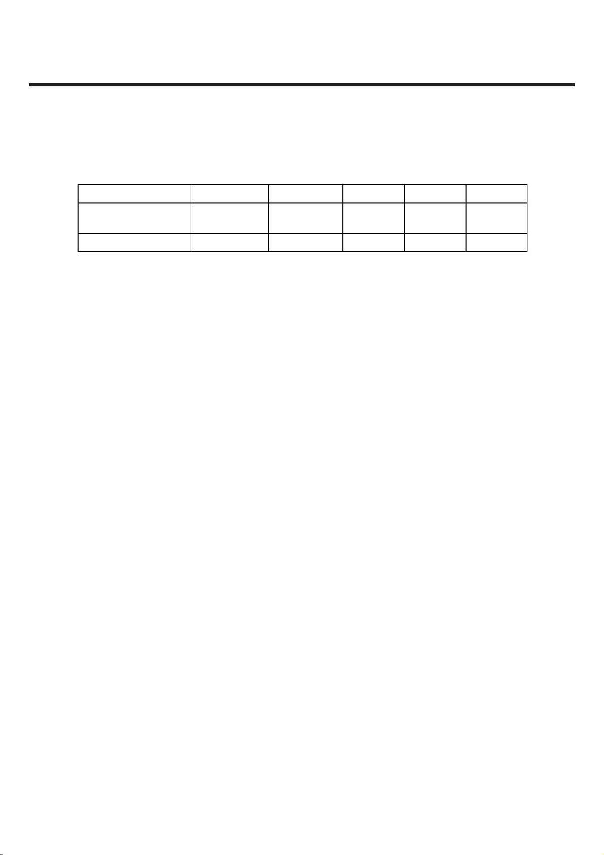
2.8 SAR characteristic
Conducted
Power [dBm]
GSM1900GSM1800GSM900WCDMA 800 WCDAM 2100Band
29.529.532.522.522.5
under 1.6 under 1.6under 1.6under 1.6under 1.6SAR(10g)[mW/g]
LGE Internal Use Only Copyright © 2009 LG Electronics. Inc. All right reserved.
- 18 -
Only for training and service purposes
3. TECHNICAL BRIEF
L-06A
L-06A
3. TECHNICAL BRIEF
3.1 General Description
The L-06A supports UMTS-800, UMTS-2100, GSM-900, DCS-1800, and PCS-1900 based GSM/GPRS/UMTS. All
receivers and the UMTS transmitter use the radioOne
frequencies, directly converting signals between RF and baseband. The tri-band GSM transmitters use a
baseband-to-IF upconversion followed by an offset phase-locked loop that translates the GMSK-modulated or
8-PSK-modulated signal to RF.
1
Zero-IF architecture to eliminate intermediate
Fig 3.1-1 Block diagram of RF part
1
QUALCOMM’s branded chipset that implements a Zero-IF radio architecture.
Copyright © 2009 LG Electronics. Inc. All right reserved.
Only for training and service purposes
- 19 -
LGE Internal Use Only

3. TECHNICAL BRIEF
L-06A
A generic, high-level functional block diagram of L-06A is shown in Figure 3-1. One antenna collects base
station forward link signals and radiates handset reverse link signals. The antenna connects with receive and
transmit paths through a FEM(Front End Module) (plus two duplexers for UMTS high-band and low-band
operations).
The UMTS receive paths each include an LNA, an RF band-pass filter, and a downconverter that translate the
signal directly from RF-to-baseband using radioOne ZIF techniques.
The high-band UMTS receive path and low-band path are accommodated in the RTR6280 IC. The RFIC.s Rx
analog baseband outputs, for the receive chains, connect to the MSM IC. The UMTS and GSM Rx baseband
outputs share the same inputs to the MSM IC .
For the transmit chains, the RTR6280 IC directly translates the Tx baseband signals (from the MSM device) to
an RF signal using an internal LO generated by integrated on-chip PLL and VCO. The RTR6280 IC outputs
deliver fairly high-level RF signals that are first filtered by Tx SAWs and then amplified by their respective
UMTS PAs. The high- and low-band UMTS RF transmit signals emerge from the RTR6280 transceiver.
In the GSM receive path, the received RF signals are applied through their band-pass filters and
down-converted directly to baseband in the RTR6280 transceiver IC. These baseband outputs are shared with
the UMTS receiver and routed to the MSM IC for further signal processing. .
The GSM transmit path employs one stage of up-conversion and, in order to improve efficiency, is divided
into phase and amplitude components to produce an open-loop Polar topology:
1. The on-chip quadrature up-converter translates the GMSK-modulated signal or 8-PSK modulated signal, to
a constant envelope phase signal at RF;
2. The amplitude-modulated (AM) component is applied to the ramping control pin of Polar
power amplifier from a DAC within the MSM
LGE Internal Use Only Copyright © 2009 LG Electronics. Inc. All right reserved.
- 20 -
Only for training and service purposes

3. TECHNICAL BRIEF
L-06A
L-06A power supply voltages are managed and regulated by the PM7540 Power Management IC. This
versatile device integrates all wireless handset power management, general housekeeping, and user interface
support functions into a single mixed signal IC. It monitors and controls the external power source and
coordinates battery recharging while maintaining the handset supply voltages using low dropout,
programmable regulators.
The device’s general housekeeping functions include an ADC and analog multiplexer circuit for monitoring
on-chip voltage sources, charging status, and current flow, as well as user-defined off-chip variables such as
temperature, RF output power, and battery ID. Various oscillator, clock, and counter circuits support IC and
higher-level handset functions. Key parameters such as under-voltage lockout and crystal oscillator signal
presence are monitored to protect against detrimental conditions.
Copyright © 2009 LG Electronics. Inc. All right reserved.
Only for training and service purposes
- 21 -
LGE Internal Use Only
3. TECHNICAL BRIEF
L-06A
3.2 GSM Mode
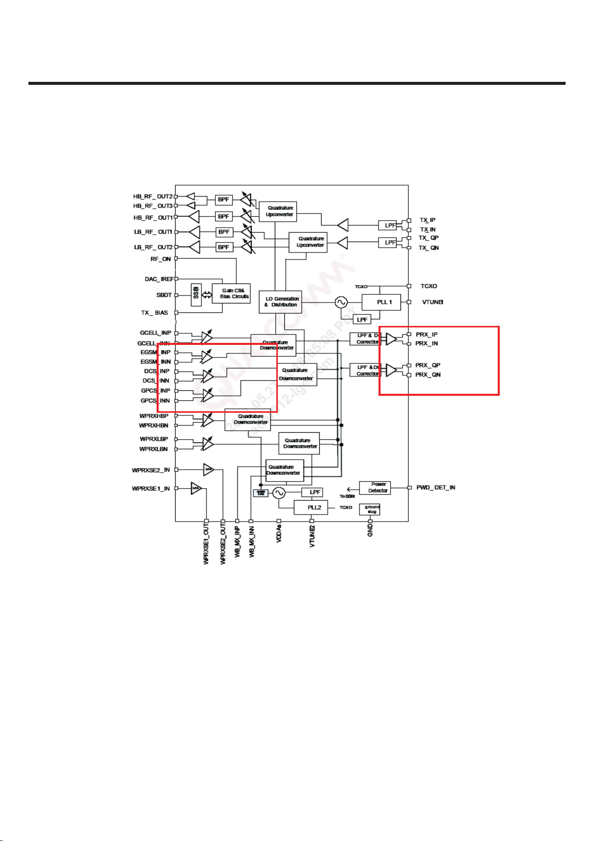
3.2.1 GSM Receiver
The Dual-mode L-06A’s receiver functions are split between the three RFICs as follows:
■ UMTS-800, UMTS-2100, GSM-900, DCS-1800, and PCS-1900 modes use the RTR6280 IC only. Each mode has
independent front-end circuits and down-converters, but they share common baseband circuits (with only
one mode active at a time). All receiver control functions are beginning with SSBI-controlled parameters.
RF Front end consists of antenna, antenna switch module(LMSP43QL-771) which includes four RX
saw filters(GSM850, GSM900, DCS and PCS). The antenna switch module allows multiple
operating bands and modes to share the same antenna.
In L-06A, a common antenna connects to one of eight paths:
1) UMTS-800 Rx/Tx, 2) UMTS-1900 Rx/Tx, 3) GSM-900 Rx, 4) GSM-900 Tx,
5) DCS-1800 Rx, 6) PCS-1900 Rx, 7) DCS-1800 TX, 8) PCS-1900 TX.
UMTS operation requires simultaneous reception and transmission, so the UMTS
Rx/Tx connection is routed to a duplexer that separates receive and transmit signals.
GSM850/GSM900, DCS, and PCS operation is time division duplexed, so only the receiver
or transmitter is active at any time and a frequency duplexer is not required.
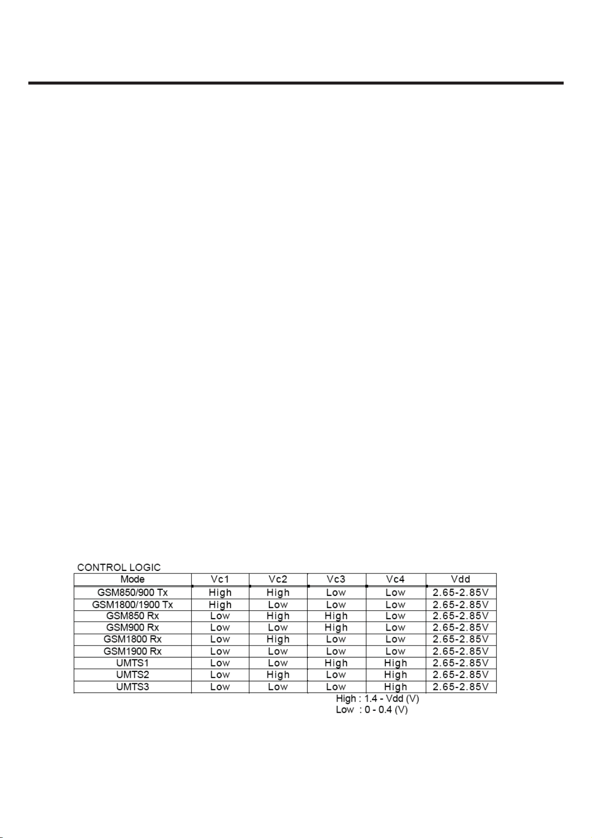
Table 3.2-1 Antenna Switch Module Control logic
LGE Internal Use Only Copyright © 2009 LG Electronics. Inc. All right reserved.
- 22 -
Only for training and service purposes

3. TECHNICAL BRIEF
L-06A
The GSM900, DCS, and PCS receiver inputs of RTR6280 are connected directly to the transceiver front-end
circuits(filters and antenna switch module). GSM900, DCS, and PCS receiver inputs use differential
configurations to improve common-mode rejection and second-order non-linearity performance. The
balance between the complementary signals is critical and must be maintained from the RF filter outputs all
the way into the IC pins. The RTR6280 input stages include MSM-controlled gain adjustments that maximize
receiver dynamic range.
Since GSM900, DCS, and PCS signals are time-division duplex (the handset can only receive or transmit at one
time), switches are used to separate Rx and Tx signals in place of frequency duplexers – this is accomplished
in the switch module.
. The amplifier outputs drive the RF ports of the quadrature RF-to-baseband downconverters. The
downconverted baseband outputs are multiplexed and routed to lowpass filters (one I and one Q) having
passband and stopband characteristics suitable for GMSK or 8-PSK processing. These filter circuits include DC
offset corrections. The filter outputs are buffered and passed on to the MSM7200A IC for further processing.
Copyright © 2009 LG Electronics. Inc. All right reserved.
Only for training and service purposes
- 23 -
LGE Internal Use Only
3. TECHNICAL BRIEF
L-06A
Fig 3.2-1 RTR6280 RX feature
LGE Internal Use Only Copyright © 2009 LG Electronics. Inc. All right reserved.
- 24 -
Only for training and service purposes
3. TECHNICAL BRIEF
L-06A
L-06A
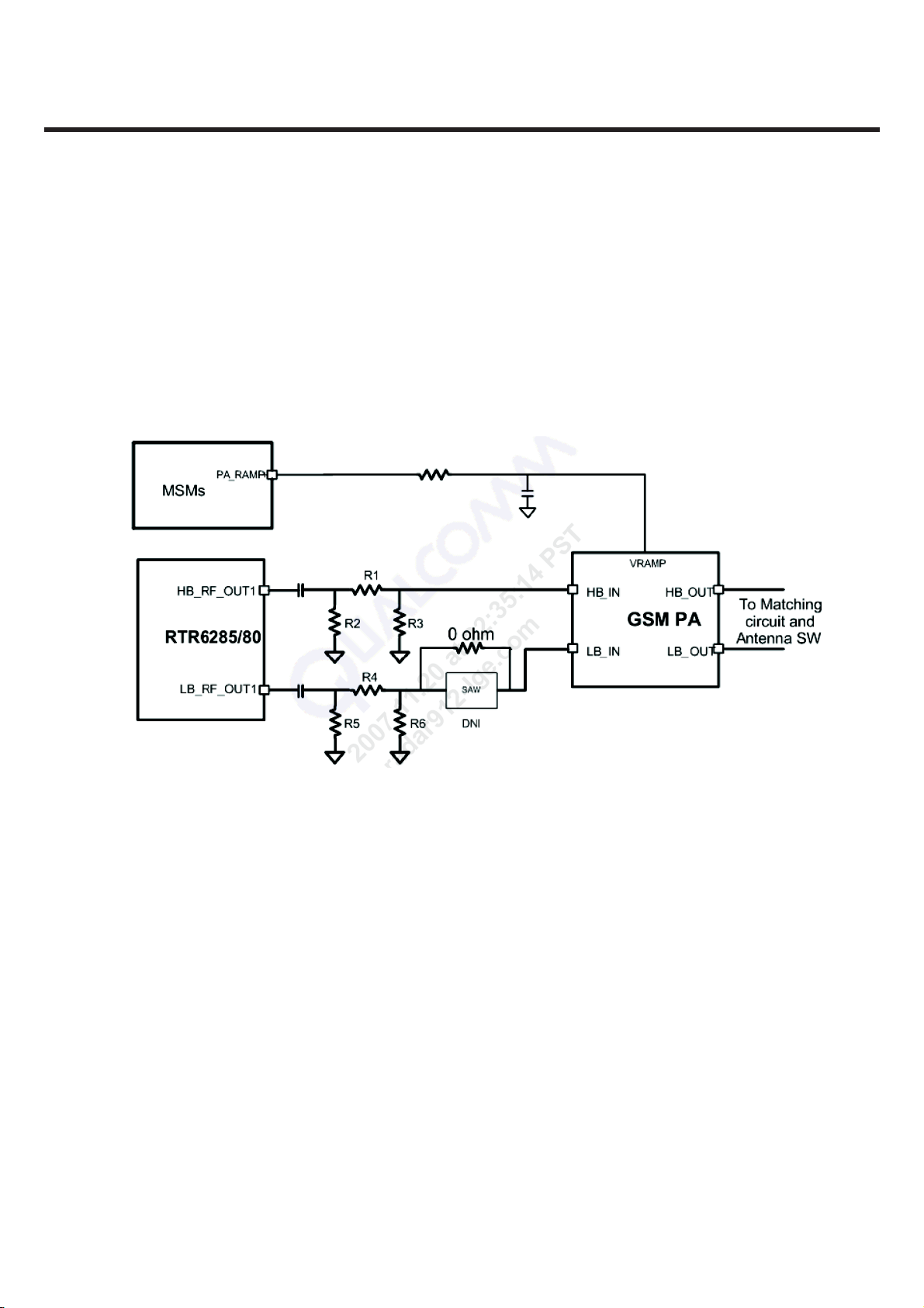
3.2.2 GSM Transmitter
The RTR6280 transmitter outputs(HB_RF_OUT1 and LB_RF_OUT1)include on-chip output matching inductors.
50ohm output impedance is achieved by adding a series capacitor at the output pins. The capacitor value
may be optimized for specific applictions and PCB characteristics based on pass-band symmetry about the
band center frequency, the suggested starting value is shown in Figure3.2.
Figure 3.2-2 GSM Transmitter matching
The RTR6280 IC is able to support GSM 850/1900 and GSM 1800/1900 mode transmitting.
This design guideline shows a quad-band GSM application.
Both high-band and low band outputs are followed by resistive pads to ensure that the load
Presented to the outputs remains close to 50ohm. The low-band GSM. Tx sSAW can be eliminated because
ETSI spec requires mid channels to pass RX Band noise only.
Copyright © 2009 LG Electronics. Inc. All right reserved.
Only for training and service purposes
- 25 -
LGE Internal Use Only

3. TECHNICAL BRIEF
L-06A
3.3 UMTS Mode
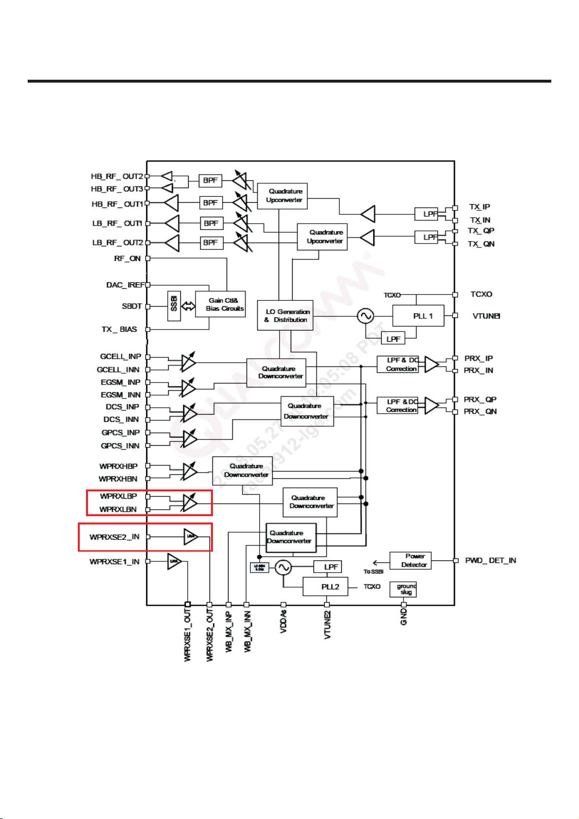
3.3.1 Receiver
The UMTS duplexer receiver outputs are routed to LNA circuits within the RTR6280 device.
The RTR6285/RTR6280 receive paths include four WCDMA Rx signal paths(two single-ended and two
differential) for one UMTS low-band and three UMTS high-bands.
LGE Internal Use Only Copyright © 2009 LG Electronics. Inc. All right reserved.
- 26 -
Only for training and service purposes
3. TECHNICAL BRIEF
L-06A
WCDMA_800_RX
WCDMA_2100_RX
Figure 3.3-1 RTR6280 IC functional block diagram
Copyright © 2009 LG Electronics. Inc. All right reserved.
Only for training and service purposes
- 27 -
LGE Internal Use Only

3. TECHNICAL BRIEF
L-06A
The two RTR6285/RTR6280 UMTS single-ended inputs accept its UMTS 2100/1900/1800/1700 input signal
from the handset RF front-end filters. The UMTS Rx inputs are provided with onchip LNAs that amplify the
signal before second-stage filters that provide differential signal to a shared downconverter. This second-
stage input is configured differentially to optimize secondorder inter-modulation and common mode
rejection performance. The gain of the UMTS front-end amplifier and the UMTS second-stage differential
amplifier are adjustable, under MSM control, to extend the dynamic range of the receivers.
The second-stage UMTS Rx amplifiers drive the RF ports of the quadrature RF-to-baseband downconverters.
The downconverted UMTS Rx baseband outputs are routed to lowpass filters having passband and stopband
characteristics suitable for UMTS Rx processing. These filter circuits allow DC-offset corrections, and their
differential outputs are buffered to interface with the MSM IC.
The RTR6285/RTR6280 UMTS differential input paths stay on-chip; off-chip inter-stage filtering is not required.
Other than this, the architecture is similar to the single-ended inputs. The UMTS duplexer receiver output is
routed to LNA circuits within the RTR6280 device. UMTS LNA circuits(one for low-band UMTS and one for
high-band UMTS path) separated from all other receive functions contained within the RTR6280 IC to improve
mixer LO to RF isolation- a critical parameter in the ZIF architecture. Isolation is further improved using high-
reverse isolation circuits in the LNA designs
LGE Internal Use Only Copyright © 2009 LG Electronics. Inc. All right reserved.
- 28 -
Only for training and service purposes

3. TECHNICAL BRIEF
L-06A
3.3.2 Transmitter
The RTR6285/RTR6280 transmit includes four transmit signal paths with five outputs (three high bands and
two low bands) supporting multi-band and multi-mode GSM/GPRS/EDGE polar transmit and WCDMA/HSDPA
transmit architectures. The transmit path begins with differential baseband signals (I and Q) from the MSM
device.
These analog input signals are buffered, filtered by low-pass filters, amplified, and then applied to the
quadrature upconverter mixers. The upconverter outputs are amplified by multiple variable gain stages that
provide transmit AGC control. SSBI control from the MSM IC is used to generate the gain range control signal.
The AGC outputs are then applied to the high-band and low-output driver amplifiers; the specified driver
amplifier output level is achieved while supporting the GSM/EDGE and UMTS transmit standard’s
requirements for GSM ORFS, carrier and image suppression, WCDMA ACLR, spurious emissions, Rx-band noise,
and so forth. Again, the upconverter LO signals are generated by circuits described in Section 1.2.3. These
upconverters translate the polar GMSK-modulated or 8-PSK modulated baseband PM signals and/or WCDMA
baseband signals directly to the RF signals, which are filtered and fed into the GSM/EDGE polar PA and/or
WCDMA PA. The WCDMA TX power is coupled back to the RTR6285/RTR6280 internal power detector input
pin, PWD_DET_IN, using a coupler for power measurement.
The low-band drive amplifiers are used to transmit the polar phase modulated (PM) signal for GSM/EDGE
850/900 while the high-band driver amplifiers are for the GSM/EDGE 1800/1900.
By using the radioOne architecture, the same high-band transmit path can be used to transmit the UMTS
2100/1900/1800/1700 signal, and the low-band transmit path can be used to transmit the UMTS 800/850/900
signal, depending on the application. The envelope path is used in polar mode of operation for GSM and
EDGE. Input from the MSM IC, the baseband envelope (AM) signal, is applied directly to the ramp control pin
of the GSM/EDGE polar PA to modulate the power supply of the PA so that the polar modulated GSM/EDGE
signal in the MSM can be recovered and transmitted.
Copyright © 2009 LG Electronics. Inc. All right reserved.
Only for training and service purposes
- 29 -
LGE Internal Use Only
3. TECHNICAL BRIEF
L-06A
WCDMA_2100_TX
WCDMA_800_TX
Fig.3.3-2 RTR6280 IC functional block diagram
LGE Internal Use Only Copyright © 2009 LG Electronics. Inc. All right reserved.
- 30 -
Only for training and service purposes
3. TECHNICAL BRIEF
L-06A
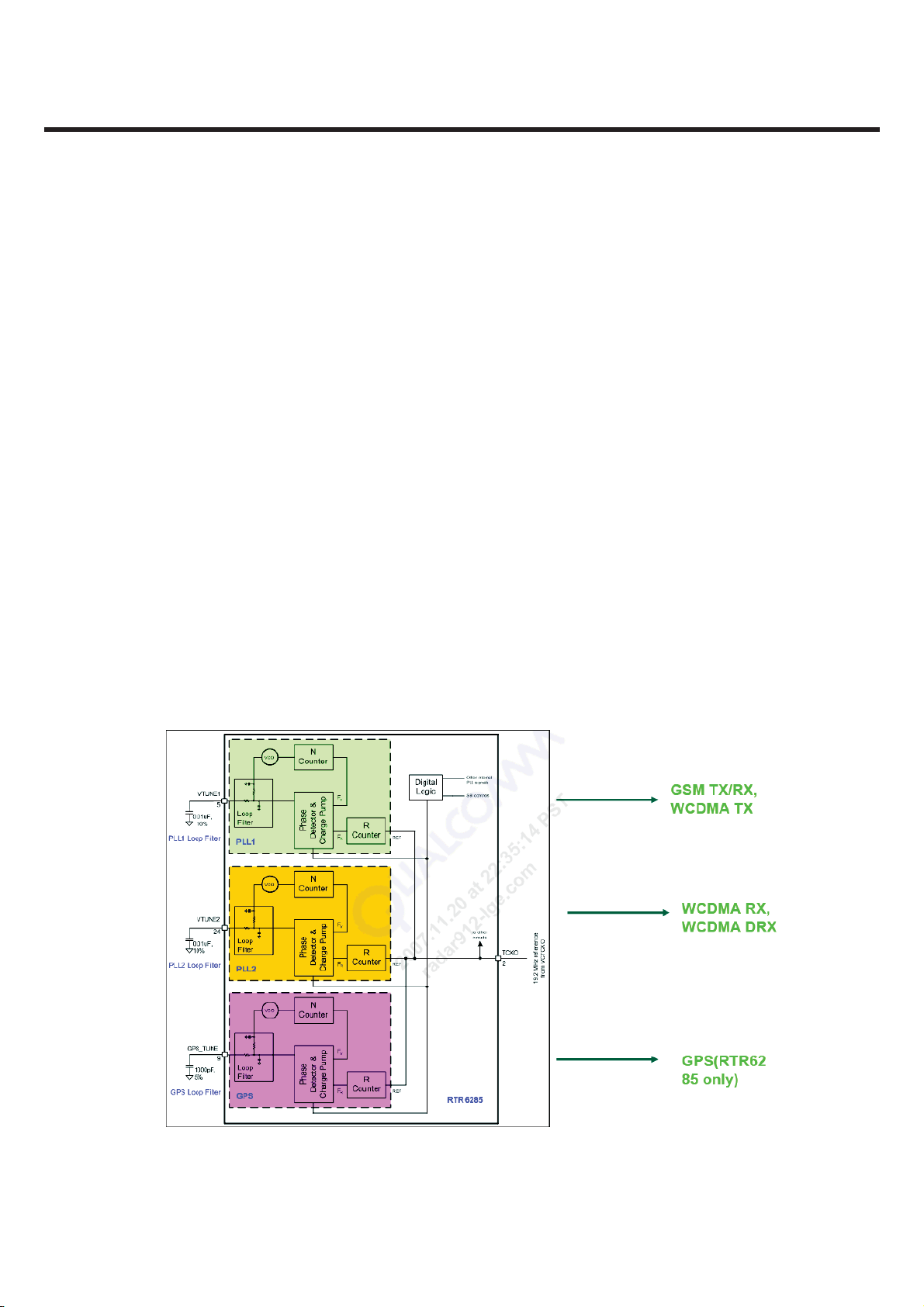
3.4 LO Phase-locked Loop
The integrated LO generation and distribution circuits are driven by internal VCOs to support various modes
to yield highly flexible quadrature LO outputs that drive all GSM/EDGE, UMTS band and GPS upconverters and
downconverters; with the help of these LO generation and distribution circuits, true zero-IF architecture is
employed in all GSM and UMTS band receivers and transmitters to translate the signal directly from RF-to-
baseband and from baseband-to-RF.
Two fully functional fractional-N synthesizers, including VCOs and loop filters, are integrated within the
RTR6285/RTR6280 IC. In addition, the RTR6285 has a third synthesizer used for GPS operation. The first
synthesizer (PLL1) in the RTR6285/6280 creates the transceiver LOs that support the UMTS transmitter, and all
four GSM band receivers and transmitters including: GSM 850, GSM 900, GSM 1800, and GSM 1900. The
second synthesizer (PLL2) in the RTR6285/RTR6280 IC provides the LO for the UMTS primary receiver. For the
RTR6285 IC only, the second synthesizer also provides the LO for the secondary UMTS receiver. The third
synthesizer (PLL3), only in the RTR6285 IC, provides the LO for the GPS receiver. An external TCXO input signal
is required to provide the synthesizer frequency reference to which the PLL is phase and frequency locked.
The RTR6285/RTR6280 ICs integrate most of the PLL loop filter components on-chip except for three off-chip
loop filter-series capacitors, which significantly reduces off-chip component requirement. With the integrated
fractional-N PLL synthesizers, the RTR6285/RTR6280 ICs have the advantage of more flexible loop bandwidth
control, fast lock time, and low-integrated phase error.
Fig.3.4-1. RTR6280 PLL’s functional block diagram
Copyright © 2009 LG Electronics. Inc. All right reserved.
Only for training and service purposes
- 31 -
LGE Internal Use Only
 Loading...