


CDMA Mobile Subscriber Unit
LG-KV800
SERVICE MANUAL
Dual BAND, Dual MODE
[GPS/CELLULAR]
CDMA MOBILE PHONE
Copyright©2009 LG Electronics. Inc. All right reserved. LGE Internal Use Only
Only for training and service purpose.
1

Table of Contents
General Introduction
CHAPTER 1. System Introduction
1.1. System Introduction……………..……..2
1.2. Features and Advantages of CDMA
Mobile Phone (For AMPS as well)..….3
1.3. Structure and Functions of dual-band
CDMA Mobile Phone……………...….6
1.4. Specification……………………………7
1.5. Installation…………………………….10
CHPATER 2. NAM Input Method
2.1. NAM Program Method and Telephone
Number Inputting Method……………11
CHAPTER 3. Circuit Description
3.1. RF Transmit/Receive Part…………….12
………...……………...1
4.2.7 Check Coupler & Duplexer &
Diplexer & Mobile S/W…...………41
4.3 Logic part Trouble
4.3.1 Power ON trouble…………………43
4.3.2 Battery Charging trouble………….46
4.3.3 Camera trouble……………………49
4.3.4 LCD trouble………………………52
4.3.5 Speaker trouble……………………55
4.3.6 MIC trouble……………………….58
4.3.7 Headset trouble……………………61
4.3.8 Keypad Backlight trouble…………66
4.3.9 Motor trouble……………………..68
4.3.10 BLUETOOTH trouble…………..71
4.3.11 Touch Sensor trouble……………74
CHAPTER 5. Safety
.....................................77
3.2. Digital/Voice Processing Part…...……17
CHAPTER 4. Trouble Shooting
4.1 Rxpart Trouble
4.1.1 When Rx Power isn't enough…......21
4.1.2 Check Regulator(PMIC) Circuit….22
4.1.3 Check TCXO circuit……………...23
4.1.4 Check Mobile S/W & Diplexer &
Duplexer………………………….24
4.1.5 Check LNA & SAW………………26
4.1.6 Check SBI control Signal………....28
4.1.7 Check Rx I/Q data………………...30
4.2 Tx part Trouble………………………..32
4.2.1 Check Regulator(PMIC) Circuit….33
4.2.2 Check TCXO Circuit……………..34
4.2.3 Check SBI Control Signal………...35
4.2.4 Check RFT6150 Circuit…………..36
CHAPTER 6. Glossary
CHAPTER 7. APPENDIX
7.1 KV800 Block and Circuit diagram…....94
7.1.1 KV800 RF Block diagram……......95
7.1.2 KV800 LOGIC Block diagram.......96
7.1.3 KV800 Main PCB Circuit….......…99
7.1.4.KV800 Sub PCB Circuit….…...104
7.1.5 KV800 RF FPCB..........................106
7.2 KV800 BGA PIN Map……………….107
7.3 KV800 Component Layout...………...112
7.4. KV800 Exploded view……….……...118
7.4.1 KV800 Assy view……….……....119
7.4.2 KV800 Full view………….……..120
7.5 KV800 Part List……………………...121
7.5.1 KV800 Main PCB Part List…..…122
…..…………………80
….……………...93
4.2.5 Check HDET Circuit……………...38
4.2.6 Check PAM Circuit……………….39
Copyright©2009 LG Electronics. Inc. All right reserved. LGE Internal Use Only
Only for training and service purpose.
1
7.5.2 KV800 Sub PCB Part List..……..131
7.5.3 KV800 RF FPCB part list……….135

General Introduction
The LG-KV800 phone has been designed to operate on the latest digital mobile communication technology,
Code Division Multiple Access (CDMA). This CDMA digital technology has greatly enhanced voice clarity and
can provide a variety of advanced features. The LG-KV800 support GPS Mode, we usually call it dual-band
phone.
The CDMA technology adopts DSSS (Direct Sequence Spread Spectrum). This feature of DSSS enables the
phone to keep communication from being crossed and to use one frequency channel by multiple users in the
same specific area, resulting that it increases the capacity 10 times more compared with that in the analog mode
currently used. Soft/Softer Handoff, Hard Handoff, and Dynamic RF power Control technologies are combined
into this phone to reduce the call being interrupted in a middle of talking over the phone. CDMA network
consists of MSO (Mobile Switching Office), BSC (Base Station Controller), BTS (Base station Transmission
System), and MS (Mobile Station). The following table lists some major CDMA Standards.
CDMA Standard Designator Description
Basic air interface TIA/EIA/IS-95-A/B/C
ANSI J-STD-008
Network TIA/EIA/IS-634
TIA/EIA/IS/651
TIA/EIA/IS-41-C
TIA/EIA/IS-124
Service TIA/EIA/IS-96-B
TIA/EIA/IS-99
TIA/EIA/IS-637
TIA/EIA/IS-657
Performance TIA/EIA/IS-97
TIA/EIA/IS-98
ANSI J-STD-018
ANSI J-STD-019
TIA/EIA/IS-125
* TSB –74: Protocol between an IS-95A system and ANSI J-STD-008
Protocol between MS and BTS for Cellular & AMPS
Protocol between MS and BTS for PCS
MAS-BS
PCSC-RS
Intersystem operations
Nom-signaling data comm.
Speech CODEC
Assign data and fax
Short message service
Packet data
Cellular base station
Cellular mobile station
PCS personal station
PCS base station
Speech CODEC
Copyright©2009 LG Electronics. Inc. All right reserved. LGE Internal Use Only
Only for training and service purpose.
1

Chapter 1. System Introduction
1. System Introduction
1.1 CDMA Abstract
The CDMA mobile communication system has a channel hand-off function that is used for collecting the
information on the locations and movements of mobile telephones from the cell site by automatically controlling
several cell site through the setup of data transmission routes, and then enabling one switching system to carry
out the automatic remote adjustment. This is to maintain continuously the call state through the automatic
location confirmation and automatic radio channel conversion when the busy subscriber moves from the service
area of one cell site to that of another by using automatic location confirmation and automatic radio channel
conversion functions. The call state can be maintained continuously by the information exchange between
switching systems when the busy subscriber moves from one cellular system area to the other cellular system
area.
In the cellular system, the cell site is a small-sized low output type and utilizes a frequency allocation system
that considers mutual interference, in an effort to enable the re-use of corresponding frequency from a cell site
separated more than a certain distance. The analog cellular systems are classified further into an AMPS system,
E-AMPS System, NMT system, ETACS system, and JTACS system depending on technologies used.
Unlike the time division multiple access (TDMA) or frequency division multiple access (FDMA) used in the
band limited environment, the Code Division Multiple Access (CDMA) system which is one of digital cellular
systems is a multi-access technology under the interference limited environment. It can process more number of
subscribers compared to other systems (TDMA system has the processing capacity three times greater than the
existing FDMA system whereas CDMA system, about 12~15 times of that of the existing system).
CDMA system can be explained as follows; TDMA or CDMA can be used to enable each person to talk
alternately or provide a separate room for each person when two persons desire to talk with each other at the
same time, whereas FDMA can be used to enable one person to talk in soprano, whereas the other in bass (one
of the two talkers can carry out synchronization for hearing in case there is a bandpass filter function in the area
of the hearer). Another available method is to make two persons to sing in different languages at the same time,
space, and frequency when wishing to let the audience hear the singing without being confused. This is the
characteristic of CDMA.
On the other hand, when employing the CDMA technology, each signal has a different pseudo-random binary
sequence used to spread the spectrum of carrier. A great number of CDMA signals share the same frequency
spectrum. In the perspective of frequency area or time area, several CDMA signals are overlapped. Among these
types of signals, only desired signal energy is selected and received through the use of pre-determined binary
sequence; desired signals can be separated, and then received with the correlator used for recovering the
spectrum into its original state. At this time, the spectrums of other signals that have different codes are not
recovered into its original state, and appears as the self-interference of the system.
Copyright©2009 LG Electronics. Inc. All right reserved. LGE Internal Use Only
Only for training and service purpose.
2

1.2. Features and Advantages of CDMA Mobile Phone
1.2.1 Various Types of Diversities
When employing the narrow band modulation (30kHz band) that is the same as the analog FM modulation
system used in the existing cellular system, the multi-paths of radio waves create a serious fading. However, in
the CDMA broadband modulation (1.25MHz band), three types of diversities (time, frequency, and space) are
used to reduce serious fading problems generated from radio channels in order to obtain high-quality calls.
Time diversity can be obtained through the use of code interleaving and error correction code whereas frequency
diversity can be obtained by spreading signal energy to wider frequency band. The fading related to normal
frequency can affect the normal 200~300kHz among signal bands and accordingly, serious effect can be avoided.
Moreover, space diversity (also called path diversity) can be realized with the following three types of methods.
First, it can be obtained by the duplication of cell site receive antenna. Second, it can be obtained through the
use of multi-signal processing device that receives a transmit signal having each different transmission delay
time and then, combines them. Third, it can be obtained through the multiple cell site connection (Soft Handoff)
that connects the mobile station with more than two cell sites at the same time.
1.2.2 Power Control
The CDMA system utilizes the forward (from a base station to mobile stations) and backward (from the mobile
station to the base station) power control in order to increase the call processing capacity and obtain high-quality
calls. In case the originating signals of mobile stations are received by the cell site in the minimum call quality
level (signal to interference) through the use of transmit power control on all the mobile stations, the system
capacity can be maximized. If the signal power of mobile station is received too strong, the performance of that
mobile station is improved. However, because of this, the interference on other mobile stations using the same
channel is increased and accordingly, the call quality of other subscribers is reduced unless the maximum
accommodation capacity is reduced.
In the CDMA system, forward power control, backward open loop power control, and closed loop power control
methods are used. The forward power control is carried out in the cell site to reduce the transmit power on
mobile stations less affected by the multi-path fading and shadow phenomenon and the interference of other cell
sites when the mobile station is not engaged in the call or is relatively nearer to the corresponding cell site. This
is also used to provide additional power to mobile stations having high call error rates, located in bad reception
areas or far away from the cell site.
The backward open loop power control is carried out in a corresponding mobile station; the mobile station
measures power received from the cell site and then, reversely increases/decreases transmit power in order to
compensate channel changes caused by the forward link path loss and terrain characteristics in relation to the
mobile station in the cell site. By doing so, all the mobile transmit signals received by the base station have same
strength.
Moreover, the backward closed loop power control used by the mobile station is performed to control power
using the commands issued out by the cell site. The cell site receives the signal of each corresponding mobile
station and compares this with the pre-set threshold value and then, issues out power increase/decrease
commands to the corresponding mobile station every 1.25msec (800 times per second). By doing so, the gain
tolerance and the different radio propagation loss on the forward/backward link are complemented.
Copyright©2009 LG Electronics. Inc. All right reserved. LGE Internal Use Only
Only for training and service purpose.
3

1.2.3 Voice Encoder and Variable Data Speed
The bi-directional voice service having variable data speed provides voice communication which employs
voice encoder algorithm having power variable data rate between the base station and the mobile station. On the
other hand, the transmit voice encoder performs voice sampling and then, creates encoded voice packets to be
sent out to the receive voice encoder, whereas the receive voice encoder demodulates the received voice packets
into voice samples.
One of the two voice encoders described in the above is selected for use depending on inputted automatic
conditions and message/data; both of them utilize four-stage frames of 9600, 4800, 2400, and 1200 bits per
second for cellular. In addition, this type of variable voice encoder utilizes adaptive threshold values on
selecting required data rate. It is adjusted in accordance with the size of background noise and the data rate is
increased to high rate only when the voice of caller is inputted.
Therefore, background noise is suppressed and high-quality voice transmission is possible under the
environment experiencing serious noise. In addition, in case the caller does not talk, data transmission rate is
reduced so that the transmission is carried out in low energy. This will reduce the interference on other CDMA
signals and as a result, improve system performance (capacity increased by about two times).
1.2.4 Protecting Call Confidentiality
Voice privercy is provided in the CDMA system by means of the private long code mask used for PN spreading.
Voice privacy can ve applied on the traffic channels only. All calls are initiated using the public long code mask
for PN spreading. The mobile station user may request voice privacy during call setup using the origination
message or page response message, and during traffic channel operation using the long code transition request
order.
The Transition to private long code mask will not be performed if authentication is not performed. To initiate a
transition to the private or public long code mask, either the base station or the mobile station sends a long code
transition request order on the traffic channel.
1.2.5 Soft Handoff
A handoff in which the mobile station commences communications with a new base station without interrupting
communications with the old base station. Soft handoff can only be used between CDMA channels having
identical freqeuncy assignments.
1.2.6 Frequency Re-Use and Sector Segmentation
Unlike the existing analog cellular system, the CDMA system can reuse the same frequency at the adjacent cell.
there is no need to prepare a separate frequency plan. Total interference generated on mobile station signals
received from the cell site is the sum of interference generated from other mobile stations in the same cell site
and interference generated from the mobile station of adjacent cell site. That is, each mobile station signal
Copyright©2009 LG Electronics. Inc. All right reserved. LGE Internal Use Only
Only for training and service purpose.
4

generates interference in relation to the signals of all the other mobile stations.
Total interference from all the adjacent cell sites is the ratio of interference from all the cell sites versus total
interference from other mobile stations in the same cell site (about 65%). In the case of directional cell site, one
cell normally uses a 120°sector antenna in order to divide the sector into three. In this case, each antenna is used
only for 1/3 of mobile stations in the cell site and accordingly, interference is reduced by 1/3 on the average and
the capacity that can be supported by the entire system is increased by three times.
1.2.7 Soft Capacity
The subscriber capacity of the CDMA system is flexible depending on the relation between the number of
users and service classes. For example, the system operator can increase the number of channels available for
use during the busy hour despite the drop in call quality. This type of function requires 40% of normal call
channels in the standby mode during the handoff, in an effort to avoid call disconnection resulting from the lack
of channels.
In addition, in the CDMA system, services and service charges are classified further into different classes so that
more transmit power can be allocated to high class service users for easier call set-up; they can also be given
higher priority of using hand-off function than the general users.
Copyright©2009 LG Electronics. Inc. All right reserved. LGE Internal Use Only
Only for training and service purpose.
5

1.3. Structure and Functions of tri-band CDMA Mobile Phone
The hardware structure of CDMA mobile phone is made up of radio frequency (RF) part and logic part. The
RF part is composed of Receiver part (Rx), Transmitter part (Tx) and Local part (LO). For the purpose of
operating on tri-band, It is necessary dual Tx path, tri Rx path, dual PLL and switching system for band
selection. The mobile phone antenna is connected with the diplexer which divide antenna input/output cellular
frequency band (824~894 Mhz) and GPS frequency band(1575.42 MHz). The cellular path is linked with the
cellular duplexer. Duplexer carrys out seperating Rx band and Tx band. The Rx signals from the antenna are
converted into intermediate frequency(IF) band by the frequency synthesizer and frequency down converter.
And then, pass SAW filter which is a band pass filter for removing out image frequency. The IF output signals
that have been filtered is converted into digital signals via Analog-to-Digital Converter (ADC). In front of the
ADC, switching system is required to choose which band path should be open.
The digital signals send to 5 correlators in each CDMA de-modulator. Of these, one is called a searcher whereas
the remaining 4 are called data receivers (fingers). Digitalized IF signals include a great number of call signals
that have been sent out by the adjacent cells. These signals are detected with pseudo-noise sequence (PN
equence).
Signal to interference ratio (C/I) on signals that match the desired PN sequence are increased through this type
of correlation detection process, but other signals obtain processing gain by not increasing the ratio. The carrier
wave of pilot channel from the cell site most adjacently located is demodulated in order to obtain the sequence
of encoded data symbols. During the operation with one cell site, the searcher searches out multi-paths in
accordance with terrain and building reflections. On three data receivers, the most powerful 3 paths are allocated
for the parallel tracing and receiving. Fading resistance can be improved a great deal by obtaining the diversity
combined output for de-modulation. Moreover, the searcher can be used to determine the mostpowerful path
from the cell sites even during the soft handoff between the two cell sites. Moreover, 3 data receivers are
allocated in order to carry out the de-modulation of these paths. Output data that has been demodulated changes
the data string in the combined data row as in the case of original signals(deinterleaving), and then, are
demodulated by the forward error correction decoder which uses the Viterbi algorithm. Mobile station user
information send out from the mobile station to the cell site pass through the digital voice encoder via a mike.
Then, they are encoded and forward errors are corrected through the use of convolution encoder. Then, the order
of code rows is changed in accordance with a certain regulation in order to remove any errors in the interleaver.
Symbols made through the above process are spread after being loaded onto PN carrier waves. At this time, PN
sequence is selected by each address designated in each call.
Signals that have been code spread as above are digital modulated (QPSK) and then, power controlled at the
automatic gain control amplifier (AGC Amp). Then, they are converted into RF band by the frequency
synthesizer synchronizing these signals to proper output frequencies.
Transmit signals obtained pass through the duplexer filter and then, are sent out to the cell site via the antenna.
Copyright©2009 LG Electronics. Inc. All right reserved. LGE Internal Use Only
Only for training and service purpose.
6

1.4. Specification
1.4.1 General Specification
1.4.1.1 Transmit/Receive Frequency Interval :
1) CELLULAR : 45 MHz
1.4.1.2 Number of Channels (Channel Bandwidth)
1) CELLULAR : 20 Channels
1.4.1.3 Operating Voltage : DC 3.3~4.2V
1.4.1.4 Battery Power Consumption : DC 3.7V
SLEEP IDLE MAX POWER
CELLULAR
1.4.1.5 Operating Temperature : -20°C ~ +60°C
2.5 mA 200mA 900 mA (24.2 dBm)
1.4.1.6 Frequency Stability
1) CDMA : ±0.5PPM
1.4.1.7 Antenna : Internal Antenna, 50 Ω
1.4.1.8 Size and Weight
1) Size : 104.0 (H) x 54.4 (W) x 12.85(D) mm (with 900mAh)
2) Weight : 100g (with 900mAh Battery)
1.4.1.9 Channel Spacing
1) CELLULAR : 1.25MHz
1.4.1.10 Battery Type, Capacity and Orerating Time.
Unit = Hours, Minutes
Standard (900mAh)
Standby Time DCN (Slot Cycle 2)
Talk Time DCN (Slot Cycle 2)
Copyright©2009 LG Electronics. Inc. All right reserved. LGE Internal Use Only
Only for training and service purpose.
150Min.(typical duplexer,10dBm output)
7
About 150 Hrs (SCI=2)

1.4.2 Receive Specification
1.4.2.1 Frequency Range
1) CELLULAR : 869.820 MHz ~ 893.190 MHz
2) GPS : 1575.42 MHz
1.4.2.2 Local Oscillating Frequency Range :
1) CELLULAR : 1738.08MHz ~ 1787.94MHz
2) GPS : 3150.84MHz
1.4.2.3 Sensitivity
1) CELLULAR : -104dBm (C/N 12dB or more)
2) GPS : -148.5dBm
1.4.2.4 Selectivity
1) CELLULAR : 3dB C/N Degration (With Fch±1.25 kHz : -30dBm)
1.4.2.5 Interference Rejection
1) Single Tone : -30dBm at 900 kHz (CELLULAR)
2) Two Tone : -43dBm at 900 kHz & 1700kHz(CELLULAR)
1.4.2.6 Spurious Wave Suppression : Maximum of -80dB
1.4.2.7 CDMA Input Signal Range
z Dynamic area of more than -104~ -25 dB: 79dB at the 1.23MHz band.
1.4.3 Transmit Specification
1.4.3.1 Frequency Range
1) CELLULAR : 824.820MHz ~ 848.190MHz
1.4.3.2 Output Power
1) CELLULAR : 0.236W
1.4.3.3 CDMA TX Frequency Deviation :
1) CELLULAR: +300Hz or less
1.4.3.4 CDMA TX Conducted Spurious Emissions
1) CELLULAR : 900kHz : - 42 dBc/30kHz below
1.98MHz : - 54 dBc/30kHz below
Copyright©2009 LG Electronics. Inc. All right reserved. LGE Internal Use Only
Only for training and service purpose.
8

1.4.3.5 CDMA Minimum TX Power Control
1) CELLULAR : - 50dBm below
4.4
1.
MS (Mobile Station) Transmitter Frequency
1.
4.4.1 CELLULAR mode
Ch # Center Freq. (MHz) Ch # Center Freq. (MHz)
1011
29
70
111
152
193
234
275
316
363
824.640
825.870
827.100
828.330
829.560
830.790
832.020
833.250
834.480
835.890
1.4.5 MS (Mobile Station) Receiver Frequency
1.
4.5.1 CELLULAR mode
Ch. # Center Freq. (MHz) Ch. # Center Freq. (MHz)
1011
869.640
404
445
486
527
568
609
650
697
738
779
404
837.120
838.350
839.580
840.810
842.040
843.270
844.500
845.910
847.140
848.370
882.120
29
70
111
152
193
234
275
316
363
1.
4.5.2 GPS mode : 1575.42MHz
1.
4.6 AC Adapter : See Appendix
Copyright©2009 LG Electronics. Inc. All right reserved. LGE Internal Use Only
Only for training and service purpose.
870.870
872.100
873.330
874.560
875.790
877.020
878.250
879.480
880.890
445
486
527
568
609
650
697
738
779
9
883.350
884.580
885.810
887.040
888.270
889.500
890.910
892.140
893.370

1.5. Installation
1.5.1 Installing a Battery Pack
1) The Battery pack is keyed so it can only fit one way. Align the groove in the battery pack with the rail on the
back of the phone until the battery pack rests flush with the back of the phone.
2) Slide the battery pack forward until you hear a “click”, which locks the battery in place.
1.5.2 For Adapter Use
1) Plug the adapter into a wall outlet. The adapter can be operated from a 110V source. When AC power is
connected to the adapter.
2) Insert the adapter jack into the phone with the installed battery pack.
Red light indicates battery is being charged.. Green light indicates battry is fully charged.
Copyright©2009 LG Electronics. Inc. All right reserved. LGE Internal Use Only
Only for training and service purpose.
10

CHAPTER 2. NAM Input Method
(Inputting of telephone numbers included)
2.1 NAM Programming Method and Telephone Number Input Method
Æ Enter the menu
Æ Press and hold CLR key (center key) for a few seconds and press 159753
Æ You can see following Menu
1 : Service settings
2 : Test Screen
3 : Test Call
4 : Error Screen
5 : Error Delete
6 : Select Vocoder
7 : Test Mode Settings
8 : MRU Settings
9 : A-Key Settings
10 : ADM Verufy
11 : WAP Service Settings
12 : BREW Settings
13 : Data SPD Srttings
14 : MMS Settings
15 : LCD Always On
16 : Exception ReportSys
17 : BIN CRC CHECK
Æ Press 1 : Service Mode to program MIN and NAM
Æ Press a number what you want to edit
Æ Press [edit] to edit, after input, press [OK] to save
Æ To reset the handset, press [END]
Copyright©2009 LG Electronics. Inc. All right reserved. LGE Internal Use Only
Only for training and service purpose.
11
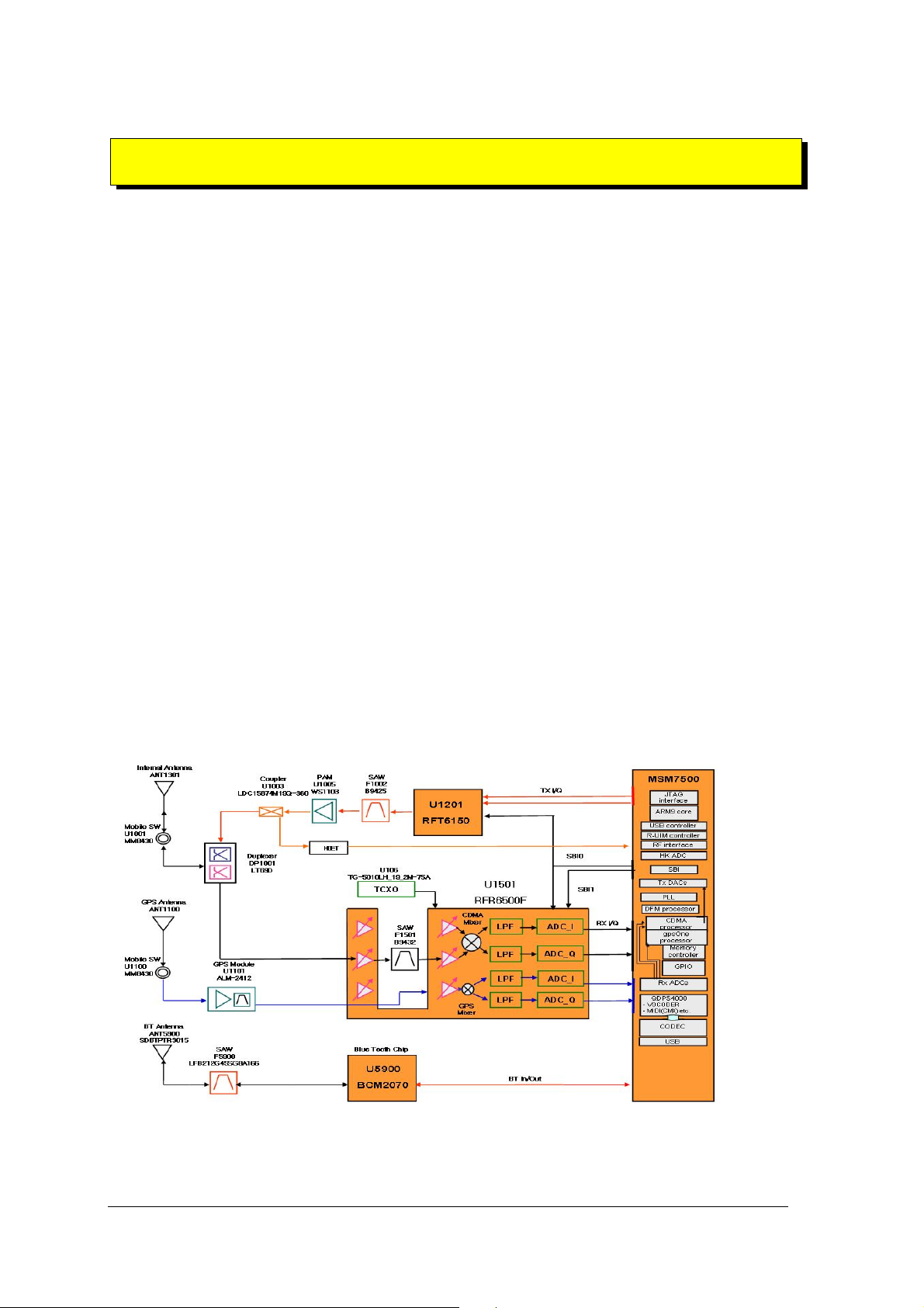
CHAPTER 3. Circuit Description
3.1. RF Transmit/Receive Part
3.1.1 Overview
The Tx and Rx part employs the Direct Conversion system. The Tx and Rx frequencies are respectively
824.04~848.97 and 869.04~893.97 for cellular. The block diagram is shown in [Figure 1-1]. RF signals received
through the antenna are seperated by one Diplexer and one Duplexer..
RF Signal fed into the low noise amplifier (LNA) which is embedded in RFR6500 through the duplexer. Then,
they are into baseband signal directly. Then, this signal is changed into digital signal by the analog to digital
converter (ADC, A/D Converter), and the digital circuit part of the MSM(Mobile Station Modem)6800A
processes the data from ADC. The digital processing part is a demodulator.
In the case of transmission, RFT6150 receives OQPSK-modulated anlog signal from the MSM7500-1. The
RFT6150 connects directly with MSM7500-1 using an analog baseband interface. In RFT6150, the baseband
quadrature signals are upconverted to the Cellular bands and amplified to provide signal drive capability to the
power amp.
After that, the RF signal is amplified by the Power Amp in order to have enough power for radiation. Finally,
the RF signal is sent out to the cell site via the antenna after going through the isolator and duplexer.
[Figure 1-1] RF Block Diagram Of KV800
Copyright©2009 LG Electronics. Inc. All right reserved. LGE Internal Use Only
Only for training and service purpose.
12
3.1.2 Description of Rx Part Circuit
3.1.2.1 Duplexer(DP1001)
The Duplexer consists of the Rx bandpass filter (BPF) and the Tx BPF which has the function of separating Tx
and Rx signals in the full duplex system for using the common antenna. The Tx part BPF is used to suppress
noises and spurious out of the Tx frequency band. The Rx BPF is used to receive only Rx signal coming from
the antenna, which is usually called preselector. It’s main function is to limit the bandwidth of spectrum
reaching the LNA and mixer, attenuate receiver spurious response and suppress local oscillator energy. As a
result frequency sensitivity and selectivity of mobile phone increase. The specification of LG-KV800 duplexer
is described below ;
● Cellular Duplexer
Pass Band
Insertion Loss
Return Loss
Attenuation
48dB min (869~894MHz) 60dB min (824~849MHz) 60dB (824~849MHz)
Tx Rx Tx to Rx (min)
824~849MHz 869~894 MHz
2.0dB max 2.5dB max
12dB min 12dB min
50dB (869~894MHz)
3.1.2.3 LNAs (U1501)
The RFR6500 has cellular LNAs, respectively. The characteristics of Low Noise Amplifier (LNA) are low
noise figure, high gain, high intercept point and high reverse isolation. The frequency selectivity characteristic
of mobile phone is mostly determined by LNA.
The specification of KV800 LNAs are described below.
● Cellular
High current mode Low current mode Passive status
Power Gain
*Gain mode G0(G2)
*Gain mode G1(G3)
Noise Figure
Gain mode G0(G2)
Gain mode G1(G3)
Input IP3
Gain mode G0(G2)
Copyright©2009 LG Electronics. Inc. All right reserved. LGE Internal Use Only
Only for training and service purpose.
16dB
4.0dB
1.4dB
4.0dB
8dB
13
14dB
3.0dB
1.4dB
4.0dB
-5dB
-6.0dB
-20.0dB
7.0dB
20.0dB
12dB

Gain mode G1(G3) 5dB -5dB 10dB
*Gain mode G0 and G1 operate in high and low current mode.
*Gain mode G2 and G3 operate in Passive status.
● GPS
Parameter GPS Band Unit
Gain 14.5 dB
Noise Figure 1.3 dB
IIP3 5.0 dBm
3.1.2.4 Down-converter Mixers
The RFR6500 device performs signal down-conversion for Cellular, PCS and GPS tri-band applications, but
LG-KV800 uses only Cellular and GPS. It contains all the circuitry (with the exception of external filters) needed
to support conversion of received RF signals to baseband signals. It consists of the three downconverting Mixers
(Cellular and GPS), and an RX VCO and RX PLL circuit.
The GPS LNA & mixers offer the most advanced and integrated CDMA Rx solution designed to meet
cascaded Noise Figure (NF) and Third-order Intercept Point (IIP3) requirements of IS-98C specifications for
Sensitivity, Two-Tone Intermodulation, and Single-tone Desense.
Operation modes and band selection are specially controlled from the Mobile Station Modem MSM7500-1.
The specification of LG-KV800 Mixers are described below:
● Cellular
High current mode Mid current mode Low current mode
Noise Figure
High Gain mode
Low Gain mode
Input IP3
High Gain mode
Low Gain mode
Input IP2
High Gain mode
10dB
25dB
4.0dB
-5.0dB
56dB
10dB
25dB
4.0dB
-5.0dB
56dB
9dB
25dB
-10.0dB
-5.0dB
40dB
Low Gain mode
30dB
30dB
30dB
Copyright©2009 LG Electronics. Inc. All right reserved. LGE Internal Use Only
Only for training and service purpose.
14

● Cellular
High current mode Mid current mode Low current mode
Noise Figure
High Gain mode
Low Gain mode
Input IP3
High Gain mode
Low Gain mode
Input IP2
High Gain mode
Low Gain mode
10dB
25dB
4.0dB
-11.0dB
56dB
30dB
10dB
25dB
-8.0dB
-11.0dB
56dB
30dB
9dB
25dB
-8.0dB
-11.0dB
40dB
30dB
3.1.2.4 Rx RF SAW FILTER(F1501)
The main function of Rx RF SAW filter is to attenuate mobile phone spurious frequency, attenuate direct RF
frequency pick up, attenuate noise at the image frequency originating in or amplified by the LNA and suppress
second harmonic originating in the LNA. The Rx RF SAW filter usually called image filter.
3.1.3 Description of Transmit Part Circuit
3.1.3.1 RFT6150 (U1201)
The RFT6150 base-band-to-RF Transmit Processor performs all Tx signal-processing functions required
between digital base-band and the Power Amplifier Modulator (PAM). The base-band quadrature signals are
up-converted to the Cellular frequency bands and amplified to provide signal drive capability to the PAM.
The RFT6150 includes an RF mixer for upconverting analog baseband to RF, a programmable PLL for
generating Tx LO frequency, two cellular driver amplifiers and Tx power control through an 85dB VGA. As
added benefit, the single sideband upconversion eliminates the need for a band pass filter normally required
between the upconverter and driver amplifier.
I, I/, Q and Q/ signals proceed from the MSM7500-1 to RFT6150 are analog signal. In CDMA mode, These
signals are modulated by Quadrature Phase Shift King (QPSK). I and Q are 90 deg. out of phase, and I and I/ are
180 deg. The mixer in RFT6150 converts baseband signals into RF signals. After passing through the
upconverter , RF signal is inputted into the Power AMP.
Copyright©2009 LG Electronics. Inc. All right reserved. LGE Internal Use Only
Only for training and service purpose.
15

● RFT6150 Cellular CDMA RF Specifications
Condition Min. Typ. Max. Units
Rated Output Power
Min Output Power
Rx band noise power
ACPR
Average CDMA Cellular
Average CDMA Cellular
CDMA Cellular
Cellular: Fc±885kHz
7 dBm
-75
-75
-136 dBm/Hz
-56 dBc/
dBm
3.1.3.2 Power Amplifier(U1005)
The power amplifier that can be used in the CDMA mode has linear amplification capability and high efficiency.
For higher efficiency, it is made up of one MMIC (Monolithic Microwave Integrated Circuit) for which RF
input terminal and internal interface circuit are integrated onto one IC after going through the AlGaAs/GaAs
HBT (heterojunction bipolar transistor) process. The module of power amplifier is made up of an output end
interface circuit including this MMIC. The maximum power that can be inputted through the input terminal is
+10dBm and conversion gain is about 28dB. RF transmit signals that have been amplified through the power
amplifier are sent to the duplexer.
3.1.4 Description of Frequency Synthesizer Circuit
3.1.4.1 Voltage Control Temperature Compensation Crystal Oscillator (VCTCXO, U106)
The temperature variation of mobile phone can be compensated by VCTCXO. The reference frequency of a
mobile phone is 19.2MHz. The receives frequency tuning signals called TRK_LO_ADJ from MSM as
0.5V~2.5V DC via R and C filter in order to generate the reference frequency of 19.2MHz and input it into the
frequency synthesizer. Frequency stability depending on temperature is ±2.0 ppm.
Copyright©2009 LG Electronics. Inc. All right reserved. LGE Internal Use Only
Only for training and service purpose.
16

3.2. Digital/Voice Processing Part
3.2.1 Overview
The digital/voice processing part processes the user's commands and processes all the digital and voice signal
processing in order to operate in the phone. The digital/voice processing part is made up of a keypad/LCD,
receptacle part, voice processing part, mobile station modem part, memory part, and power supply part.
3.2.2 Configuration
3.2.2.1 Touch pannel and Receptacle Part
This is used to transmit Touch signals to MSM7500-1 via touch control IC .
and a receptacle that receives and sends out voice and data with external sources.
3.2.2.2 Voice Processing Part
The voice processing part is made up of an audio codec used to convert MIC signals into digital voice signals
and digital voice signals into analog voice signals, amplifying part for amplifying the voice signals and sending
them to the ear piece, amplifying part that amplifies ringer signals coming out from MSM7500-1, and
amplifying part that amplifies signals coming out from MIC and transferring them to the audio processor.
3.2.2.3 MSM (Mobile Station Modem) 7500-1 Part
MSM is the core elements of CDMA terminal and carries out the functions of CPU, encoder, interleaver,
deinterleaver, Viterbi decoder, Mod/Demod, and vocoder.
3.2.2.4 Memory Part
The memory part is made up of a sdram/nand memory, nand for storing data.
3.2.2.5 Power Supply Part
The power supply part is made up of circuits for generating various types of power, used for the digital/voice
processing part.
Copyright©2009 LG Electronics. Inc. All right reserved. LGE Internal Use Only
Only for training and service purpose.
17

3.2.3 Circuit Description
3.2.3.1 Touch pannel /LCD and Receptacle Part
Once the
processing.
The terminal status and operation are displayed on the screen for the user with the characters and icons.
Moreover, it exchanges audio signals and data with external sources through the receptacle, and then receives
power from the battery or external batteries.
Touch pannel
is pressed, the touch signals are sent out to MSM7500-1 via touch control IC for
3.2.3.2 Audio Processing Part
MIC signals are amplified through OP AMP, inputted into the audio codec(included in MSM6 and converted
into digital signals. Oppositely, digital audio signals are converted into analog signals after going through the
audio codec. These signals are amplified at the audio amplifier and transmitted to the ear-piece. The signals from
MSM7500-1 activate the ringer by using signals generated in the timer in MSM7500-1.
3.2.3.3 MSM Part
The MSM7501A device integrates the ARM1136-J™ and ARM926EJ-S™ processor cores, offering the
ARM® Jazelle™ Java® hardware accelerator: one low-power, high-performance QDSP5000™ application
digital signal processor (aDSP) and one QDSP4000™ modem digital signal processor (mDSP) core, hardware
acceleration for
video, imaging, and graphics, and a wideband stereo codec to support enhanced digital audio applications. The
hardware acceleration eliminates the need for the multimedia companion processors normally required for video
and audio-based applications that support MP3 music files, a MIDI synthesizer, video and still image record and
playback,
and 2D/3D graphics functions. By removing the need for costly applications coprocessors and memory
subsystems, the MSM7501A solution reduces BOM costs and increases standby and talk times. QUALCOMM
provides a complete software suite and advance mobile subscriber software (AMSS) for building handsets based
on the MSM7501A chipset. AMSS software is designed to run on a SURF phone platform, an optional
development platform optimized to assist in evaluating, testing, and debugging AMSS software.
.
Copyright©2009 LG Electronics. Inc. All right reserved. LGE Internal Use Only
Only for training and service purpose.
18
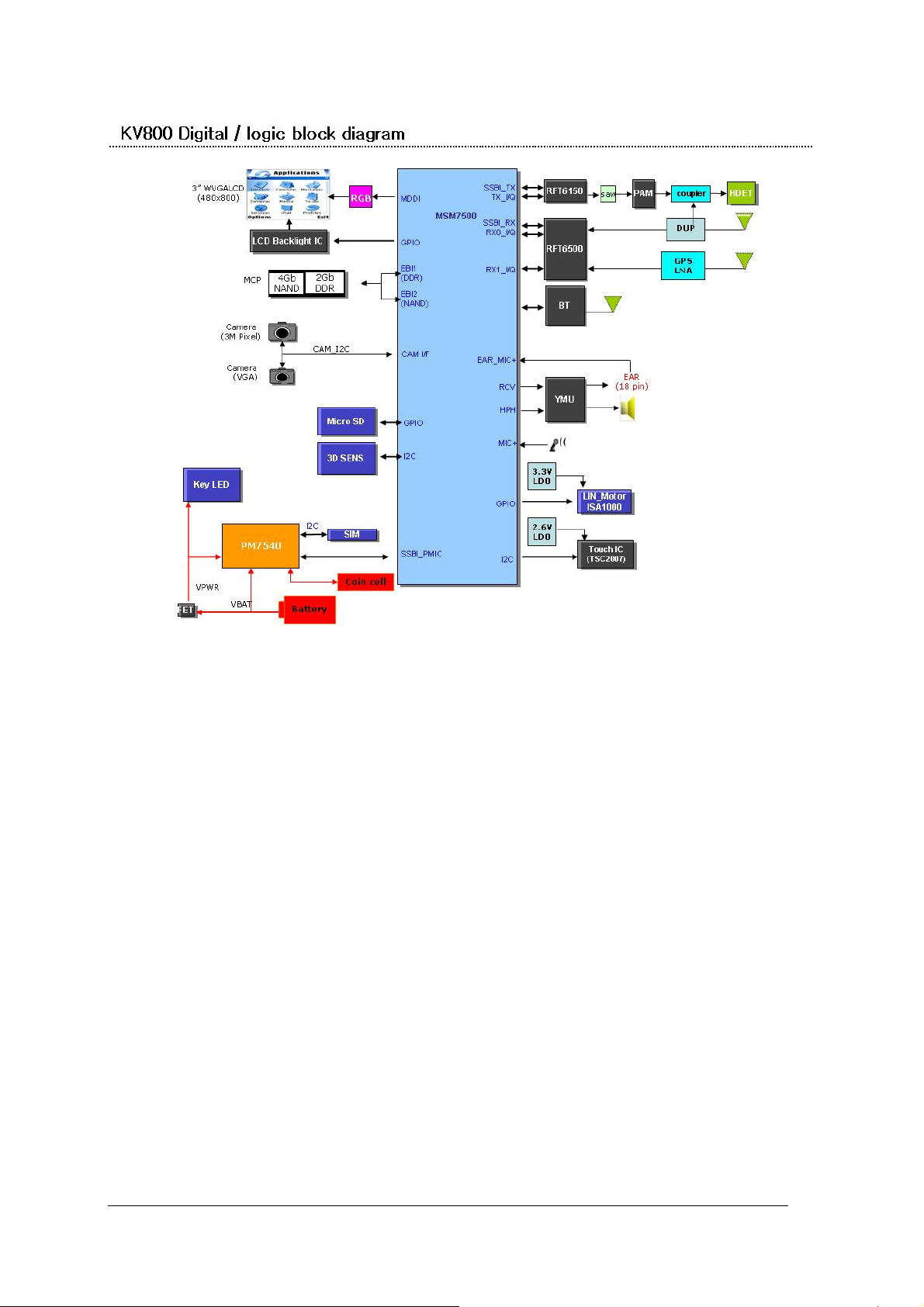
[Figure 2-2] Block Diagram of Digital/ Logic Processing Part
3.2.3.4 Memory Part
MCP contents 1 Gbits flash memory and 1Gbit user memory and 1 Gbits SDRAM. In the Flash Memory part of
MCP are programs used for terminal operation. The programs can be changed through down loading after the
assembling of terminals. On the SDRAM data generated during the terminal operation are stored temporarily.
3.2.3.5 Power Supply Part
When the battery voltage (+4.0V) is fed and the PWR key of keypad is pressed, the power-up circuitry in PM
(power management) IC (U4300) is activated by the ON_SW signal, and then the LDO regulators embedded in
PMIC for MSM) are operated and +1.2V_MSMC1, +1.2V_MSMC2, +2.6V_MSMP3, +2.6V_MSMA and
+1.8V_MSME_P4 are generated.
The Rx part regulator (+2.85V_RX) is operated by the control signal of SLEEP/ from MSM7500-1
The Tx part regulator (+2.85V_TX) is operated by the I2C control signal from MSM7500-1
Copyright©2009 LG Electronics. Inc. All right reserved. LGE Internal Use Only
Only for training and service purpose.
19

3.2.3.6 Logic Part
The logic part consists of internal CPU of MSM, RAM, MCP. The MSM7500-1 receives TCXO (=19.2MHz)
from U1008 and controls the phone in CDMA mode. The major components are as follows:
z
CPU
The ARM926EJ-S microprocessor includes a 3 stage pipelined RISC architecture, both 32-bit ARM and 16-bit
THUMB instruction sets, a 32-bit address bus, and a 32-bit internal data bus. It has a high performance and low
power consumption.
MCP
z
Flash ROM is used to store the terminal’s program. Using the down-loading program, the program can be
changed even after the terminal is fully assembled.
SDRAM is used to store the internal flag information, call processing data, and timer data.
z
Touch
Touch window is transmit Touch signals to MSM7500-1 via touch control IC (Sub PCB U1500)
Copyright©2009 LG Electronics. Inc. All right reserved. LGE Internal Use Only
Only for training and service purpose.
20

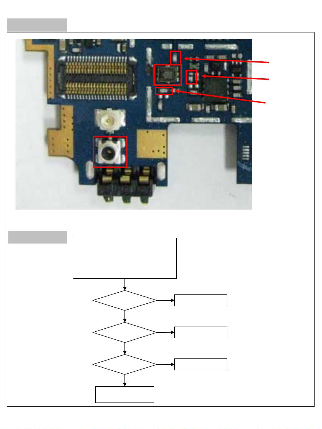
CHAPTER 4. Trouble shooting
CHAPTER 4. Trouble shooting
4.1 Rx Part Trouble
4.1.1 When Rx Power isn’t enough
Test Point
RFR6500
RX SAW
Duplexer
TCXO
PMIC Part
Mobile s /w
Checking Flow
Rx TEST SETUP(HHP)
- Test Channel : 384
E5515C Setup
- CH : 384
- Sector Power : -30 dBm
Spectrum Analyzer Setting
Oscilloscope Setting
START
1.Check
PMIC Circuit
2.Check
TCXO Circuit
Figure 1
4.Check LNA, RX SAW
5.Check
Control Signal
6.Check
Rx I/Q data
3.Check
Duplexer
Mobile SW
Copyright©2009 LG Electronics. Inc. All right reserved. LGE Internal Use Only
Only for training and service purpose
- 21 -
Redownload SW, CAL

4.1.2 Checking Regulator (PMIC) Circuit
Test Point
U4300
PMIC
Circuit Diagram
R4302 Up Pad
(PS_HOLD)
R4318 (+2.85V_RX)
Figure 2
Checking Flow
Check R4318
+2.85V_Rx OK?
Yes Yes
PMIC Circuit is OK
See next Page to check
TCXO
No
- 22 -
Check R4318
Up Pad
PS_HOLD High?
Replace U4300
No
Changing Board

4.1.3 Checking TCXO Circuit
Test Point Checking Flow
R1303
(TCXO)
R1301
(+2.85V_TCXO)
Circuit Diagram
TCXO
U1008
U1008
R1303
19.2MHz OK?
NO
R1301
2.85V OK?
NO
Check U4300(PMIC)
Figure 3
YES
YES
TCXO Circuit is OK
See next page to check
SBI control signal
Replace U1008
Waveform
Figure 4:
Copyright©2009 LG Electronics. Inc. All right reserved. LGE Internal Use Only
Only for training and service purpose
R1303 TCXO
- 23 -
Figure 5:
R1301 +2.85V_TCXO
4.1.4 Check Mobile S/W & Diplexer & Duplexer
Test Point
DP1001
Duplexer
U1001
M/S
C1508
(P1 : RFOUT to RX)
L1007
(P2 : RFIN From TX)
C1006
(P3 : RFOUT to M/S)
Checking Flow
Check C1006
Check C1508
Check L1007
Rx TEST SETUP(HHP)
- Test Channel : 384(DCN)
E5515C Setup
- CH : 384(DCN)
- Sector Power : -30 dBm
Spectrum Analyzer Setting
Oscilloscope Setting
Level is Appear?
YES
Level is Appear?
YES
Level is Appear?
YES
Figure 6
NO
Replace U1001
NO
Replace DP1001
NO
Replace DP1001
Redownload SW and
Recalibration
Copyright©2009 LG Electronics. Inc. All right reserved. LGE Internal Use Only
Only for training and service purpose
- 24 -

4.1.4 Check Mobile S/W & Diplexer & Duplexer
Circuit Diagram
Waveform
C1508
Figure 7
- 25 -
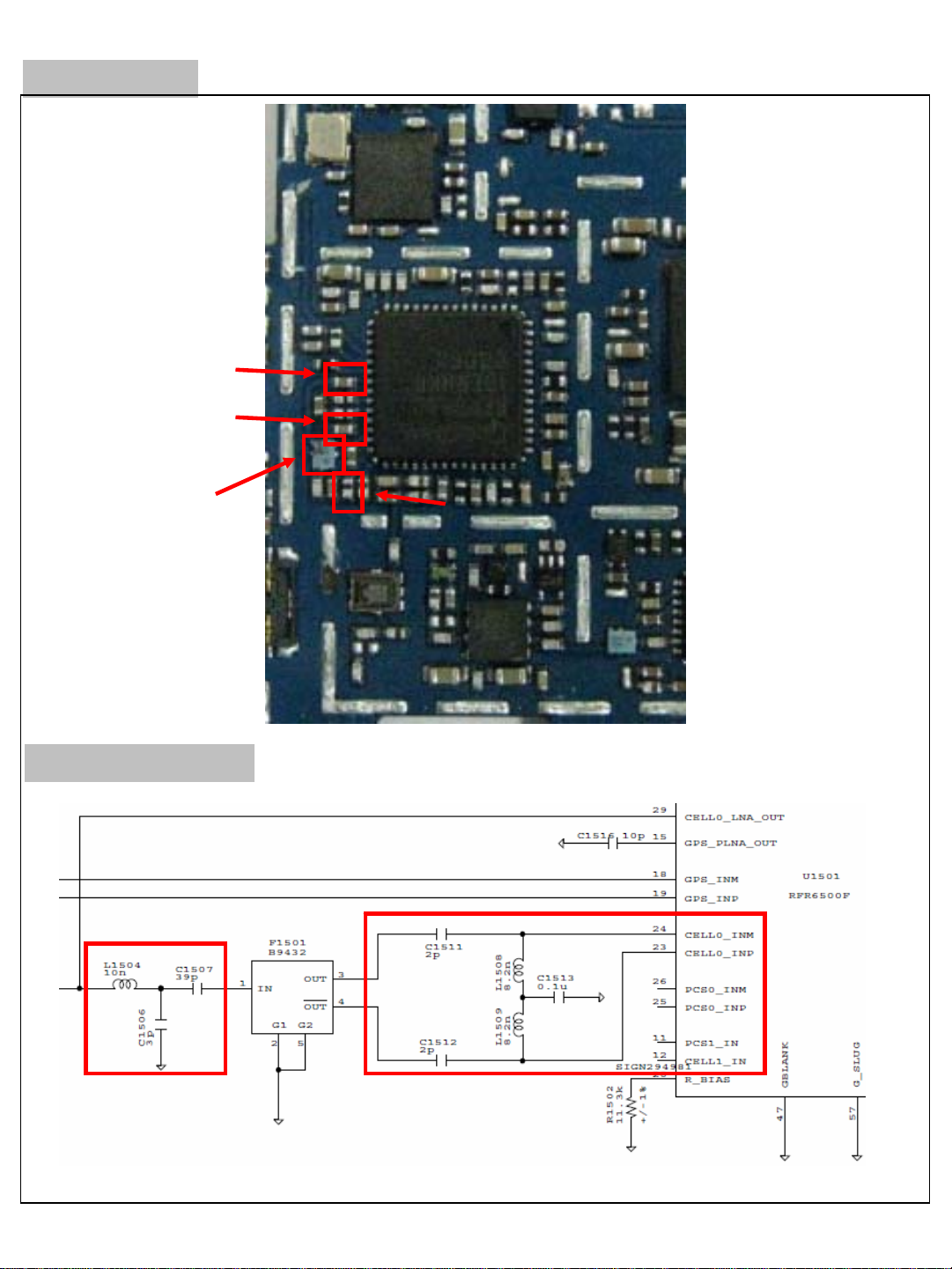
4.1.5 Checking LNA & SAW (DCN,PCS)
Test Point
C1512
CELL_INP
C1511
CELL_INM
F1501
SAW Filter
Circuit Diagram
U1501
RFR6500
L1504
CLNA_OUT
Figure 8
Copyright©2009 LG Electronics. Inc. All right reserved. LGE Internal Use Only
Only for training and service purpose
- 26 -

4.1.5 Checking LNA & SAW (DCN,PCS)
Checking Flow
Rx TEST SETUP(HHP)
- Test Channel : 384(DCN)
E5515C Setup
- CH : 384(DCN)
- Sector Power : -30 dBm
Spectrum Analyzer Setting
Oscilloscope Setting
waveform
Check LNA,
L1504 (RFR6500)
Check SAW, C1511,C1512)
Detected Signal? Changing U1501
Yes
Detected Signal?
Yes
See next Page to check
Rx I/Q data Signal
No
No
Changing F1501
Figure 9
Copyright©2009 LG Electronics. Inc. All right reserved. LGE Internal Use Only
Only for training and service purpose
- 27 -
 Loading...