

LG KC560 Service Manual
Service Manual
Model : KC560
Service Manual
KC560
Date: November, 2008 / Issue 1.0
Internal Use Only
REVISED HISTORY
J
Editor Date Issue Contents of Changes S/W Version
.G.PARK 6/02 0.1
* The information in this manual is subject to change without notice and should not be
construed as a commitment by LGE Inc. Furthermore, LGE Inc. reserves the right, without
notice, to make changes to equipment design as advances in engineering and manufacturing
methods warrant.
This manual provides the information necessary to install, program, operate and
maintain the KC560.
Copyright © 2008 LG Electronics. Inc. All right reserved.
Only for training and service purposes
- 3 -
LGE Internal Use Only

LGE Internal Use Only Copyright © 2008 LG Electronics. Inc. All right reserved.
- 4 -
Only for training and service purposes

Table Of Contents
1. INTRODUCTION ...............................................9
1.1 Purpose ......................................................................9
1.2 Regulatory Information .................................................9
2. PERFORMANCE .............................................11
2.1 H/W Feature..............................................................11
2.2 Technical specifi cation ...............................................13
3. TECHNICAL BRIEF .........................................19
3.1 KC560 Functional Block diagram ...............................19
3.2 Baseband Processor (BBP) Introduction ......................20
3.3 Power management IC...............................................29
3.4 Power ON/OFF ..........................................................34
3.5 SIM & uSD interface ..................................................35
3.6 Memory ....................................................................37
3.7 LCD Display ..............................................................38
3.8 Keypad Switching & Scanning ....................................39
3.9 Keypad back-light illumination ....................................40
3.10 LCD back-light illumination ......................................41
3.11 ALC ........................................................................42
3.12 Battery current consumption monitor ........................43
3.13 JTAG & ETM interface connector ..............................43
3.14 Audio ......................................................................44
3.15 charging circuit .......................................................45
3.16 FM radio & BLUETOOTH...........................................46
3.17 18pin Multi Media Interface connector ......................49
3.18 General Description .................................................50
3.19 Receiver part ...........................................................52
3.20 Transmitter part .......................................................52
3.21 RF synthesizer .........................................................53
3.22 DCXO .....................................................................53
3.23 Front End Module control .........................................54
3.24 Power Amplifi er Module ...........................................54
3.25 Mode Selection .......................................................55
3.26 PAM Schematic .......................................................56
4. PCB layout .................................................... 57
4.1 Main & Sub PCB component placement ......................57
5.3 Charging trouble........................................................65
5.4 LCD display trouble ...................................................67
5.5 Camera Trouble .........................................................69
5.6 Receiver & Speaker trouble ........................................71
5.7 Microphone trouble ...................................................73
5.8 Vibrator trouble ..........................................................74
5.9 Keypad back light trouble ...........................................75
5.10 SIM & uSD trouble ...................................................76
5.11 Photo sensor trouble ................................................79
5.12 RGB LED trouble ......................................................80
5.13 Trouble Shooting of Receiver Part .............................81
5.14 Trouble Shooting of Transmitter Part .........................87
6. Multi-Download ........................................... 96
7. BLOCK DIAGRAM ........................................ 100
8. CIRCUIT DIAGRAM ...................................... 101
9. BGA Pin Map .............................................. 109
10. PCB LAYOUT .............................................111
11. RF Calibration .......................................... 121
11.1 Test Equipment Setup ............................................121
11.2 Calibration Step .....................................................121
12. STAND-ALONE TEST ................................. 126
12.1 Test Program Setting .............................................126
12.2 Tx Test ..................................................................128
12.3 Rx Test ..................................................................129
13. ENGINEERING MODE .................................131
14. EXPLODED VIEW & REPLACEMENT
PART LIST ................................................. 133
14.1 EXPLODED VIEW ...................................................133
14.2 Replacement Parts ................................................135
14.3 Accessory .............................................................157
5. TROUBLE SHOOTING ..................................... 61
5.1 Trouble shooting test setup ........................................61
5.2 Power on Trouble .......................................................62
Copyright © 2008 LG Electronics. Inc. All right reserved.
Only for training and service purposes
- 5 -
LGE Internal Use Only

LGE Internal Use Only Copyright © 2008 LG Electronics. Inc. All right reserved.
- 6 -
Only for training and service purposes
ABBREVIATION
G
G G G G G GG
For the purposes of this manual, following abbreviations apply:
APC Automatic Power Control
BB Baseband
BER Bit Error Ratio
CC-CV Constant Current – Constant Voltage
CLA Cigar Lighter Adapter
DAC Digital to Analog Converter
DCS Digital Communication System
dBm dB relative to 1 milli-watt
DSP Digital Signal Processing
EEPROM Electrical Erasable Programmable Read-Only Memory
EGPRS
EL Electroluminescence
ESD Electrostatic Discharge
FPCB Flexible Printed Circuit Board
GMSK Gaussian Minimum Shift Keying
GPIB General Purpose Interface Bus
GPRS General Packet Radio Service
GSM Global System for Mobile Communications
IPUI International Portable User Identity
IF Intermediate Frequency
LCD Liquid Crystal Display
LDO Low Drop Output
LED Light Emitting Diode
LGE LG Electronics
OPLL Offset Phase Locked Loop
PAM Power Amplifier Module
PCB Printed Circuit Board
PGA Programmable Gain Amplifier
PLL Phase Locked Loop
PSTN Public Switc hed Te lephone Network
RF Radio Frequency
RLR Receiving Loudness Rating
RMS Root Mean Square
RTC Real Time Clock
SAW Surface Acoustic Wave
SIM Subscriber Identity Module
SLR Sending Loudness Rating
lGnGwGyGzG
Copyright © 2008 LG Electronics. Inc. All right reserved.
Only for training and service purposes
- 7 -
LGE Internal Use Only

SRAM Static Random Access Memory
STMR Side Tone Masking Rating
TA Travel Adapter
TDD Time Division Duplex
TDMA Time Division Multiple Access
UART Universal Asynchronous Receiver/Transmitter
VCO Voltage Controlled Oscillator
DCXO Digitally Controlled Crystal Oscillator
WAP Wireless Application Protocol
8PSK 8 Phase Shift Keying
LGE Internal Use Only Copyright © 2008 LG Electronics. Inc. All right reserved.
- 8 -
Only for training and service purposes

1. INTRODUCTION
1. INTRODUCTION
1.1. Purpose
This manual provides the information necessary to repair, calibration, description and
download the features of the
1.2. Regulatory Information
1.2.1. Security
Toll fraud, the unauthorized use of telecommunications system by an unauthorized part (for
example, persons other than your company’s employees, agents, subcontractors, or person
working on your company’s behalf) can result in substantial additional charges you’re your
telecommunications services. System users are responsible for the security of own system.
There are may be risks of toll fraud associated with your telecommunications system. System
users are responsible for programming and configuring the equipment to prevent unauthorized
use. LGE does not warrant that this product is immune from the above case but will prevent
unauthorized use of common-carrier telecommunication service of facilities accessed through
or connected to it. LGE will not be responsible for any charges that result from such
unauthorized use.
KC560.
1.2.2. Incidence of Harm
If a telephone company determines that the equipment provided to customer is faulty and
possibly causing harm or interruption in service to the telephone network, it should disconnect
telephone service until repair can be done. A telephone company may temporarily disconnect
service as long as repair is not done.
1.2.3. Changes in Service
A local telephone company may make changes in its communications facilities or procedure.
If these changes could reasonably be expected to affect the use of the
with the network, the telephone company is required to give advanced written notice to the
user, allowing the user to take appropriate steps to maintain telephone service.
KC560 or compatibility
1.2.4. Maintenance Limitations
Maintenance limitations on the KC560 must be performed only at the LGE or its authorized
agents. The user may not make any changes and/or repairs expect as specifically noted in this
manual. Therefore, note that unauthorized alternations or repair may affect the regulatory
status of the system and may void any remaining warranty.
1.2.5. Notice of Radiated Emissions
The KC560 complies with rules regarding radiation and radio frequency emission as defined
by local regulatory agencies. In accordance with these agencies, you may be required to
provide information such as the following to the end user.
Copyright © 2008 LG Electronics. Inc. All right reserved.
Only for training and service purposes
- 9 -
LGE Internal Use Only

1. INTRODUCTION
1.2.6. Pictures
The pictures in this manual are for illustrative purposes only; your actual hardware may look
slightly different.
1.2.7. Interference and Attenuation
The KC560 may interfere with sensitive laboratory equipment, medical equipment, etc.
Interference from unsuppressed engines or electric motors may cause problems.
1.2.8. Electrostatic Sensitive Devices
ATTENTION
Boards, which contains Electrostatic Sensitive Device(ESD), are indicated by the sign.
Following information is ESD handling: Service personnel shou ld ground themselves by using
a wrist strap when exchange system boards.
When repairs are made to a system b oard, they should spread the floor with anti-static mat
which is also grounded. Use a suitable, grounded soldering iron . Keep sensitive parts in these
protective packages until these are used. When returning system boards or parts such as
EEPROM to the factory, use the protective package as described.
LGE Internal Use Only Copyright © 2008 LG Electronics. Inc. All right reserved.
- 10 -
Only for training and service purposes
2. PERFORMANCE
2.1 H/W Feature
Item Feature Comment
Form Factor
2. PERFORMANCE
Slide
Battery
Size Standard :
Weight TBD With Battery
Volume ??cc
PCB Staggered 10Layers , 0.8t
Stand by time 250 hrs @ Paging Period 9
Charging time 3 hrs @ Power Off / 900mAh
Talk time Min : 3.0 hrs @ Power Level 7 @ EGSM / 900mAh
RX sensitivity EGSM : -105 dBm
TX output power
GPRS compatibility GPRS Class 10
EDGE compatibility EDGE Class 10
SIM card type Plug-In SIM
GSM/
GPRS
EDGE EGSM : 26 dBm
1) Capacity
Standard : Li-Ion, 900mAh
2) Packing Type : Soft Pack
103.8 X 51.4 X 14.9 mm
DCS 1800 : -105 dBm
PCS 1900 : -105 dBm
EGSM : 32.7 dBm
DCS 1800 : 31dBm
PCS 1900 : 30 dBm
DCS 1800 : 25 dBm
PCS 1900 : 25 dBm
3V /1.8V
Class4 (EGSM)
Class1 (PCS)
Class1 (DCS)
E2 (EGSM)
E2 (PCS)
E2 (DCS)
Copyright © 2008 LG Electronics. Inc. All right reserved.
Only for training and service purposes
- 11 -
LGE Internal Use Only
2. PERFORMANCE
Display 1. Main LCD
2. 262K Color TFT (320 x 240)
Backlight : White LED
Built-in Camera
Status Indicator
Keypad Alphanumeric Key : 12
ANT Main : Internal Fixed Type
System connector 18 Pin
Ear Phone Jack 18pin, Stereo
PC synchronization Yes
Memory NAND Flash : 1Gbit
Speech coding FR, EFR, HR,AMR
Data & Fax Built in Data & Fax support
Vibrator Built in Vibrator
Blue Tooth V2.1
MIDI(for Buzzer
Function)
Music Player MP3/ WMA/AAC/AAC+/AAC++ With Graphic EQ
Video Player MPEG4, H.263,
3M CMOS Camera (QXGA) One button access
None
Function Key:
Function Key : 10
Side Key : 4
Total No of Keys :26
SDRAM : 512Mbit
64Poly , MP3 ringtone
4 Key Navigation, OK, F1, F2, CLR,
SND, END
Side Key :
Jog wheel, CAM, Task
Camcorder MPEG4, H.263,
Voice Recording Yes
Speaker Phone mode
Support
Travel Adapter Y es
CDROM No
Stereo Headset Yes
Data Cable No
T-Flash(External Memory) No
LGE Internal Use Only Copyright © 2008 LG Electronics. Inc. All right reserved.
Yes
- 12 -
Only for training and service purposes
2.2 Technical specification
Item Description Specification
GSM900
1) PGSM
TX: 890 + 0.2 x n MHz
RX: 935 + 0.2 x n MHz ( n = 1 ~ 124 )
2) EGSM
TX: 890 + 0.2 x (n-1024) MHz
1 Frequency Band
2 Phase Error
3 Frequency Error < 0.1ppm
4 Power Level
5 Output RF Spectrum
( due to modulation)
RX: 935 + 0.2 x (n-1024) MHz ( n = 975 ~ 1023 )
DCS1800
TX: 1710.2 + 0.2 x (n-512) MHz
RX: 1805.2 + 0.2 x (n-512) MHz (n = 512 ∼ 885)
PCS1900
TX: 1850 + ( n-511 ) × 0.2 MHz
RX: 1930 + ( n-511 ) × 0.2 MHz (n = 512 ∼ 810)
RMS < 5 degrees,
Peak < 20 degrees
GSM900
Level Power Toler. Level Power Toler.
5 33 dBm –2dB 13 17 dBm –3dB
6 31 dBm –3dB 14 15 dBm –3dB
7 29 dBm –3dB 15 13 dBm –3dB
8 27 dBm –3dB 16 11 dBm –5dB
9 25 dBm –3dB 17 9 dBm –5dB
10 23 dBm –3dB 18 7 dBm –5dB
11 21 dBm –3dB 19 5 dBm –5dB
12 19 dBm –3dB
DCS / PCS
Level Power Toler. Level Power Toler.
0 30 dBm –2dB 8 14 dBm –3dB
1 28 dBm –3dB 9 12 dBm –4dB
2 26 dBm –3dB 10 10 dBm –4dB
3 24 dBm –3dB 11 8 dBm –4dB
4 22 dBm –3dB 12 6 dBm –4dB
5 20 dBm –3dB 13 4 dBm –4dB
6 18 dBm –3dB 14 2 dBm –5dB
7 16 dBm –3dB 15 0 dBm –5dB
GSM900
Offset from Carrier (kHz). Max. dBc
100 +0.5
200 -30
2. PERFORMANCE
Copyright © 2008 LG Electronics. Inc. All right reserved.
Only for training and service purposes
- 13 -
LGE Internal Use Only
2. PERFORMANCE
6
7 Spurious Emissions
8 Bit Error Ratio
9 Rx Level Report accuracy
10 SLR
11 Sending Response
Output RF Spectrum
(due to switching)
250 -33
400 -60
600 ~ 1,200 -60
1,200 ~ 1,800 -60
1,800 ~ 3,000 -63
3,000 ~ 6,000 -65
6,000 -71
DCS / PCS
Offset from Carrier (kHz). Max. dBc
100 +0.5
200 -30
250 -33
400 -60
600 ~ 1,200 -60
1,200 ~ 1,800 -60
1,800 ~ 3,000 -65
3,000 ~ 6,000 -65
6,000 -73
GSM900
Offset from Carrier (kHz) Max. (dBm)
400 -19
600 -21
1,200 -21
1,800 -24
DCS / PCS
Offset from Carrier (kHz) Max. (dBm)
400 -22
600 -24
1,200 -24
1,800 -27
Conduction, Emission Status
Conduction, Emission Status
GSM900
BER (Class II) < 2.439% @-102dBm
DCS / PCS
BER (Class II) < 2.439% @-102dBm
± 3 dB
8 ± 3 dB
Frequency (Hz) Max.(dB) Min.(dB)
100 -12 /
200 0 /
LGE Internal Use Only Copyright © 2008 LG Electronics. Inc. All right reserved.
- 14 -
Only for training and service purposes
300 0 -12
1,000 0 -6
2,000 4 -6
3,000 4 -6
3,400 4 -9
4,000 0 /
12 RLR
13 Receiving Response
14 STMR > 17 dB
15 Echo Loss > 44 dB
16 Idle Noise Sending < -64 dBm0p
17 Idle Noise Receiving < -54 dBm0p
2 ± 3 dB
Frequency (Hz) Max.(dB) Min.(dB)
100 -6 /
200 2 /
300 2 -9
1,000 2 -7
3,400 2 -12
4,000 2
2. PERFORMANCE
<Change> System
18
19
20 Power consumption
21 Talk Time
22 Standby Time
23 Ringer Volume
24 Charge Voltage Fast Charge : < 500 mA
frequency
(13 MHz) tolerance
<Change>32.768KHz
tolerance
≤ 2.5ppm
≤ 30ppm
Full power
< 340mA (GSM900) ; < 260mA (DCS / PCS)
Standby
- Normal Mode ≤ 4.0mA(Max. power)
- Using Test mode on DSP Sleep function ≤ 6mA
GSM900/Level7 (Battery 900mA):230 Min
GSM900/Level12(Battery 900mA):390 Min
PCS1800/Level5 (Battery 900mA):340 Min
PCS1800/Level10(Battery 900mA):430 Min
Under conditions, at least 250 hours:
Brand new and full 900mAh battery
Full charge, no receive/send and keep GSM
in the mode. Broadcast set off.
Signal strength display set at 3 level above.
Backlight of phone set off.
At least 55 dB under below conditions:
1. Ringer set as ringer.
2. Test distance set as 1 m
Copyright © 2008 LG Electronics. Inc. All right reserved.
Only for training and service purposes
- 15 -
LGE Internal Use Only
2. PERFORMANCE
Slow Charge: < 120 mA
Antenna Bar Number Power
25 Antenna Display
26 Battery Indicator
27 Low Voltage Warning
28 Forced shut down Voltage
29 Battery Type
7->5
5->4
4->2
2->1
1->0
-93¡ 3dBm
-98¡ 3dBm
-101¡ 3dBm
-104¡ 3dBm
-106¡ 3dBm
Battery Bar Number Voltage
Cut Off 3.20V ~ 3.30V (3.25V)
1->Blinking 3.50V ~ 3.60V (3.55V)
2->1 3.58V ~ 3.68V (3.63V)
3->2 3.68V ~ 3.78V (3.73V)
3 ~ 4.20V
Call, Blinking Voltage 3.52V ~ 3.62V (3.57V)
3.57 ¡ 0.05 V (Call / Warning tone once per one minutes)
3.55 ¡ 0.05 V (Standby /
Warning tone once per three minutes)
3.25 ¡ 0.05 V
Li-Ion Battery, Soft pack,
Standard Voltage = 3.7 V
Battery full charge voltage = 4.2 V,
Capacity: 900mAh
30 Travel Charger
Switching-mode charger
Input: 100 ∼ 240 V , 50/60H z
Out put: 5.1V, 700mA
LGE Internal Use Only Copyright © 2008 LG Electronics. Inc. All right reserved.
- 16 -
Only for training and service purposes
p(p )
EDGE RF Specifi cation (Option: is not serviced for ”EDGE mode”)
Item Description Specification
1 RMS EVM 9%
2 Peak EVM 30%
3 95th Percentile EVM 15%
4 Origin Offset Suppression 30dB
GSM900/EGSM
Level Power Toler. Level Power Toler.
5 26dBm –3dB 13 17dBm –3dB
6 26dBm –3dB 14 15dBm –3dB
7 26dBm –3dB 15 13dBm –3dB
8 25dBm –3dB 16 11dBm –5dB
9 25dBm –3dB 17 9dBm –5dB
10 23dBm –3dB 18 7dBm –5dB
11 21dBm –3dB 19 5dBm –5dB
5 Power Level
6 Output RF Spectrum
(due to modulation)
12 19dBm –3dB
DCS1800, PCS1900
Level Power Toler. Level Power Toler.
0 25/25dBm –3dB 8 14dBm –3dB
1 25/25dBm –3dB 9 12dBm –4dB
2 25/25dBm –3dB 10 10dBm –4dB
3 24dBm –3dB 11 8dBm –4dB
4 22dBm –3dB 12 6dBm –4dB
5 20dBm –3dB 13 4dBm –4dB
6 18dBm –3dB 14 2dBm –5dB
7 16dBm –3dB 15 0dBm –5dB
GSM900/EGSM
Offset from carrier(kHz) Max. dBc
100 +0.5
200 -30
250 -33
400 -54
600~<1,200 -60
1,200~<1,800 -60
1,800~<3,000 -63
3,000~<6,000 -65
6,000 -71
DCS1800, PCS1900
Offset from carrier(kHz) Max. dBc
100 +0.5
200 -30
250 -33
400 -54
2. PERFORMANCE
Copyright © 2008 LG Electronics. Inc. All right reserved.
Only for training and service purposes
- 17 -
LGE Internal Use Only
2. PERFORMANCE
Output RF Spectrum
7
(due to switching transient)
600~<1,200 -60
1,200~<1,800 -60
1,800~<3,000 -63
3,000~<6,000 -65
6,000 -71
GSM900/EGSM
Offset from carrier(kHz) Max. dBm
400 -23
600 -26
1,200 -27
1,800 -30
DCS1800, PCS1900
Offset from carrier(kHz) Max. dBm
400 -23
600 -26
1,200 -27
1,800 -30
LGE Internal Use Only Copyright © 2008 LG Electronics. Inc. All right reserved.
- 18 -
Only for training and service purposes
3. TECHNICAL BRIEF
III-1 Baseband circuit
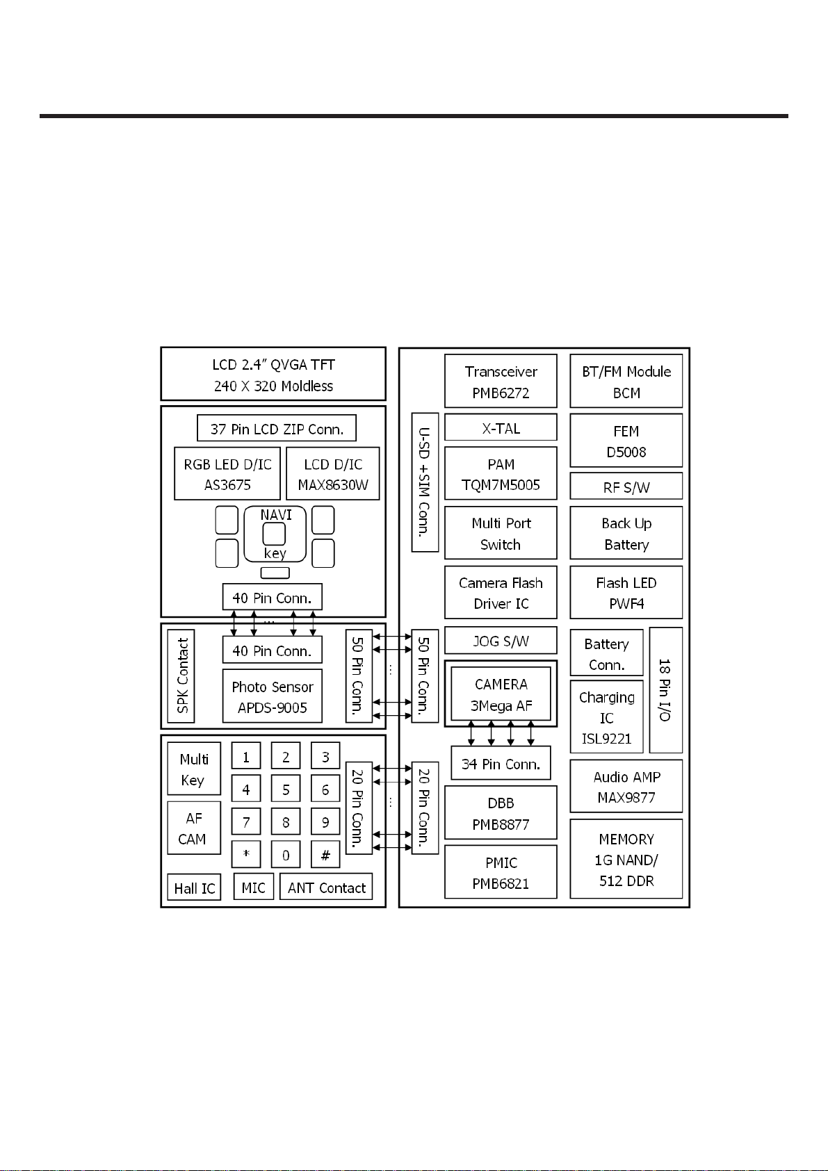
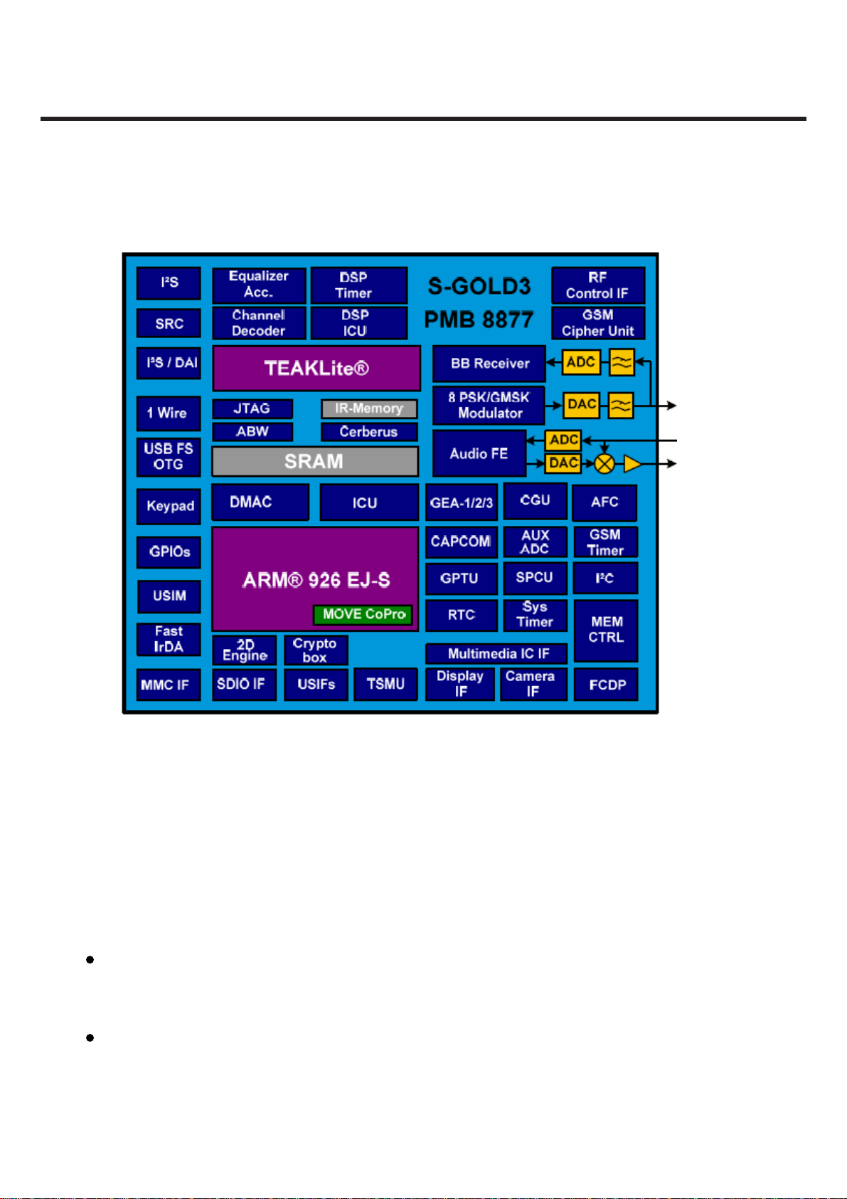
3.1. KC560 Functional Block diagram.
The functional component arrangement is mentioned below diagram.
3. TECHNICAL BRIEF
Figure 2 KC560 Functional block diagram
Copyright © 2008 LG Electronics. Inc. All right reserved.
Only for training and service purposes
- 19 -
LGE Internal Use Only
3. TECHNICAL BRIEF
3.2. Baseband Processor (BBP) Introduction
Figure 3 Top level block diagram of the S-GOLD3TM (PMB8877)
3.2.1. General Description
S-GOLD3TM is a GSM/EDGE single chip mixed signal Baseband IC containing all analog and digital
functionality of a cellular radio. Additionally S-GOLD3
software MIDI, MP3 sound. It is designed as a single chip solution, integrating the digital and mixed
signal portions of the base band in 0.09um, 1.2V technology.
The chip will fully support the FR, EFR, HR and AMR-NB vocoding.
S-GOLD3
application (up to class 12) and EGPRS (up to class 12) without additional external hardware.
TM
support multi-slot operation modes HSCSD (up to class 10), GPRS for high speed data
TM
Provides multimedia extensions such as camera,
3.2.2. Block Description
Processing core
ARM926EJ-S 32 bit processor core for controller functions. The ARM926EJ-S includes an MMU, and
the Jazelle Java extension for Java acceleration.
- TEAKLite DSP core
ARM-Memory
- 32k Byte Boot ROM on the AHB
- 96k Byte SRAM on the AHB, flexibly usable as program or data RAM
- 16k Byte Cache for Program (internal)
LGE Internal Use Only Copyright © 2008 LG Electronics. Inc. All right reserved.
- 20 -
Only for training and service purposes

3. TECHNICAL BRIEF
- 8k Byte tightly coupled memory for Program(internal)
- 8k Byte Cache for Data(internal)
- 8k Byte tightly coupled memory for Data(internal)
DSP-Memory
- 104K x 16bit Program ROM
- 8k x 16bit Program RAM
- 60k x 16bit Data ROM
- 37k x 16bit Data RAM
- Incremental Redundancy(IR) Memory of 35904 words of 16bit
Shared Memory Block
1.5K x 32bit Shared RAM(dual ported) between controller system and TEAKLite.
Controller Bus system
The processor cores and their peripherals are connected by powerful buses.
Multi-layer AHB for connecting the ARM and the other master capable building blocks with the internal
and external memories and with the peripheral buses.
Clock system
The clock system allows widely independent selection of frequencies for the essential parts of the
S-GOLD3. Thus power consumption and performance can be optimized for each application.
Functional Hardware block
- CPU and DSP Timers
- MOVE coprocessor performing motion estimation for video encoding algorithms
(H.263, MPEG-4)
- Programmable PLL with additional phase shifters for system clock generation
- GSM Timer Module that off-loads the CPU from radio channel timing
- GMSK / 8-PSK Modulator according to GSM-standard 05.04 (5/2000)
- GMSK Modulator: gauss-filter with B*T=0.3
- EDGE Modulator: 8PSK-modulation with linearized GMSK-Pulse-Filter
- Hardware accelerators for equalizer and channel decoding.
- Incremental Redundancy memory for EDGE class 12 support
- A5/1, A5/2, A5/3 Cipher unit
- GEA1, GEA2, GEA3 Cipher Unit to support GPRS data transmission
- Advanced static and dynamic power management features including TDMA-Frame
synchronous low power mode and enhanced CPU modes(idle and sleep modes)
- Pulse Number Modulation output for Automatic Frequency Correction(AFC)
- Serial RF Control interface: support of direct conversion RF
- A Universal Serial Interface(USIF) enabling asynchronous (UART) of synchronous (SPI)
serial data transmission
- 3 USIF with auto baud detection, hardware flow control and integrated
- A dedicated Fast IrDA Controller supporting IrDAs SIR,MIR and FIR standards
(up to 4Mbps)
- I2C-bus interface (e.g. connection to S/M power)
- A fast display interface supporting serial and parallel interconnection
- An ITU-R BT.656 compatible Camera interface.
- Programmable clock output for a camera
- An multimedia/Secure Digital Card Interface (MMCI/SD:SDIO capable)
Copyright © 2008 LG Electronics. Inc. All right reserved.
Only for training and service purposes
- 21 -
LGE Internal Use Only
3. TECHNICAL BRIEF
3.2.3. External Devices connected to memory interface
Table 1. Memory interface
Device Name Maker Remark
FLASH K5E1H12ACM-D075 Samsung Synchronous / A synchronous
DDR K5E1H12ACM-D075 Samsung Synchronous 133MHz
LCD
CAMERA C3AA-M197B
IM240DBNCA
3.2.4. RF Interface (T_OUT)
S-Gold3 uses this interface to control RF IC and Per ipherals. 13 signals are provided switch on/off RF
ICs Periodically each TDMA frame.
Table 2. RF Interface Spec.
LGIT 16bit access
LGIT
8bit data Interface
T_OUT
Resource Interconnection Description
T_OUT0 TXON_PA PAM Power on
T_OUT1 FE2 FEM control
T_OUT2 PA_BAND TX RF band select
T_OUT3 FE1 FEM control
T_OUT4 Other operation -
T_OUT5 Other operation -
T_OUT6 PA MODE PAM Mode select
3.2.5. USIF Interface
KC560 have three USIF Drivers as follow :
- USIF1 : Hardware Flow Control / SW upgrade / Calibration
- USIF2 : MON used Rx, Tx and CTS, RTS use BT Interface
- USIF3 : BT Interface
Table 3. USIF Interface Spec.
Resource Name Remark
USIF1
USIF1_TXD UART_TX Transmit Data
USIF1_RXD UART_RX Receive Data
USIF1_CTS USB_SE0_VM
USIF1_RTS USB_DAT_VP
USIF2
USIF2_TXD N.C
USIF2_RXD N.C
USIF2_CTS UART_BT_CTS
USIF2_RTS UART_BT_RTS.
USIF3
USIF3_TXD UART_BT_TX BT Transmit tx
USIF3_RXD UART_BT_RX BT Receive rx
,
LGE Internal Use Only Copyright © 2008 LG Electronics. Inc. All right reserved.
- 22 -
Only for training and service purposes
3. TECHNICAL BRIEF
3.2.6. ADC channel
BBP ADC block is composed of 7 external ADC channel. This block operates charging process and
other related process by reading battery voltage and other analog values.
Table 4. S-Gold3 ADC channel usage
ADC channel
Resource Interconnection Description
M0 BAT_ID Battery temperature measure
M1 RF_TEMP RF block temperature measure
M2 REMOTE_ADC Remote Control
M3 JACK_TYPE Accessory type detect
M4 N.C
M5 2V62_VIO PCB revision
M6 N.C
M7 N.C
M8 VSUPPLY Battery supply voltage measure
M9 LOAD Current consumption measure
M10 N.C
3.2.7. GPIO map
Over a hundred allowable resources, KC560 is using as fo llows except dedicated to SIM and Memory.
KC560 GPIO(General Purpose Input/Output) Map, describing application, I/O state, and enable level, is
shown in below table
Table 5 S-Gold3 GPIO pin Map
Port Function Net Name Description
KEY MATRIX
KP_IN0
KP_IN1
KP_IN2
KP_IN3
KP_IN4
KP_IN5
KP_IN6
KP_OUT0
KP_OUT1
KP_OUT2
KP_OUT3
USIF1
USIF1_RXD
USIF1_TXD
USIF1_RTS_N
USIF1_CTS_N
USIF2
USIF2 _RXD
KP_ROW0
KP_ROW1
KP_ROW2
KP_ROW3
KP_ROW4
KP_ROW5
KP_ROW6
KP_COL0
KP_COL1
KP_COL2
KP_COL3
RXD UART, RS232 Data
TXD UART, RS232 Data
USB_DAT_VP USB Data
USB_SE0_VM USB Data
Not used
Copyright © 2008 LG Electronics. Inc. All right reserved.
Only for training and service purposes
- 23 -
LGE Internal Use Only
3. TECHNICAL BRIEF
USIF2 _TXD
USIF2_RTS_N UART_BT_RTS Bluetooth RTS
USIF2_CTS_N
USIF3
USIF3 _RXD
USIF3 _TXD
CLK
CLK32K
GPIO_22
CAMERA I/F
CIF_D0
CIF_D1
CIF_D2
CIF_D3
CIF_D4
CIF_D5
CIF_D6
CIF_D7
CIF_PCLK
CIF_HSYNC
CIF_VSYNC
CLKOUT
CIF_PD
CIF_RESET
LCD I/F
DIF_D0
DIF_D1
DIF_D2 DIF_D2 LCD data[2]
DIF_D3
DIF_D4
DIF_D5
DIF_D6
DIF_D7
DIF_D8
DIF_CS1
DIF_CS2
DIF_CD
DIF_WR
DIF_RESET1
DIF_RESET2
I2C
I2C_SCL SCL For FM/BT/Amp/Camera
I2C_SDA
PM_INT (EINT)
SIM I/F
CC_IO
CC_CLK
Not used
UART_BT_CTS Bluetooth CTS
UART_BT_RX Bluetooth RX
UART_BT_TX Bluetooth TX
CLK32k For FM Radio, BT CLK32K
Not used
CIF_D0 Camera DATA[0]
CIF_D1 Camera DATA[1]
CIF_D2 Camera DATA[2]
CIF_D3 Camera DATA[3]
CIF_D4 Camera DATA[4]
CIF_D5 Camera DATA[5]
CIF_D6 Camera DATA[6]
CIF_D7 Camera DATA[7]
CIF_PCLK Camera pixel clock
CIF_HSYNC Camera H sync
CIF_VSYNC Camera V sync
CIF_MCLK Camera main clock
CIF_PD Camera power down(active high)
CIF_RESET Camera reset
DIF_D0 LCD data[0]
DIF_D1 LCD data[1]
DIF_D3 LCD data[3]
DIF_D4 LCD data[4]
DIF_D5 LCD data[5]
DIF_D6 LCD data[6]
DIF_D7 LCD data[7]
Not used
DIF_CS MAIN LCD chip select
Not used
DIF_CD Command Data switch
DIF_WR LCD Write
DIF_RESET LCD Reset
REMOTE_INT
SDA For FM/BT/Amp/Camera
PM_INT
SIM_IO SIM CARD I/O
SIM_CLK SIM CARD CLOCK
LGE Internal Use Only Copyright © 2008 LG Electronics. Inc. All right reserved.
- 24 -
Only for training and service purposes
3. TECHNICAL BRIEF
CC_RST
I2S2
I2S2_CLK0
GPIO_102
I2S2_RX
I2S2_TX
I2S2_WA0
GPIO_103
External Memory
MMCI_CMD
MMCI_DAT[0]
MMCI_CLK
IrDA
IrDA_TX
IrDA_RX
I2S1
I2S1_CLK0 I2S1_CLK For Bluetooth
EINT_0
I2S1_RX
I2S1_TX
I2S1_WA0 I2S1_WA0 For Bluetooth
External Memory
MMCI_DAT[1]
MMCI_DAT[2]
MMCI_DAT[3]
Audio I/F
EPN1
EPP1
EPPA1
EPREF
EPPA2
MICN1 MAIN_MIC_N For Mic
MICP1
MICN2
MICP2
VMICP
VMICN
ADC
M0
M1
M2
M3
M7
M8
M9
M10
SIM_RST SIM CARD RESET
_EO C _EO C
LCD_ID LCD_ID
_PPR _PPR
BT_INT BT_INT
Not used Not used
Key_EN Key_EN
MMC_CMD T-flash
MMC_DAT(0) T-flash
MMC_CLK T-flash
USB_OEn USB_OEn
SLIDE_OPEN SLIDE_OPEN
MMC_DETECT MMC_DETECT
I2S1_RX For Bluetooth
I2S1_TX For Bluetooth
MMC_DAT(1) T-flash
MMC_DAT(2) T-flash
MMC_DAT(3) T-flash
RCV_N For Receiver
RCV_P For Receiver
BBP_SND_L For Speaker
Reference
BBP_SND_R For Speaker
MAIN_MIC_P For Mic
HS_MIC_N For Headset Mic
HS_MIC_N For Headset Mic
VMIC_P Power for MIC
VMIC_N Power for MIC
BAT_ID Battery temperature measure
RF_TEMP RF block temperature measure
REMOTE_ADC Remote Control
JACK_TYPE Accessory type detect
H/W VERSION S-Gold H/W version detect
VSUPPLY Battery supply voltage measure
LOAD Current consumption measure
N.C
Copyright © 2008 LG Electronics. Inc. All right reserved.
Only for training and service purposes
- 25 -
LGE Internal Use Only
3. TECHNICAL BRIEF
Reference
VREF
IREF
JTAG I/F
TDO
TDI
TMS
TCK
TRST_n
RTCK
ETM I/F
TRIG_IN
MON1
MON2
TRACESYNC
TRACECLK
PIPESTAT[2]
PIPESTAT[1]
PIPESTAT[0]
TRACEPKT[0]
TRACEPKT[1]
TRACEPKT[2]
TRACEPKT[3]
TRACEPKT[4]
TRACEPKT[5]
TRACEPKT[6]
TRACEPKT[7]
Memory
MEM_AD[0]
MEM _AD[1]
MEM _AD[2]
MEM _AD[3]
MEM _AD[4]
MEM _AD[5]
MEM _AD[6]
MEM _AD[7]
MEM _AD[8]
MEM _AD[9]
MEM _AD[10]
MEM _AD[11]
MEM _AD[12]
MEM _AD[13]
MEM _AD[14]
MEM _AD[15]
MEM _WRN
MEM _RDN
MEM _BC0_N
VREF
TDO JTAG
TDI JTAG
TMS JTAG
TCK JTAG
TRSTn JTAG
RTCK JTAG
TRIG_IN ETM (Embedded Trace Macro Cell)
2V62_VIO ETM
MON2 ETM
TRACESYNC ETM
TRACECLK ETM
PIPESTAT2 ETM
PIPESTAT1 ETM
PIPESTAT0 ETM
TRACEPKT0 ETM
TRACEPKT1 ETM
TRACEPKT2 ETM
TRACEPKT3 ETM
TRACEPKT4 ETM
TRACEPKT5 ETM
TRACEPKT6 ETM
TRACEPKT7 ETM
DATA(0)
DATA (1)
DATA (2)
DATA (3)
DATA (4)
DATA (5)
DATA (6)
DATA (7)
DATA (8)
DATA (9)
DATA (10)
DATA (11)
DATA (12)
DATA (13)
DATA (14)
DATA (15)
_WR
_RD
_BC0
LGE Internal Use Only Copyright © 2008 LG Electronics. Inc. All right reserved.
- 26 -
Only for training and service purposes
3. TECHNICAL BRIEF
MEM _BC1_n
MEM _A[0] ADD(0)
MEM _A[1]
MEM _A[2]
MEM _A[3]
MEM _A[4] ADD (4)
MEM _A[5]
MEM _A[6]
MEM _A[7]
MEM _A[8]
MEM _A[9]
MEM _A[10]
MEM _A[11]
MEM _A[12]
MEM _A[13]
MEM _A[14]
MEM _A[15]
MEM _A[16]
MEM _A[17]
MEM _A[18]
MEM _A[19]
MEM _A[20]
MEM _A[21]
MEM _A[22]
MEM _A[23]
MEM _A[24]
MEM _CS0_N
MEM _CS1_N
MEM _CS2_N
MEM _CS3_N
MEM _ADVN
MEM _RAS_N
MEM _CAS_N
MEM _WAITN
MEM _SDCLKO
MEM _BFCLKO2
MEM _BFCLKO1
MEM _CKE
Memory
FCDP_RBN
TDMA I/F
T_OUT0
T_OUT1
T_OUT2
T_OUT3
T_OUT4
T_OUT5
_BC1
ADD (1)
ADD (2)
ADD (3)
ADD (5)
ADD (6)
ADD (7)
ADD (8)
ADD (9)
ADD (10)
ADD (11)
ADD (12)
ADD (13)
ADD (14)
ADD (15)
ADD (16)
ADD (17)
ADD (18)
ADD (19)
ADD (20)
ADD (21)
ADD (22)
ADD (23)
ADD (24)
_NAND_CS
_RAM_CS
TP103 Not used
N.C Not used
N.C
_RAS
_CAS
N.C
SDCLKO For Burst mode
SDCLKI For Burst mode
N.C For Burst mode
CKE
FCDP
TXON_PA PAM
FE2
PA_BAND PAM
FE1
DBB_INT
MULTIKEY_BL
Copyright © 2008 LG Electronics. Inc. All right reserved.
Only for training and service purposes
- 27 -
LGE Internal Use Only
3. TECHNICAL BRIEF
T_OUT6
KP_OUT4 N.C
GPIO_51
T_OUT9
CC1CC7IO
GPIO_54 BT_LDO_EN
RF I/F
RF_STR0
RF_STR1
RF_DATA
RF_CLK
System Port
AFC
CLKOUT0
F26M
F32K
OSC32K
RESET_N
TRIG_IN
RTC_OUT
SPCU_RC_OUT0
DSP
DSPIN0
DSPOUT1
DSPIN1
PA_MODE PAM
FLASH_TORCH_EN
DSR
JACK_DETECT
RF_EN
N.C
RF_DA
RF_CLK
N.C
RPWRON_EN
26MHZ_MCLK 26M Main Clock
F32K to 32k crystal
OSC32K to 32k crystal
_RESET
TRIG_IN
RTC_OUT
VCXO_EN
CLK32K
WDOG
N.C
LGE Internal Use Only Copyright © 2008 LG Electronics. Inc. All right reserved.
- 28 -
Only for training and service purposes

3. TECHNICAL BRIEF
3.3. Power management IC
3.3.1. General Description
SM-POWER is a highly integrated Power and Battery Management IC for mobile handsets. It has been
specially designed for usage with S-Gold3. Although optimized for usage with the Infineon S-GOLD
baseband device it is suitable for the S-GOLD lite and the E-GOLD+ baseband devices as well. It also
supports the cellular RF devices like SMARTi-DC, SMARTi-DC+, SMARTi-SD and the Bluemoon
Single, Infineon’s single chip solution for Bluetooth. If used with S-GOLD3 it provides all power supply
functions (except for the RF PA) for a complete advanced GSM Edge smart phone minimizing external
device count.
Block Description
Highly efficient step-down converter for main digital baseband supply including Core, DSP and
Memory interface (External Bus Unit).
Support of S-GOLD standby power-down concept
Low-drop-out (LDO) regulators for Flash and mobile RAM memory devices
Voltage independent switching of two SIM cards
LDO regulators for baseband I/O supply
LDO regulator for analog mixed-signal section of S-GOLD
Low-noise LDO regulators for RF devices
Supply for Bluemoon Single, Infineon’s single chip solution for Bluetooth
Audio amplifier 8 Ohms for Handsfree operation and ringing
Charge Control for charging Li-Ion/Polymer batteries under software control
Pre-charge current generator with selectable current level
RTC regulator with ultra-low quiescent current
USB interface support for peripheral and mini-host mode
Backlight LEDs driver with current selection and PWM dimming function
Two single LED driver outputs for signaling
Vibrator driver with adjustable voltage
Fully controllable by software via I2C – Bus
Temperature and battery voltage sensors
Interrupt channels for peripherals
System debug mode
VQFN 48 package with heat sink and non-protruding leads
Compatible with the Infineon E-GOLD+ V2 and V3
SM-POWER is a further step on the successful E-Power product line with enhanced and optimized
functionality.
SM-POWER features a baseband supply concept with a DC/DC step-down converter cascaded by two
linear regulators
SM-POWER’s DC/DC converter makes up to 40 % reduction of battery current for smart phone
functions (e.g. organizer functions, games, MP3 decoding) possible.
SDBB has high efficiency up to 95% and also a power save mode.
Memory Interface is directly supported by the SDBB
SDBB can also act as main supply voltage for E-GOLD+ or S-GOLDlite baseband devices.
For S-GOLD two linear regulators for DSP and Core are cascaded after the SDBB.
Copyright © 2008 LG Electronics. Inc. All right reserved.
Only for training and service purposes
- 29 -
LGE Internal Use Only
3. TECHNICAL BRIEF
SM-POWER supports the standby power-down concept of S-GOLD by temporarily switching off the
linear regulator for the DSP during mobile standby whenever this subsystem is not used. In this phase
the ARM controller and most peripherals including parts of the on-chip SRAM are kept powered-up with
power being supplied by the other linear regulator.
SM-POWER includes a fully differential audio amplifier able to drive loads down to a nominal value of 8
Ohm for usage in hands-free phones and for ringing
450 mW maximum output power
adjustable gain
mute switch SM-POWER also integrates a charging function for Li-Ion, Li-Polymer batteries
click and pop -protection SM-POWER also integrates a charging function for Li-Ion, Li-Polymer batteries
Precharge current source with two current levels
Constant current / constant voltage charging with 3 different termination voltages
Programmable charge current limitation for use with different batteries
Freely programmable pulse charging to reduce the thermal power dissipation in the constant voltage
charging phase
op-off charge current sensing SM-POWER completes the USB interface of S-GOLD
Regulated voltage for S-GOLD USB interface including reverse current and overvoltage protection
Switch to supply USB pull-up resistor
ni-host pull down resistor functionality
Charge pump with internal switching capacitor for USB host VBUS supply voltage SM-POWER fully
supports LED and Vibra Motor functionality
no external components needed
driver for backlight LEDs adjustable in steps up to 140mA and with soft turn on and off by PWM dimming
wo driver outputs for single LEDs for precharge indication and signaling with i.e. change of color
driver for Vibra Motor with adjustable voltages, soft startup / shutdown and current limitation
SM-POWER offers several control functions
Power-on Reset Generator with logic state machine
I2C bus interface
I2C bus configurable mode control logic with ON (push-button or RTC), VCXOEN and LRF3EN (wake-up
by Bluetooth) inputs
Programmable interrupt channels to handle peripherals like SIM, MMC and USB
onitoring of charging functions
Under voltage Shut-Down
Error flags (volatile or non-volatile) from many power-supply functions and thermal sensor in order to debug
system
Over temperature Shut-Down
Over temperature Warning
Support of S-GOLD standby power-down concept
Support of S-GOLD Power-Down Pad Tristate Function
LGE Internal Use Only Copyright © 2008 LG Electronics. Inc. All right reserved.
- 30 -
Only for training and service purposes
3. TECHNICAL BRIEF
Table 6. LDO Output Table of SM-Power
LDO Net name Output Voltage Output Current Usage
SD1 1V35_Core 1.35V 600mA Core & for LDO
SD2 1V8_SD 1.8V 300mA Memory
VAUX 2V85_VAF 2.85V 100mA Cam Auto Focus
VIO 2V62_VIO 2.62V 100mA Peripherals
VSIM 2V9_SIM 2.9V 70mA SIM card
VMME 2V8_VMME 2.9V 150mA u-SD
VUMTS 2V85_AMP 2.85V 110mA Headset AMP
VUSB VUSB 3.1V 40mA Not used
VLED VLED 2.9V 10mA Not used
VAUDIOa 2V5_VAUDA 2.5V 200mA Stereo headset, Mono earpiece
VAUDIOb 2V5_VAUDB 2.5V 50mA Analog parts of S-Gold
VRF1 2V85_VRF 2.85V 150mA
VRF2 1V5_VRF 1,53V 100mA
VRF3 2V65_VBT 2.7V 150mA Bluetooth
VPLL 1V35_VPLL 1.35V 30mA S-GOLD3 PLL
VRTC 2V11_RTC 2.11V 4mA Real Time Clock
VAFC 2V7_VRF 2.65V 5mA Not used
VVIB 2V8_CAM_A 2.8V 140mA CAMERA
2.85 V supply for SMARTi-PM
RF transceiver
1.5 V supply for SMARTi-PM
RF transceiver
PMIC
1V8_SD
22u
2V5_VAUDB
C222
2.2u
C235
2.2u
1V35_VPLL
KEY_EN
B10
C9
FLASH_ON
VSS11
E8
E9
C205 1u
TXONPA
VSS12
F3
R202
DNI
2V62_VIO
VBAT
2.2uC206
2.2uC207
A11
B9
A10
VIO
VPLL
VDDPLLIO
U201
PMB6821
VSS13
VSS14
VSS15
VSS16
VSS17
F4
F5
F6
F7
F8
R200
27K
VBAT
4.7KR206
4.7KR207
R208 4.7K
TP200
L1
J4
A1
B4
B11
VSD2
PUMS1
PUMS2
PUMS3
VSS18
VSS19
VSS20
VSS21
VSS22G6VSS23
F9
G3
G4
G5
G7
2V62_VIO
SDA
SPOWER_INT
PWRON
WDOG
ON_OFF2
RESOURCE_CTRL
SCL
4.7KR211
R209 4.7K
SP_INT
L6
L3
K4
L4
L5
K3
J5
J7
K6
K5
WDOG
I2C_INT
I2C_CLK
I2C_DAT
ON_OFF1
ON_OFF2
OUTPORT
POWER_ON
VSS24
VSS25
G8
G9
BL1_PWM
ON_OFF_OUT
RESOURCE_CRTL
VSS26
VSS_VREF
VSS_SD1
VSS_SD2
VSS30
VSS27
VSS28
VSS29
J6
H4
D9
H8
H5
H6
H7
K7
BL2_PWM
J8
C201
2.2u
BL3_PWM
VBAT
TP201
L7
CH_CNTRL
KDR331V
3
D200
VBAT
C204
33 uF
1u
C209
A8
K9
J9
K8
L9
K10
L8
L11
VLED
VDD_REF
SENSE_IN1
SENSE_IN2
CHARGE_UC
CH_SOURCE
VDD_CHARGE
VDDMME
VDDRF13_AFC
VDDSIMVIB
VDDUMTS
SD1_FBLSD2_FB
VSD1
VDDRF2
VUMTS
VDDSD1
SD1_FB
OVP_VC HG
2
OVP_VUSB
1
10uH
1V35_CORE
D201
2V85_CAM
VBAT
C22810u
C230
C239
1u
10u C229
10u
2V8_CAM_A
2V11_RTC2V5_VAUDA
C240 C245
C242
C241
1u
1u 2.2u
1u
L200
RB521S-30
C11
VMME
C10
D10
D11
VRF2
E10
VRF3
E11
F10
VRF1
F11
VVIB
G11
G10
VSIM
H11
VAFC
H10
VRTC
H9
J11
FB201
K11
J10
L10
10u
C232
2V9_SIM
C243
2.2u
2V85_VRF
1V5_VRF
2V9_VMME
1V8_SD
2V65_VBT
C247
C246
C244
C248
2.2u
2.2u
2.2u
2.2u2.2u
C200
0.1u
C208
0.1u
A5
A7
VREFEX_M
VDD_MONO
VSS1
D4
C6
C7
A6
VSS_MONO
MONO_OUTP
MONO_OUTN
VSS2
VSS4
VSS3
D5
D6
R212 100K
B8
RREF
VSS6
VSS7
VSS5
E4
D7
D8
RTC_OUT ON_OFF2
NUMKEY_BL
1u
C210
C8
A9
VREF
FLASH_SHINK
VSS10
VSS8
VSS9
E7
E5
E6
VUSB
VBAT
VBAT
C202
1u
C203 1u
R625
USB_OEn
USB_DAT_VP
USB_SE0_VM
TXON_PA
VBAT
2V9_VFM
FB200
BT_VCXO_EN
C223
C224
2.2u
1u
C233
0.1uC234
10u
C231
USB_DP
USB_DM
PMRSTn
VCXO_EN
VBAT
U_RCV
U_PMIN
U_VMIN
PMRSTn
10uHL201
D202
RB521S-30
C237
C236
0.1u
100K
B7
B5
A3
A4
B2
B3
C3
A2
SE0_VM
B1
RCV
C2
VPIN
D3
VMIN
C1
D+
D2
D-
E3
RESET_N
D1
RESET2_N
E2
SLEEP1_N
E1
SLEEP2_N
F2
VAUDIOA
F1
VDDAUDIOA
G2
VDDAUDIOB
G1
VAUDIOB
H2
VAUX
H1
VDDAUX
J1
SU1_GATE
J2
SU1_GND
H3
SU1_FB
J3
SU1_ISENSE
K1
VDDSD2
K2
L2
SD2_FBL
C238
1u
C5
B6
C4
AC-
AC+
VUSB
OE_N
DAT_VP
VDD_USB
SUSPEND
MONO_INP
MONO_INN
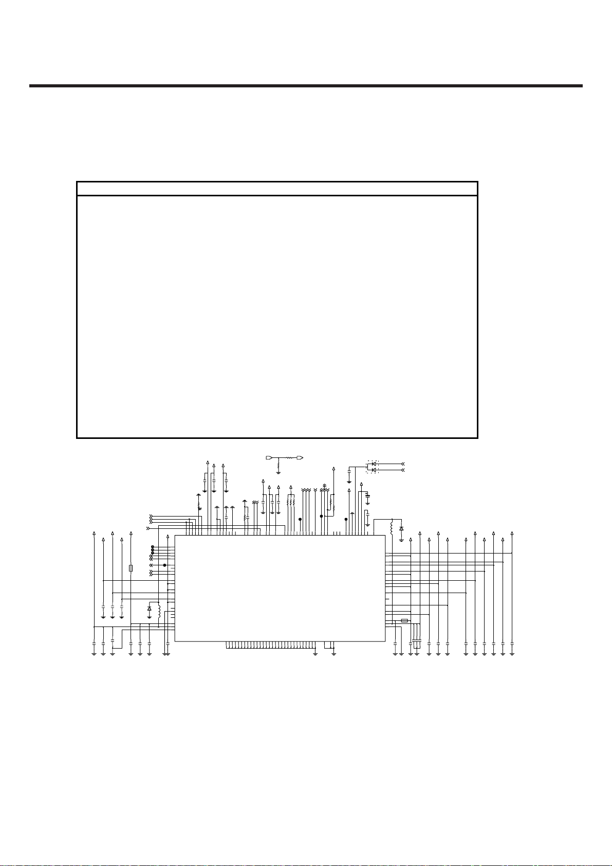
Figure 4 PMIC Circuit
Copyright © 2008 LG Electronics. Inc. All right reserved.
Only for training and service purposes
- 31 -
LGE Internal Use Only
 Loading...