


Page 1
Date: May, 2008 / Issue 1.0
Service Manual
Internal Use Only
Service Manual
KC550
Model : KC550
Page 2

LGE Internal Use Only
Copyright © 2008 LG Electronics. Inc. All right reserved.
Only for training and service purposes
- 3 -
* The information in this manual is subject to change without notice and should not be construed as a
commitment by LGE Inc. Furthermore, LGE Inc. reserves the right, without notice, to make changes to
equipment design as advances in engineering and manufacturing methods warrant.
* This manual provides the information necessary to install, program, operate and maintain the KC550.
REVISED HISTORY
Editor Date Issue Contents of Changes S/W Version
Y.W.YUN 5/26 0.1
Page 3

- 4 -
LGE Internal Use Only
Copyright © 2008 LG Electronics. Inc. All right reserved.
Only for training and service purposes
Page 4

LGE Internal Use Only
Copyright © 2008 LG Electronics. Inc. All right reserved.
Only for training and service purposes
- 5 -
1. INTRODUCTION ...............................7
1.1 Purpose .................................................. 7
1.2 Regulatory Information............................ 7
1.3 ABBREVIATION ..................................... 9
2. GENERAL PERFORMANCE ..........11
2.1 H/W Features.........................................11
2.2 Technical specification...........................12
3. TECHNICAL BRIEF ........................19
3.1 KC550 Component Block diagram.........19
3.2 Main Chip Introduction ...........................20
3.3 Baseband Part Introduction ...................22
3.4 Power Management Unit .......................38
3.5 Power ON/OFF ......................................43
3.6 SIM interface..........................................47
3.7 Memory ..................................................48
3.8 LCD Display ...........................................50
3.9 Keypad Switching & Scanning ...............53
3.10 Keypad back-light illumination .............54
3.11 LCD back-light illumination ..................55
3.12 JTAG interface connector ....................57
3.13 Audio....................................................58
3.14 USB charging circuit ............................62
3.15 BLUETOOTH .......................................63
3.16 FM Radio..............................................66
3.17 Micro SD external memory card slot....67
3.18 18pin Multi Media Interface
connector .............................................69
4. RF circuit technical brief ...............71
4.1 General Description ...............................71
4.2 Receiver part..........................................73
4.3 Transmitter part......................................74
4.4 RF synthesizer .......................................75
4.5 DCXO.....................................................76
4.6 Front End Module control.......................76
4.7 Power Amplifier Module .........................77
4.8 Mode Selection ......................................78
5. PCB layout......................................79
5.1 Main PCB component placement ..........79
6. Trouble shooting............................84
6.1 Trouble shooting test setup....................84
6.2 Power on Trouble...................................85
6.3 Charging trouble ....................................88
6.4 LCD display trouble................................90
6.5 Camera Trouble .....................................93
6.6 Receiver & Speaker trouble ...................95
6.7 Microphone trouble ................................97
6.8 Ear-MIc Jack Detection trouble..............98
6.9 Vibrator trouble ......................................99
6.10 Keypad back light trouble...................100
6.11 SIM & uSD trouble .............................103
6.12 RF Troubleshooting ...........................106
6.13 RF Receiver path Troubleshooting ....110
6.14 RF Transmitter path Troubleshooting 113
7. Download & S/W upgrade...............118
7.1 Download program user guide.............118
7.2 Multi-Download Program Setting .........119
8. CIRCUIT DIAGRAM ......................121
9. BGM PIN MAP...............................131
10. PCB LAYOUT..............................137
11. RF Calibration.............................145
11.1 Test Equipment Setup .......................145
11.2 Calibration Step .................................145
12. Stand-alone Test ........................151
12.1 Test Program Setting .........................151
12.2 Tx Test ...............................................153
12.3 Rx Test...............................................154
13. ENGINEERING MODE ................155
14. EXPLODED VIEW &
REPLACEMENT PART LIST ......157
14.1 Exploded View ...................................157
14.2 Replacement Parts ............................159
14.3 Accessory ..........................................182
Table Of Contents
Page 5

- 6 -
LGE Internal Use Only
Copyright © 2008 LG Electronics. Inc. All right reserved.
Only for training and service purposes
Page 6

- 7 -
1. INTRODUCTION
1.1 Purpose
This manual provides the information necessary to repair, calibration, description and download the
features of the KC550.
1.2 Regulatory Information
A. Security
Toll fraud, the unauthorized use of telecommunications system by an unauthorized part (for example,
persons other than your company’s employees, agents, subcontractors, or person working on your
company’s behalf) can result in substantial additional charges you°Øre your telecommunications
services. System users are responsible for the security of own system.
There are may be risks of toll fraud associated with your telecommunications system. System users
are responsible for programming and configuring the equipment to prevent unauthorized use. LGE
does not warrant that this product is immune from the above case but will prevent unauthorized use of
common-carrier telecommunication service of facilities accessed through or connected to it. LGE will
not be responsible for any charges that result from such unauthorized use.
B. Incidence of Harm
If a telephone company determines that the equipment provided to customer is faulty and possibly
causing harm or interruption in service to the telephone network, it should disconnect telephone
service until repair can be done. A telephone company may temporarily disconnect service as long as
repair is not done.
C. Changes in Service
A local telephone company may make changes in its communications facilities or procedure. If these
changes could reasonably be expected to affect the use of the KC550 or compatibility with the network,
the telephone company is required to give advanced written notice to the user, allowing the user to take
appropriate steps to maintain telephone service.
D. Maintenance Limitations
Maintenance limitations on the KC550 must be performed only at the LGE or its authorized agents.
The user may not make any changes and/or repairs expect as specifically noted in this manual.
Therefore, note that unauthorized alternations or repair may affect the regulatory status of the system
and may void any remaining warranty.
1. INTRODUCTION
LGE Internal Use Only
Copyright © 2008 LG Electronics. Inc. All right reserved.
Only for training and service purposes
Page 7

- 8 -
1. INTRODUCTION
E. Notice of Radiated Emissions
The KC550 complies with rules regarding radiation and radio frequency emission as defined by local
regulatory agencies. In accordance with these agencies, you may be required to provide information
such as the following to the end user.
F. Pictures
The pictures in this manual are for illustrative purposes only; your actual hardware may look slightly
different.
G. Interference and Attenuation
An KC550 may interfere with sensitive laboratory equipment, medical equipment, etc. Interference
from unsuppressed engines or electric motors may cause problems.
H. Electrostatic Sensitive Devices
ATTENTION
Boards, which contains Electrostatic Sensitive Device(ESD), are indicated by the sign.
Following information is ESD handling: Service personnel should ground themselves by using a wrist
strap when exchange system boards.
When repairs are made to a system board, they should spread the floor with anti-static mat which is
also grounded. Use a suitable, grounded soldering iron. Keep sensitive parts in these protective
packages until these are used. When returning system boards or parts such as EEPROM to the
factory, use the protective package as described.
LGE Internal Use Only
Copyright © 2008 LG Electronics. Inc. All right reserved.
Only for training and service purposes
Page 8

- 9 -
1. INTRODUCTION
1.3 ABBREVIATION
For the purposes of this manual, following abbreviations apply:
LGE Internal Use Only
Copyright © 2008 LG Electronics. Inc. All right reserved.
Only for training and service purposes
APC Automatic Power Control
BB Baseband
BER Bit Error Ratio
CC-CV Constant Current - Constant Voltage
CLA Cigar Lighter Adapter
DAC Digital to Analog Converter
DCS Digital Communication System
dBm dB relative to 1 milli-watt
DSP Digital Signal Processing
EEPROM Electrical Erasable Programmable Read-Only Memory
EGPRS Enhanced General Packet Radio Service
EL Electroluminescence
ESD Electrostatic Discharge
FPCB Flexible Printed Circuit Board
GMSK Gaussian Minimum Shift Keying
GPIB General Purpose Interface Bus
GPRS General Packet Radio Service
GSM Global System for Mobile Communications
IPUI International Portable User Identity
IF Intermediate Frequency
LCD Liquid Crystal Display
LDO Low Drop Output
LED Light Emitting Diode
Page 9
LGE Internal Use Only
Copyright © 2008 LG Electronics. Inc. All right reserved.
Only for training and service purposes
1. INTRODUCTION
- 10 -
LGE LG Electronics
OPLL Offset Phase Locked Loop
PAM Power Amplifier Module
PCB Printed Circuit Board
PGA Programmable Gain Amplifier
PLL Phase Locked Loop
PSTN Public Switched Telephone Network
RF Radio Frequency
RLR Receiving Loudness Rating
RMS Root Mean Square
RTC Real Time Clock
SAW Surface Acoustic Wave
SIM Subscriber Identity Module
SLR Sending Loudness Rating
SRAM Static Random Access Memory
STMR Side Tone Masking Rating
TA Travel Adapter
TDD Time Division Duplex
TDMA Time Division Multiple Access
UART Universal Asynchronous Receiver/Transmitter
VCO Voltage Controlled Oscillator
VCTCXO Voltage Control Temperature Compensated Crystal Oscillator
WAP Wireless Application Protocol
8PSK 8 Phase Shift Keying
Page 10
- 11 -
2. GENERAL PERFORMANCE
2.1 H/W Feature
2. GENERAL PERFORMANCE
LGE Internal Use Only
Copyright © 2008 LG Electronics. Inc. All right reserved.
Only for training and service purposes
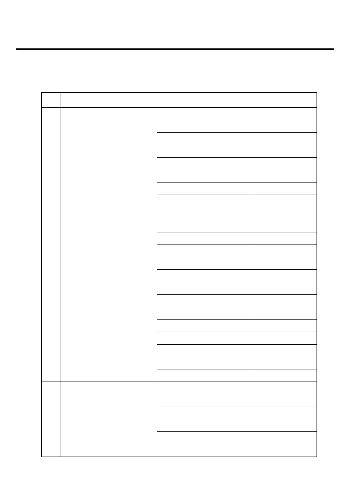
Item Feature Comment
Standard Battery Li-ion, 900mAh
AVG TCVR Current 260mA typ @PL5
Standby Current 2 mA typ @PP9
Talk time 6 hours (GSM TX Level 10)
Standby time Over 450 hours (Paging Period:9, RSSI: -85dBm)
Charging time Under 3 hours
RX Sensitivity EGSM : -105dBm↓ , DCS/PCS : -105dBm↓
TX output power EGSM : 33dBm (@PL 5)
DCS/PCS: 30dBm (@PL 0)
GPRS compatibility Class 12
SIM card type 3V Small
Display 240 x 320 pixels, 2.4 inch QVGA, 262K color, TFT
Status Indicator Soft icons, 0 ~ 9, #, *, Scroll, Send, End/PWR,
Clear AF/Camera double action, Volume Up,
Volume Down
ANT Built in antenna
EAR Phone Jack 18pin multi port Headset jack (W/O remote controller)
PC Synchronization Yes
Speech coding HR/EFR/FR/AMR
Data and Fax Yes
Vibrator Yes
Buzzer No
Voice Recoding Yes
C-Mic Yes
Receiver Yes
Travel Adapter Yes
Options Bluetooth hands-free kit, Data Kit
Page 11
- 12 -
2. GENERAL PERFORMANCE
2.2 Technical specification
LGE Internal Use Only
Copyright © 2008 LG Electronics. Inc. All right reserved.
Only for training and service purposes
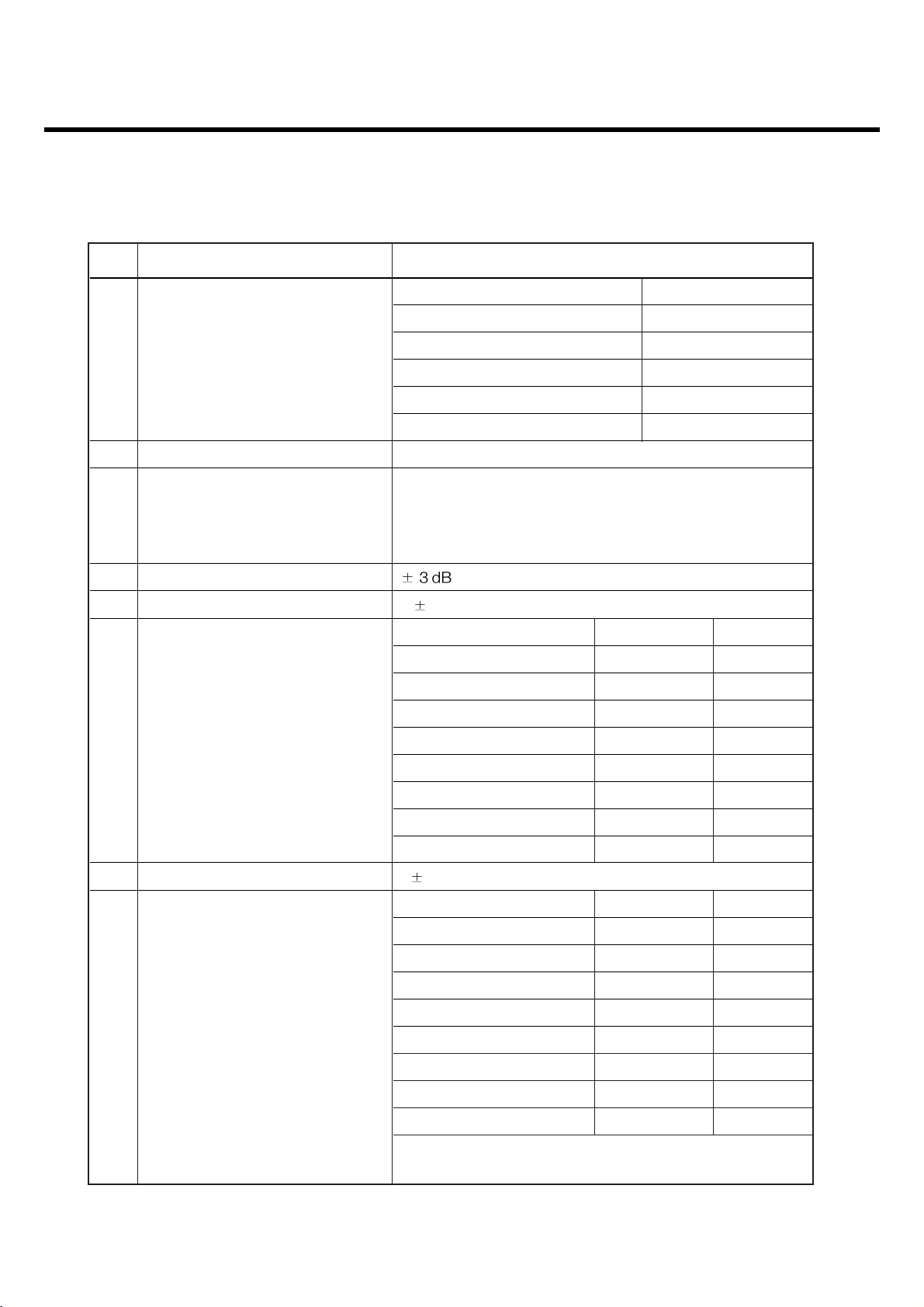
Item Description Specification
1Frequency Band EGSM
TX: 890 + 0.2 x n MHz
RX: 935 + 0.2 x n MHz ( n = 1 ~ 124 )
TX: 890 + 0.2 x (n-1024) MHz
RX: 935 + 0.2 x (n-1024) MHz ( n = 975 ~ 1023 )
DCS1800
TX: 1710 + ( n-511 ) x 0.2 MHz (n = 512 ~ 885)
RX: TX + 95 MHz
PCS1900
TX: 1850.2 + ( n-512 ) x 0.2 MHz (n = 512 ~ 810)
RX: TX + 80MHz
2 Phase Error RMS < 5 degrees ,
Peak < 20 degrees
3 Frequency Error < 0.1ppm
4 Power Level EGSM
Level Power Toler. Level Power Toler.
5 33 dBm 2dB 13 17 dBm 3dB
6 31 dBm 3dB 14 15 dBm 3dB
7 29 dBm 3dB 15 13 dBm 3dB
8 27 dBm 3dB 16 11 dBm 5dB
9 25 dBm 3dB 17 9 dBm 5dB
10 23 dBm 3dB 18 7 dBm 5dB
11 21 dBm 3dB 19 5 dBm 5dB
12 19 dBm 3dB
DCS1800/PCS1900
Level Power Toler. Level Power Toler.
0 30 dBm 2dB 8 14 dBm 3dB
1 28 dBm 3dB 9 12 dBm 4dB
2 26 dBm 3dB 10 10 dBm 4dB
3 24 dBm 3dB 11 8 dBm 4dB
4 22 dBm 3dB 12 6 dBm 4dB
5 20 dBm 3dB 13 4 dBm 4dB
6 18 dBm 3dB 14 2 dBm 5dB
7 16 dBm 3dB 15 0 dBm 5dB
Page 12
- 13 -
2. GENERAL PERFORMANCE
LGE Internal Use Only
Copyright © 2008 LG Electronics. Inc. All right reserved.
Only for training and service purposes
Item Description Specification
5 Output RF Spectrum EGSM
(due to modulation) Offset from Carrier (kHz). Max. dBc
100 +0.5
200 -30
250 -33
400 -60
600 ~ 1,200 -60
1,200 ~ 1,800 -60
1,800 ~ 3,000 -63
3,000 ~ 6,000 -65
6,000 -71
DCS1800/PCS1900
Offset from Carrier (kHz). Max. dBc
100 +0.5
200 -30
250 -33
400 -60
600 ~ 1,200 -60
1,200 ~ 1,800 -60
1,800 ~ 3,000 -65
3,000 ~ 6,000 -65
6,000 -73
6 Output RF Spectrum EGSM
(due to switching transient) Offset from Carrier (kHz) Max. (dBm)
400 -19
600 -21
1,200 -21
1,800 -24
Page 13
- 14 -
2. GENERAL PERFORMANCE
LGE Internal Use Only
Copyright © 2008 LG Electronics. Inc. All right reserved.
Only for training and service purposes
Item Description Specification
6 Output RF Spectrum DCS1800/PCS1900
(due to switching transient) Offset from Carrier (kHz). Max. (dBm)
400 -22
600 -24
1,200 -24
1,800 -27
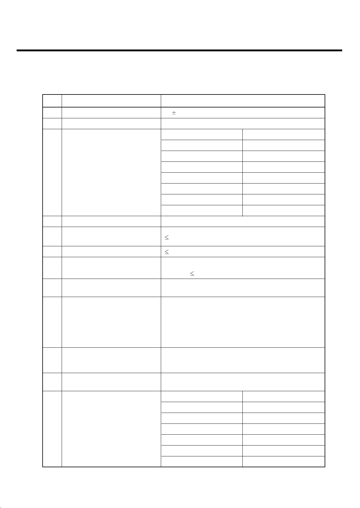
7 Spurious Emissions Conduction, Emission Status
8 Bit Error Ratio EGSM
BER (Class II) < 2.439% @-102dBm
DCS1800/PCS1900
BER (Class II) < 2.439% @-100dBm
9 Rx Level Report accuracy
10 SLR 8 3 dB
11 Sending Response Frequency (Hz) Max.(dB) Min.(dB)
100 -12 -
200 0 -
300 0 -12
1,000 0 -6
2,000 4 -6
3,000 4 -6
3,400 4 -9
4,000 0 -
12 RLR 2 3 dB
13 Receiving Response Frequency (Hz) Max.(dB) Min.(dB)
100 -12 -
200 0 -
300 2 -7
500
*
-5
1,000 0 -5
3,000 2 -5
3,400 2 -10
4,000 2
*
Mean that Adopt a straight line in between 300 Hz
and 1,000 Hz to be Max. level in the range.
Page 14
- 15 -
2. GENERAL PERFORMANCE
LGE Internal Use Only
Copyright © 2008 LG Electronics. Inc. All right reserved.
Only for training and service purposes
Item Description Specification
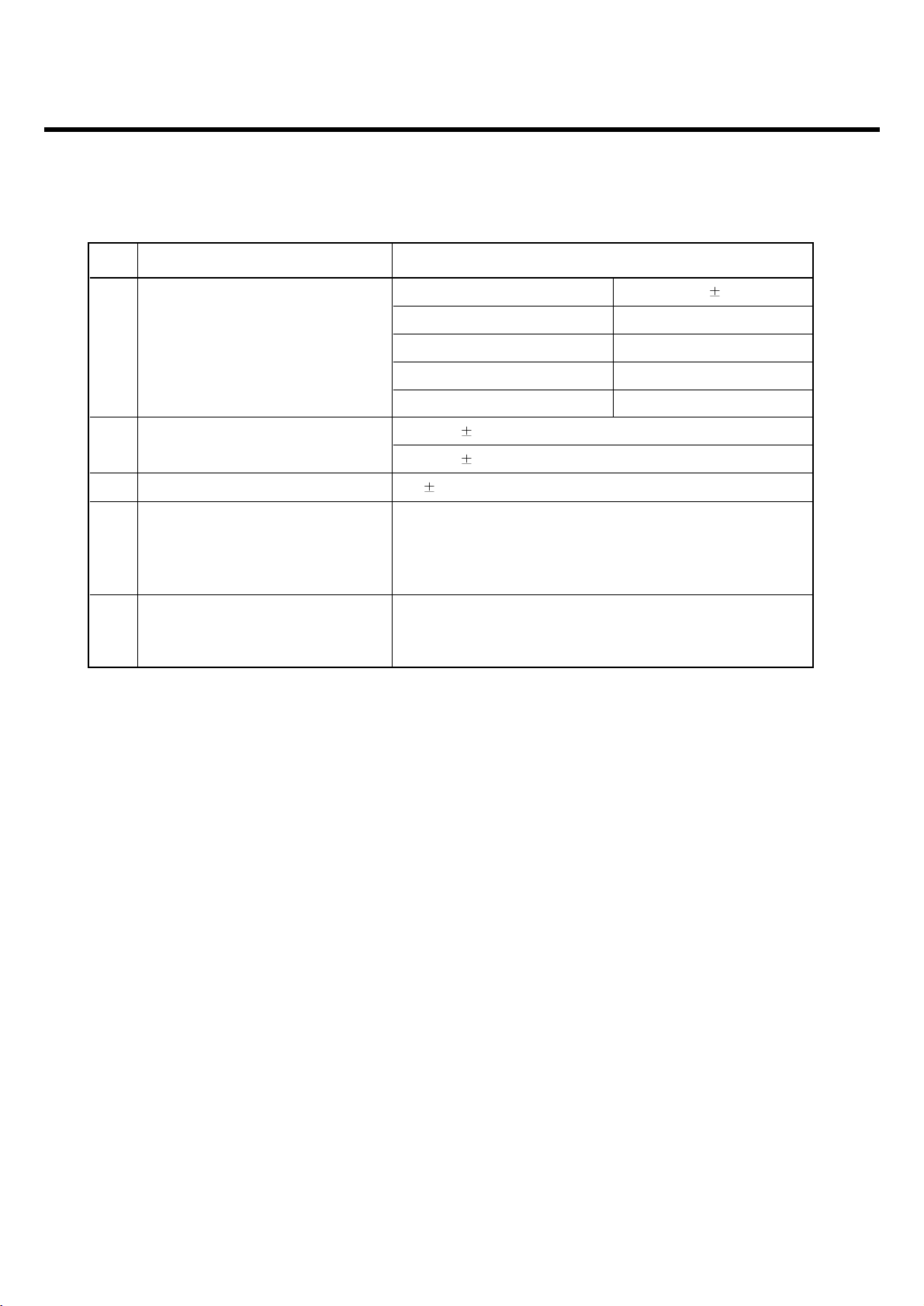
14 STMR 13 5 dB
15 Stability Margin > 6 dB
16 Distortion dB to ARL (dB) Level Ratio (dB)
-35 17.5
-30 22.5
-20 30.7
-10 33.3
0 33.7
7 31.7
10 25.5
17 Side Tone Distortion Three stage distortion < 10%
18
System frequency
2.5ppm
(26 MHz) tolerance
19 32.768KHz tolerance 30ppm
20 Power consumption Standby
- Normal 2 mA(@PP9)
21 Talk Time EGSM/Lvl 7 (Battery Capacity 900mA):180min
EGSM/Lvl12(Battery Capacity 900mA): 320min
22 Standby Time Under conditions, at least 300 hours:
1. Brand new and full 900mAh battery
2. Full charge, no receive/send and keep GSM in idle mode.
3. Broadcast set off.
4. Signal strength display set at 3 level above.
5. Backlight of phone set off.
23 Ringer Volume At least 65 dB under below conditions:
1. Ringer set as ringer.
2. Test distance set as 50 cm
24 Charge Current Fast Charge : < 450 mA
Slow Charge: < 200 mA
25 Antenna Display Antenna Bar Number Power
7 >-92 dBm ~
7 → 5 -97dBm ~ -93dBm
5 → 4 -100dBm ~ -98dBm
4 → 2 -103dBm ~ -101dBm
2 → 1 -105dBm ~ -104dBm
1 → 0< -106 dBm
Page 15
LGE Internal Use Only
Copyright © 2008 LG Electronics. Inc. All right reserved.
Only for training and service purposes
2. GENERAL PERFORMANCE
- 16 -
Item Description Specification
26 Battery Indicator Battery Bar Number Voltage( 0.05V)
3 3.76V~4.2V
2 3.68V~3.75V
1 3.55V~3.65V
0 3.41V~
27 Low Voltage Warning 3.58V ↓ 0.05V (Call)
3.51V ↓ 0.05V (Standby)
28 Forced shut down Voltage 3.3 0.05 V
29 Battery Type Li-ion Battery or Li-Polymer Battery
Standard Voltage = 3.7 V
Battery full charge voltage = 4.2 V
Capacity: 900mAh
31 Travel Charger Switching-mode charger
Input: 100 ~ 240 V, 50/60Hz
Out put: 5.1, 0.7A
Page 16
LGE Internal Use Only
Copyright © 2008 LG Electronics. Inc. All right reserved.
Only for training and service purposes
2. GENERAL PERFORMANCE
- 17 -
* EDGE RF Specification (Option: is not serviced for “EDGE mode”)
Item Description Specification
1 RMS EVM 9%
2 Peak EVM 30%
395thPercentile EVM 15%
4Origin Offset Suppression ≥ 30dB
5 Power Level EGSM
Level Power Toler. Level Power Toler.
5 27dBm 3dB 13 17dBm 3dB
6 27dBm 3dB 14 15dBm 3dB
7 27dBm 3dB 15 13dBm 3dB
8 27dBm 3dB 16 11dBm 5dB
9 25dBm 3dB 17 9dBm 5dB
10 23dBm 3dB 18 7dBm 5dB
11 21dBm 3dB 19 5dBm 5dB
12 19dBm 3dB
DCS1800, PCS1900
Level Power Toler. Level Power Toler.
0 26dBm 3dB 8 14dBm 3dB
1 26dBm 3dB 9 12dBm 4dB
2 26dBm 3dB 10 10dBm 4dB
3 24dBm 3dB 11 8dBm 4dB
4 22dBm 3dB 12 6dBm 4dB
5 20dBm 3dB 13 4dBm 4dB
6 18dBm 3dB 14 2dBm 5dB
7 16dBm 3dB 15 0dBm 5dB
6 Output RF Spectrum EGSM
(due to modulation) Offset from carrier(kHz) Max. dBc
100 +0.5
200 -30
250 -33
400 -54
600 ~ <1,200 -60
1,200 ~ <1,800 -60
1,800 ~ <3,000 -63
3,000 ~ <6,000 -65
6,000 -71
Page 17
LGE Internal Use Only
Copyright © 2008 LG Electronics. Inc. All right reserved.
Only for training and service purposes
2. GENERAL PERFORMANCE
- 18 -
Item Description Specification
6 Output RF Spectrum DCS1800, PCS1900
(due to modulation) Offset from carrier(kHz) Max. dBc
100 +0.5
200 -30
250 -33
400 -54
600 ~ <1,200 -60
1,200 ~ <1,800 -60
1,800 ~ <3,000 -63
3,000 ~ <6,000 -65
6,000 -71
7 Output RF Spectrum EGSM
(due to switching transient) Offset from carrier(kHz) Max. dBm
400 -23
600 -26
1,200 -27
1,800 --30
DCS1800, PCS1900
Offset from carrier(kHz) Max. dBm
400 -23
600 -26
1,200 -27
1,800 -30
Page 18
LGE Internal Use Only
Copyright © 2008 LG Electronics. Inc. All right reserved.
Only for training and service purposes
3. TECHNICAL BRIEF
- 19 -
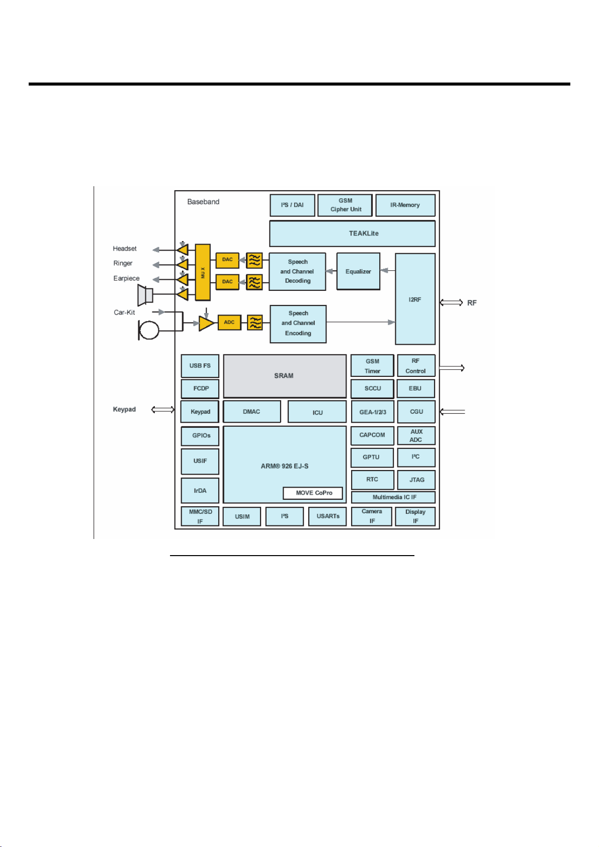
3.1 KC550 Component Block diagram
KC550 is composed with 5 different PCB part such as main PCB, Key PCB, Key FPCB, LCD FPCB
and Flash FPCB/
The functional component arrangement is mentioned below diagram.
3. TECHNICAL BRIEF
Figure 1 KC550 Functional block diagram
Flash LED
PWF4
5M Pxl, AF
2.4î QVGA TFT
2.4î QVGA TFT
(240x320)
(240x320)
KEYPAD
Acceleration
Sensor
: Signal , Control Connection
: RF Connection
: Power Connection
: Mechanical Connection
MIPI I/F
LCD 16bit
I/F
DC/DC
Converter
Charge
Pump
BD6095
LCD B/L
Camera LDO
(1.8V, 2.8V)
MMIC/ISP
M180
Audio Codec+AMP
WM8990
16pi, 3.4t
SPK
LP3907
1.2V, 1.8V,
MMIC 16bit I/F
Radio TX
signal
512Mb SDRAM)
Headset
antenna
PMIC
2.6V
A/
D/
18
16
Memory
(1Gb NAND +
BT
BT/FM radio
BLUCORE5-FM
SIM
UART
I2S
BB+RF
PMB8888
D/
4
Micro SD
SIM Card
Socket
26MHz
RX IQ
TX IQ
RF Ctrl
Backup
Battery
Charging
VUSB
ISL9221
Battery
900mAh
PAM
TQM7M5005
Radio RX
signal
antenna
FEM
LSHS-C085FB
18pin
I/O
Main
RCV
Motor
Stereo
headset
TA
USB cable
Page 19
- 20 -
3. TECHNICAL BRIEF
3.2 Main Chip Introduction
3.2.1 General Description
world’s first single-chip solution for feature-rich mobile phones. The EDGE-capable device combines
alldigital and analog functions of the baseband, a quad-band RF transceiver, and the power
management circuitry into a single chip. With an option for memory stacking (“Package on Package”,
JEDEC compliant) the key functions of a mobile phone are now combined into a single device,
providing all the benefits that come from a maximum level of integration. Full software re-use from the
proven Infineon EDGE platform, MP-ELite, enables fast time-to-market using a comprehensive
development kit available to all customers today.
set of multimedia applications such as:
LGE Internal Use Only
Copyright © 2008 LG Electronics. Inc. All right reserved.
Only for training and service purposes
Page 20

- 21 -
3. TECHNICAL BRIEF
• Still picture imaging up to 2 MPixel
• MPEG4 video encode/decode
• Video streaming
• MP3 playback
LGE Internal Use Only
Copyright © 2008 LG Electronics. Inc. All right reserved.
Only for training and service purposes
Page 21
- 22 -
3. TECHNICAL BRIEF
3.3 Baseband Part Introduction
3.3.1 Block Description
Connectivity
applications:
• USB 2.0 Full Speed (12 Mbps)
• IrDA Controller
Supports Infrared SIR Mode Transceivers
• RS-232 over a 16C550 compliant UART
• MMC/SD Memory Card Interface
- Low Voltage Capable
- SDIO expandable (using external components)
LGE Internal Use Only
Copyright © 2008 LG Electronics. Inc. All right reserved.
Only for training and service purposes
Page 22

- 23 -
3. TECHNICAL BRIEF
• Ready to connect to the Infineon’s Bluemoon Family Bluetooth Transceivers
- HCI (H5) optimized USIF (Universal Serial Interface)
- Dedicated PCM-style digital audio interface (I2S)
- Dedicated power supply
• Microcontroller-Like Extension Interface
For multimedia companions (for example, complex display/camera modules or graphic accelerators)
• External Memory Interface
Supporting:
- SDRAM
- Cellular RAM
- Burst Flash
- SRAM
- NAND flashes (error correction capability in HW)
• User Interface (Keypad)
Supporting up to 74 keys with multiple key-press capability
• SIM Card interface (USIM)
ISO 7816 compatible
• Analogue Measurement Unit
For various general purpose measurements such as battery voltage, battery, VCXO and
environmental temperature, battery technology, transmission power, offset, on-chip temperature, etc.
Security
• Secure Boot and Flash Update
• SHA1 HW acceleration
• Secure Debug
• 128-bit customer defined efuse key
• Anti-intrusion logic.
Audio
Besides the telephony voice CODECs supplied by the Firmware running on the TEAKLite® DSP core,
the ARM926 core enables running high-quality audio CODECs such as MPEG-1/2 Layer-3 Decode
(MP3), AAC+ or AAC++. Audio streaming is supported according to the 3GPP PSS Release 4
standard.
The output of audio and voice codecs can be mixed and routed to the integrated Hi-Fi Stereo
voiceband supporting CD-Quality. Alternatively, the audio can also be sinked to a mono loudspeaker
using the integrated hands-free amplifier.
LGE Internal Use Only
Copyright © 2008 LG Electronics. Inc. All right reserved.
Only for training and service purposes
Page 23

- 24 -
3. TECHNICAL BRIEF
Video and Imaging
interface and a display module over a microcontroller-like parallel or serial interface. Furthermore,
ARM’s MOVE coprocessor is integrated to accelerate video encoding algorithms (for example, H.263
or MPEG-4). This fulfills basic multimedia requirements and allows connecting commodity cameras
and displays without the need of an additional multimedia IC. The computational power for encoding
and decoding still pictures (JPEG) and video sequences (H.263 or MPEG-4) is provided by the
integrated ARM926 core.
Over-the-air interface JPEG pictures and H.263 or MPEG-4 videos can be sent or received as MMS by
means of (E)GPRS.
Supported "still pictures" multimedia scenarios are:
• View Finding for a Picture Snapshot: Captured frames are transferred from the camera IF to the
display IF at up to15 fps (depending on the camera used) in QCIF resolution (depending on the
display used). Downscaling and color conversion is done by the camera and display interface logic.
Therefore, view finding for a snapshot is possible without burdening the CPU. However, picture
rotation and/or overlay are performed by SW if required.
• Shooting: The captured picture, with up to 1.31 MPixel resolution (SXGA 1280 x 1024), is
transferred within 1/15 sec to external memory.1) Then, JPEG compression is done by SW, while the
viewfinder is frozen so that the user can immediately see the snapshot on the display.
• Photo Flash: Under low light conditions usually a photo flash is required. To activate the flash at the
right time, a general purpose timer unit (GTPU) can be used that is triggered by the frame
synchronization signal (VSYNC) from the camera interface.
• Processing: JPEG thumbnail generation, picture overlay, picture rotation and other picture
processing tasks are performed by SW.
• Viewing: A JPEG picture is decoded, down-scaled and format converted by SW and then transferred
to the display interface. JPEG thumbnails can also be transferred directly to the display interface after
decoding by SW without additional downscaling.
• Storage: JPEG pictures can be stored on an MMC/SD card, a Flash or a PC.
• Sending/Receiving: JPEG thumbnails can be sent/received as MMS (E-GPRS). Full resolution
JPEG pictures can be sent/received as e-mail or downloaded from the internet.
Supported "video sequence" multimedia scenarios:
• Record Video Sequences: Captured frames in QCIF resolution are transferred to internal memory
at 15 fps. H.263 or MPEG-4 encoding is performed on-the-fly by SW with the support of the MOVE
coprocessor.
The audio recording is performed on the DSP (GSM AMR CODEC). Multiplexing of audio and video
streams is performed by the ARM.
LGE Internal Use Only
Copyright © 2008 LG Electronics. Inc. All right reserved.
Only for training and service purposes
Page 24

- 25 -
3. TECHNICAL BRIEF
• View Finding during Video Encoding: During video recording the user needs to see what is being
recorded. Therefore, the captured frames are not only encoded but also transferred to the display
interface. If only every second frame from the camera is used for encoding, viewfinding is possible
without burdening the CPU. However, if each frame from the camera has to be encoded, due to low
camera frame rate, the YCbCr4:2:2 to YCbCr4:4:4 color conversion and further downscaling is
performed by SW.
Picture rotation and overlay has to be done in SW in any case.
• Storage: Compressed H.263 or MPEG-4 videos can be stored on an MMC/SD, a Flash or a PC.
• Viewing: De-multiplexing of audio and video streams is performed by the ARM. The H.263 or
MPEG-4 decoding is also done by SW on the ARM and then the frames are transferred to the display
interface.
Audio decoding (GSM-AMR) is done on the DSP.
The audio/video synchronization is done by time stamp feedback from the DSP to the ARM.
• Sending/Receiving: H.263 or MPEG-4 videos can be sent/received as MMS (E-GPRS), as e-mail or
downloaded from the internet.
Higher Multimedia Performance
If higher multimedia performance is required, an external multimedia IC can be connected to S-
interface pins are used in a multiplex mode to connect an external multimedia IC to the S-
multimedia IC, which contains functions (in HW and/or SW) to process still images and video data.
This configuration is intended for higher-end graphics features (for example, high quality video
streaming, video conferencing, hardware-assisted 2D/3D graphics functions, etc.).
LGE Internal Use Only
Copyright © 2008 LG Electronics. Inc. All right reserved.
Only for training and service purposes
Page 25
- 26 -
3. TECHNICAL BRIEF
3.3.2 External Devices connected to memory interface
Table 1 Memory interface
3.3.3 RF Interface
RF ICs Periodically each TDMA frame.
Table 2. RF Interface Spec
.
LGE Internal Use Only
Copyright © 2008 LG Electronics. Inc. All right reserved.
Only for training and service purposes
Device Name Maker Remark
FLASH K5D1G12ACE-D075 SAMSUNG 1G(128Mx8) NAND
SDRAM K5D1G12ACE-D075 SAMSUNG 512M(32Mx16) SDRAM
LCD TX08D13VM0AAA TMD 16bit access 2times transmission
Multimedia IC 215-0638018 AMD Multimedia processing
T_OUT
Resource Interconnection Description
PABS PA_BAND TX RF band select
PAMODE PA_MODE PAM Mode select
FE1 VC1 FEM control
FE2 VC2 FEM control
PAEN PA_EN PAM Power on
VRAMP TX_RAMP APC
Page 26
- 27 -
3. TECHNICAL BRIEF
3.3.4 USART Interface
KC550 have a UART Driver as follow :
- USART1 : Hardware Flow Control / SW upgrade / Calibration
Table 3. USIF Interface Spec.
3.3.5 ADC channel
BBP ADC block is composed of 7 external ADC channel. This block operates charging process and
other related process by reading battery voltage and other analog values.
LGE Internal Use Only
Copyright © 2008 LG Electronics. Inc. All right reserved.
Only for training and service purposes
USART_0(USART1)
Resource Name Remark
USART0_TXD UART_TX Transmit Data
USART0_RXD UART_RX Receive Data
USART0_CTS ACCEL_INT Interrupt
USART0_RTS MMC_DETECT GPIO
DSPOUT_0 JACK_DETECT Interrupt
ADC channel
Resource Interconnection Description
M0 BATT_ID Battery IC check
M1 RF_TEMP RF block temperature measure
M2 N.C.
M8 VSUPPLY Battery supply voltage measure
M9 N.C.
M10 REMOTE_ADC Remote control key detect
Page 27
3.3.6 GPIO map
Over a hundred allowable resources, KC550 is using as follows except dedicated to SIM and Memory.
KC550 GPIO(General Purpose Input/Output) Map, describing application, I/O state, and enable level,
is shown in below table.
- 28 -
3. TECHNICAL BRIEF
LGE Internal Use Only
Copyright © 2008 LG Electronics. Inc. All right reserved.
Only for training and service purposes
Port Function Net Name Description
#Keypad
KP_IN0 NONE
KP_IN1 KP_IN(1)
KP_IN2 KP_IN(2)
KP_IN3 KP_IN(3)
KP_IN4 KP_IN(4)
KP_IN5 KP_IN(5)
KP_IN6 KP_IN(6)
KP_OUT0 KP_OUT(0)
KP_OUT1 KP_OUT(1)
KP_OUT2 KP_OUT(2)
KP_OUT3 KP_OUT(3)
#USART0
USART0_RXD UART_RX
USART0_TXD UART_TX
USART0_RTS_N MMC_DETECT
USART0_CTS_N ACCEL_INT
DSPOUT0 JACK_DETECT
#USB
USB_DPLUS USB_DP
USB_DMINUS USB_DM
#CIF:Camera Interface
CIF_D0 MM_AD0
CIF_D1 MM_AD1
CIF_D2 MM_AD2
Page 28
- 29 -
3. TECHNICAL BRIEF
LGE Internal Use Only
Copyright © 2008 LG Electronics. Inc. All right reserved.
Only for training and service purposes
CIF_D3 MM_AD3
CIF_D4 MM_AD4
CIF_D5 MM_AD5
CIF_D6 MM_AD6
CIF_D7 MM_AD7
CIF_PCLK
CIF_HSYNC MM_WAIT
CIF_VSYNC TP
CLKOUT2 GPO_CTRL1
CIF_PD_GPIO HS_SEL N.A
CIF_RESET_GPIO GPO_CTRL2
#Display_Interface
DIF_D0 MM_AD8
DIF_D1 MM_AD9
DIF_D2 MM_AD10
DIF_D3 MM_AD11
DIF_D4 MM_AD12
DIF_D5 MM_AD13
DIF_D6 MM_AD14
DIF_D7 MM_AD15
DIF_CS1 MM_CS0
DIF_CS2 REMOTE_INT
DIF_CD MM_A16
DIF_WR MM_WR
DIF_RD MM_RD
DIF_HD MM_INT
DIF_VD BT_INT
DIF_RESET1_GPIO HOOK_DETECT
#I2C
I2C_SCL I2C_SCL
I2C_SDA I2C_SDA
PM_INT NONE
Page 29
- 30 -
3. TECHNICAL BRIEF
LGE Internal Use Only
Copyright © 2008 LG Electronics. Inc. All right reserved.
Only for training and service purposes
#Chip Card (USIM1)
CC_IO SIM_IO
CC_CLK SIM_CLK
CC_RST SIM_RST
#MMCI: Multimedia Card IF
MMCI_CMD MMCI_CMD
MMCI_DAT0 MMCI_DAT0
MMCI_CLK MMCI_CLK
#USIF: Universal Serial IF
USIF_TXD_MTSR UART_BT_TX
USIF_RXD_MRST UART_BT_RX
USIF_SCLK BT_VCXO_EN
#I2S1: DAI-PCM
I2S1_CLK0 I2S1_CLK
I2S1_RX I2S1_RX
I2S1_TX I2S1_TX
I2S1_WA0 I2S1_WA0
#MMCI: SD-Extension
MMCI_DAT1 MMCI_DAT1
MMCI_DAT2 MMCI_DAT2
MMCI_DAT3 MMCI_DAT3
#Voiceband: Analog Interface
EP_N SND_L
EP_P SND_R
HS_N EAR_N
EP_CM NA
HS_P EAR_P
MIC1_N MIC_N
MIC1_P MIC_P
MIC2_N HS_MIC_N
MIC2_P HS_MIC_P
VMIC VMIC
Page 30
#Measurement
M0 BAT_ID
M1 RF_TEMP
M2 JACK_TYPE
M7 GND
M8 VBAT
M9 LOAD
M10 REMOTE_ADC
#Bandgap reference: Analog Interface
VREF2 GND
IREF2 GND
#JTAG
TDO TDO
TDI TDI
TMS TMS
TCK TCK
TRST_n TRST_N
RTCK RTCK
#Debug
TRIG_IN TRIG_IN
MON1 MON1
MON2 MON2
#External Bus Interface (EBU)
#FCDP: Flash Controller DMA Port
FCDP_RBN FCDP
#GSM TDMA Timer: GSM Control
T_OUT1 NONE
T_OUT2 NONE
T_OUT3 UART_BT_RTS
T_OUT4 UART_BT_CTS
T_OUT5 FLIP_OPEN
T_OUT6 PA_MODE_2
- 31 -
3. TECHNICAL BRIEF
LGE Internal Use Only
Copyright © 2008 LG Electronics. Inc. All right reserved.
Only for training and service purposes
Page 31

- 32 -
3. TECHNICAL BRIEF
LGE Internal Use Only
Copyright © 2008 LG Electronics. Inc. All right reserved.
Only for training and service purposes
T_OUT7 KP_OUT(4)
T_OUT8 DSR
#Other Functional Pins: Clocks and control
CLKOUT0 LCD_ID
F26M NONE
F32K F32K
OSC32K OSC32K
RESET_N nRESET
VDD_FUSE_FS GND
RTC_OUT NONE
PMU_SCMODE_OUT NONE
VCXO_EN NONE
#Extra I/Os & Interrupt Inputs
DSPIN0 CLK32K
DSPIN1 CHG_EOC
#Digital Power supply
VDD_MAIN VSD1_1V5
VSS_MAIN GND
VDDP_EBU1 VSD2_1V8
VSSP_EBU NONE
VDDP_DIG NONE
VDDP_SIM NONE
VDDP_MMC NONE
VDD_RTC NONE
VSS_RTC NONE
VDD_PLL NONE
VDD_USB NONE
#Analog Power Supply
VAUDIO VAUDIO_2V5
VSS_MS GND
VSS_EP GND
AGND_MS1~2 GND
Page 32

- 33 -
3. TECHNICAL BRIEF
LGE Internal Use Only
Copyright © 2008 LG Electronics. Inc. All right reserved.
Only for training and service purposes
#RF Front-end
TX2 TXHB
TX1 TXLB
RX1 EGSM_RXP
RX1X EGSM_RXN
RX2 GSM900_RXP
RX2X GSM900_RXN
PABIAS NA
PABS PA_BAND
RX3 DCS1800_RXP
VDET TP
PAMODE PA_MODE
RX3X DCS1800_RXN
FE1 VC1
FE2 VC2
PAEN PA_EN
RX4 PCS1900_RXP
VRAMP TX_RAMP
RX4X PCS1900_RXN
#Baseband I/0
FSYS3 26M_OUT
FSYS2 26M_BT
#Reference Oszillator / PLL
REFR NA
XOX 26MHz
XO 26MHz
#Power Supply
VDDTX VRF3_2V85
VDDVCO VRF3_2V85
VDDTRX VRF2_1V5
VDDDIG VRF3_2V85
VDDMS VRF3_2V85
Page 33

- 34 -
3. TECHNICAL BRIEF
LGE Internal Use Only
Copyright © 2008 LG Electronics. Inc. All right reserved.
Only for training and service purposes
VDDXO VRF1_2V85
VDDPLL VRF3_2V85
VDDRX VRF3_2V85
#Ground Balls
VSSRF1 GND
VSSRF2 GND
VSSRF3 GND
VSSRF4 GND
VSSRF5 GND
VSSRF6 GND
VSSRF7 GND
VSSRF8 GND
VSSRF9 GND
VSSRF10 GND
VSSRF11 GND
VSSRF12 GND
VSSRF13 GND
VSSRF14 GND
#Linear Voltage Reulators
VAUDIO VAUDIO_2V5
VBAT_AUDIO VBAT
VSS_AUDIO GND
VLED TP
VAUX VAUX_2V9
VVIB VVIB_2V8
VBAT_LDO1 VBAT
VSS_LDO1 GND
VMMC VMMC
VUSB VUSB_3V1
VBAT_BSW_USB_MMC VBAT
VIO VIO_2V82
VIOb NONE
Page 34

- 35 -
3. TECHNICAL BRIEF
LGE Internal Use Only
Copyright © 2008 LG Electronics. Inc. All right reserved.
Only for training and service purposes
VSIM VSIM_2V8
VBAT_LDO2 VBAT
VSS_LDO2 GND
VPLL VPLL_1V5
VRF2 VRF2_1V5
VDD_RF2PLL VBAT
VRF1 VRF1_2V85
VRF3 VRF3_2V85
VBAT_RF13 VBAT
VSS_LDO3 GND
#Charger and RTC
CH_SOURCE GND
CH_GATE NA
SENSE_IN1 VBAT
SENSE_IN2 VBAT
VDD_REF GND
VDDCHARGE VCHG, VBUS_USB
VSS_CHARGER NONE
CHARGE_UC / SCAN_IN1 VRTC_2V0
VRTC NONE
#Reference
IREF1 GND
A_GND GND
VREF1
#LED's
BL1_PWM / VSENSE1 TP
BL2_PWM TP
BL3_PWM TP
FLASH_ON NONE
TXONPA NONE
VSS_FLASH GND
FLASH_SINK KEY_BL
Page 35

- 36 -
3. TECHNICAL BRIEF
LGE Internal Use Only
Copyright © 2008 LG Electronics. Inc. All right reserved.
Only for training and service purposes
#Step Down Converter 1 (SD1)
VBAT_SD1 VBAT
VSD1 VSD1_1V5
SD1_FB VSD1_1V5
SD2_SD1_SUBST GND
VSS_SD1 GND
SD1_FBL GND
VDDANA_SW NONE
VSSANA_SW NONE
#Step Down Converter 2 (SD2)
VBAT_SD2 VBAT
VSD2 VSD2_1V8
SD2_FB VSD2_1V8
SD2_FBL GND
VSS_SD2 GND
SD2_SD1_SUBST GND
#Step Up Converter (SU1)
SU_GATE NA
SU_GND GND
SU_FB NA
SU_ISENSE NA
VBAT_SU NA
VSS_SU GND
#Control Logic
LPBCL_ECHO NA
WDOG / SCAN_IN2 NONE
ON_OFF / SCAN_RESET PWRON
ON_OFF2 / SCAN_CLK NONE
VSS_DIG NONE
ON_OFF_OUT NONE
RESET2_N / VSENSE2 NA
PO_RESET_N / SCAN_OUT2 PO_RESET
Page 36

- 37 -
3. TECHNICAL BRIEF
LGE Internal Use Only
Copyright © 2008 LG Electronics. Inc. All right reserved.
Only for training and service purposes
SLEEP_N / SCAN_ENABLE NONE
SCANMODE NONE
I2C_INT / SCAN_OUT1 NONE
I2C_CLK NONE
I2C_DAT NONE
#Audio Loudspeaker Amplifier
VBAT_MONO NA
VSS_MONO NA
MONO_OUTP NA
MONO_OUTN NA
MONO_INP NA
MONO_INN NA
Page 37

- 38 -
3. TECHNICAL BRIEF
3.4 Power Management Unit
3.4.1 General Description
step-down converters for the main loads such as cores and memories. Both step-down converters
support low power modes (PFM) for maximum efficiency at all times, the output voltages are stable
under all load conditions.
converter.
This step-up converter provides the supply voltage to, for example, serial connected LED°Øs used in
display backlight. A number of LDOs are available to provide different supply rails for different needs.
It also provides stand-by voltages and supports different low power modes. See Figure 4.
LGE Internal Use Only
Copyright © 2008 LG Electronics. Inc. All right reserved.
Only for training and service purposes
Page 38

- 39 -
3. TECHNICAL BRIEF
General Features
• Software controlled charging of Lithium-Ion batteries
• Different low power modes for very low power consumption
• Temperature monitoring with built-in over-temperature warning.
Switched Power Supplies
• Two fully integrated step-down converters with PFM low power modes:
- 400 mA high efficiency step-down converter (SD1) with 1.5 V output voltage
- 300 mA high efficiency step-down converter (SD2) with 1.8 V output voltage
• One step-up converter:
- 5.6 V ... 25 V, 120 mA step-up converter (SU1) for the main LCD backlight, keypad backlight and
photo flash.
Linear Low Dropout (LDO) Regulators
• General Purpose LDOs:
- 2.9 V, 150 mA, ultra low drop (VAUX)
- 2.62 V, 100 mA (VIO)
- 1.8 V / 2.9 V, 22 mA, ultra low drop (VSIM)
- 1.8 V / 2.9 V, 150 mA, ultra low drop (VMME)
- 2.8 V, 140 mA, ultra low drop (VVIB)
- 3.1 V, 40 mA, ultra low drop (VUSB)
• Low Noise LDOs:
- 2.5V, 220 mA (VAUDIOa)
- 2.85 V, 20 mA (VRF1)
- 1.5 V, 80 mA (VRF2)
- 2.85 V, 150 mA (VRF3)
Low Power LDOs
• 1.5 V, 20 mA (VPLL)
• 2.0 V, 4 mA (VRTC).
LED Control
• 3x PWM modulated control signal
• Current Sink Support for photo flash LED driver
• Support for serial connected LEDs
• Support for Trickle and Indicator LED
LGE Internal Use Only
Copyright © 2008 LG Electronics. Inc. All right reserved.
Only for training and service purposes
Page 39

Charger
The charger unit controls the charging of LiON batteries. It generates the power-on reset after battery
insertion or charger connection.
• Constant current charging (active trickle charge mode)
• Pre-charge for deep discharged batteries (trickle charge mode)
• Charging through USB
• Charging up to 10 V charger voltage
• Withstands charger voltages up to 15 V
• Switched charging (charge current/voltage adjusted in the charger unit)
• Charger detection
• Battery over-voltage detection, battery voltage monitoring
• Power-on reset
• Software controlled charging
• Common Charge and Accessory Pin.
Motor Driver
• Single ended linear controlled 140 mA motor driver for 2.8 V vibrator
• Optional PWM controlled, internal pass device used as a switch.
Audio Amplifier
• Battery driven 400 mW differential audio amplifier for driving 8 ohm loudspeaker
• Three gain stages including overdrive for ringing tones
• >90 dB PSRR (4 kHz).
Interfaces
• I2C control interface for device configuration
• PMU is configured in software via registers
• Power-on reset generation
• Interrupt (event) line to indicate status change.
- 40 -
3. TECHNICAL BRIEF
LGE Internal Use Only
Copyright © 2008 LG Electronics. Inc. All right reserved.
Only for training and service purposes
Page 40

- 41 -
3. TECHNICAL BRIEF
LGE Internal Use Only
Copyright © 2008 LG Electronics. Inc. All right reserved.
Only for training and service purposes
Control Unit
• Pulse width modulated (PWM) LED driver for dimmed light
• Device ON/OFF switching
• Over-temperature warning
• System start-up state machine
• Under-voltage shut down with defined system behavior
• Charger detection
• Battery insertion/removal detection
• Independent LDO switch on
• Software and hardware programmable voltages
• System watchdog timer with on-chip oscillator.
0.1u
C113
VRF3_2V85
VBAT
VVIB_2V8
C108
2.2u
220n
C106
VRF3_2V85
C104 220n
100p
C112
2.2u
C121
C114
0.01u
1uC105
VAUX_2V9
TP102
47nH
L101
VBAT
L102
47nH
VRF2_1V5
VRF3_2V85 VRF3_2V85 VUSB_3V1
C110
VRF3_2V85
1u
C103
1u
VBAT
R111
390K
R112
4.7K
0.01u
C116
C102
1u
C126
VSD1_1V5
VRF3_2V85
220n
C117
0.01u
VSS_LDO2D6VSS_LDO3
C3
L12
VSS_MAIN_1
VSS_MAIN_2
L10
VSS_MAIN_3
M10
J8
VSS_MAIN_4L8VSS_MAIN_5
VSS_MS
F3
VUSB
B7
VVIB
D12
V4
VSSRF11V5VSSRF12
VSSRF13V6VSSRF14
W1
N2
VSSRF2N3VSSRF3P2VSSRF4R2VSSRF5T2VSSRF6
VSSRF7U2VSSRF8U3VSSRF9
U6
VSS_AUDIO
E3
H2
VSS_EP
E11
VSS_LDO1
C7
VIO
C10
VLED
A7
VMMC
A3
VPLL
VRF1
A2
B4
VRF2B1VRF3
A8
VSIM
M2
VSSRF1
V2
VSSRF10
VDDPLL
W6
VDDP_EBU_1
V19
L1
VDDRX
T3
VDDTRX
VDDTX
W4
W5
VDDVCO
VDDXO
V7
L11
VDD_MAIN_1
VDD_MAIN_2
M11
VDD_MAIN_3
L9
M9
VDD_MAIN_4
VDD_RF2PLL
B3
E1
VAUDIO
D11
VAUX
VBAT_AUDIO
E2
VBAT_BSW_USB_MMC
C6
VBAT_LDO1
E12
VBAT_LDO2
B8
B2
VBAT_RF13
VDDDIG
T6
P4
VDDMS
W3
M0
H3
J3
M1
M10
F4
M2
G4
H4
M7
M8
G3
J4
M9
K1
AGND_MS1
AGND_MS2
K4
C122
120p
C124
1u
1u
1u
C107
C127
0.01u
C123
C118
1u
C131
0.1u
0.1u
C130
0.1u
C129
VSIM_2V8
12p
C111
VRF1_2V85VIO_2V62
0
R591
R113
100K
VAUDIO_2V5
VRF2_1V5
VRF1_2V85
0.01u
C115
1u
C125
VMMC
C119
2.2u
VRF3_2V85
2.2u
C101
VPLL_1V5
VSD2_1V8
REMOTE_ADC
BAT_ID
RF_TEMP
Page 41

- 42 -
3. TECHNICAL BRIEF
3.4.2 Charging
SM-POWER provides together with an external p-channel FET Siliconix NDC652P an external AC-
adapter a complete charge control function for charging of Li-Ion or Li-Ion-Polymer batteries. Either a
1-cell Li-Ion or Li-Ion-Polymer battery with 4.1, 4.2 or 4.4 Volts may be used.
1. Charging method : CC-CV
2. Charger detect voltage : 4.0V
3. Charging time : 3h
4. Charging current : 450mA
5. CV voltage : 4.2V
6. Cutoff current : 100mA
7. Full charge indication current (icon stop current) : 100mA
8. Recharge voltage : 4.15V
9. Low battery alarm
a. Idle : 3.58V~3.48V
b. Dedicated : 3.51V~3.41V
10. Low battery alarm interval
a. Idle : 3min
b. Dedicated:1min
11. Switch-off voltage : 3.35V
12. Charging temperature adc range
a. ~ -20 °C: low charging voltage operation (3.8V ~ 4.0V) .
b. -20°C ~ 60°C: standard charging (up to 4.2 V)
c. 60°C ~ : low charging voltage operation (3.8V ~ 4.0V)
LGE Internal Use Only
Copyright © 2008 LG Electronics. Inc. All right reserved.
Only for training and service purposes
4.2V~3.76V 3.75V~3.68V
3.65V~3.55V 3.51V~3.41V
Figure 6 Battery Block Indication
Page 42

- 43 -
3. TECHNICAL BRIEF
LGE Internal Use Only
Copyright © 2008 LG Electronics. Inc. All right reserved.
Only for training and service purposes
3.5 Power ON/OFF
3.5.1 ON/OFF Switching Sequence
After the ON-trigger (either from ON_OFF1/2 pin or charger) SGR PMU Subsystem follows a well-
defined startup sequence to ensure a proper system start up.
State power supply is connected and ON is triggered: (enter point of System Startup Statem Machine)
• ON_OFF1 is low (or ON_OFF2 is high, or VCH>3.2V)
• VRTC is active
• I2C_INT is high
• On-chip oscillator calibrated and running, reference and bias calibrated and running Startup
Sequence from System Startup State Machine
• Start SD1 in active mode
• After time TE1 start SD2 in active mode
• After TDEL1 delay, start LDOs in the sequence: VRF1, VIO, VPLL, VAUX (all started with delay to
each other)
• After TE2 delay (settling of the DCXO) force signal I2C_INT to low. Comparator for VAUX voltage
supervision is enabled
released
Page 43

- 44 -
3. TECHNICAL BRIEF
LGE Internal Use Only
Copyright © 2008 LG Electronics. Inc. All right reserved.
Only for training and service purposes
Figure 7 Power Up and Down Sequence triggered by ON_OFF1
Page 44

- 45 -
3. TECHNICAL BRIEF
LGE Internal Use Only
Copyright © 2008 LG Electronics. Inc. All right reserved.
Only for training and service purposes
Figure 8 Power supply start up
Page 45

- 46 -
3. TECHNICAL BRIEF
LGE Internal Use Only
Copyright © 2008 LG Electronics. Inc. All right reserved.
Only for training and service purposes
Figure 9 Remote power on and End-key power on circuit
END
150R106
END
VBAT
VA114
END_KEY
Figure 10 Remote power on and End-key power on circuit
Remote Power On
R401
10K
VRTC_2V0
330K
R408
R597
100K
R600
2K
3.3M
R410
C406
2.2u
RPWRON
RPWRON_EN
END_KEY_IN
PWRON
Page 46

- 47 -
3. TECHNICAL BRIEF
LGE Internal Use Only
Copyright © 2008 LG Electronics. Inc. All right reserved.
Only for training and service purposes
3.6 SIM interface
KC550 supports 1.8V & 3V plug in SIM, SIM interface scheme is shown in (Figure 10).
power supply enabled by BBP (_SIM_EN).
SIM Interface
SIM_CLK : SIM card reference clock
SIM_RST : SIM card Async /sync reset
SIM_IO : SIM card bidirectional reset
Figure 11 SIM CARD Interface
SIM & MMC Connetor
C405
27p
C402
DNI
C408
1000p
C401
1uF
R402
4.7K
47K
R405
R407
47K
R406
47K
47K
R403
VIO_2V62
47K
R412
C407
DNI
C403
VSIM_2V8
0.1u
15S613
11
S7
S8
10
ST1
17
18
ST2
T1
2
T2
3
4
T3
T4
5
6
T5
T6
7
8
T7
9
T8
S401
G1
19 20
G2
21
G3
16S114
S2
S3
12
1
S4
S5
R411
47
R404
47K
27p
VMMC
C404
MMC_D(0)
MMC_CLK
MMC_CMD
MMC_D(3)
MMC_D(2)
SIM_IO
SIM_CLK
SIM_RST
MMC_DETECT
MMC_D(1)
Page 47

- 48 -
3. TECHNICAL BRIEF
LGE Internal Use Only
Copyright © 2008 LG Electronics. Inc. All right reserved.
Only for training and service purposes
3.7 Memory
The K5D1G12ACE is a Multi Chip Package Memory which combines 1Gbit Nand Flash Memory and
512Mbit synchronous high data rate Dynamic RAM.
Offered in 128Mx8bits, the NAND Flash is 1Gbit with spare 32Mbit capacity. The device is offered in
1.8V Vcc. Its NAND cell provides the most cost-effective solutIon for the solid state mass storage
market. A program operation can be performed in typical 200µs on the 528-bytes and an erase
operation can be performed in typical 2ms on a 16K-bytes block. Data in the page can be read out at
42ns cycle time per byte. The I/O pins serve as the ports for address and data input/output as well as
command input. The on-chip write control automates all program and erase functions including pulse
repetition, where required, and internal verification and margining of data. Even the write-intensive
systems can take advantage of the device’s extended reliability of 100K program/erase cycles by
providing ECC(Error Correcting Code) with real time mapping-out algorithm. The device is an optimum
solution for large nonvolatile storage applications such as solid state file storage and other portable
applications requiring non-volatility.
The 512Mb Mobile SDRAM is 536,870,912 bits synchronous high data rate Dynamic RAM organized
as 4 x 8,388,608 words by 16 bits, fabricated with SAMSUNG’s high performance CMOS technology.
Synchronous design allows precise cycle control with the use of system clock and I/O transactions are
possible on every clock cycle. Range of operating frequencies, programmable burst lengths and
programmable latencies allow the same device to be useful for a variety of high bandwidth and high
performance memory system applications.
Page 48

- 49 -
3. TECHNICAL BRIEF
LGE Internal Use Only
Copyright © 2008 LG Electronics. Inc. All right reserved.
Only for training and service purposes
1G NAND(Small Block x8bit) +512M SDR SDRAM
R115
3.3K
0
R119
VSD2_1V8
C139
0.1u
D6
_WED
F8
F5
_WP
K2
VSS1
C2
F9
VSS2
VSS3
G2
N4
VSS4
VSS5
B5
VSS6
N5
N8
VSS7
VSSQ1
E2
VSSQ2
J2
VSSQ3
L2
F7
_CAS
_CE
C6
E9
_CS
E7
_RAS
E5
_RE
_WE
NC5
NC6
F6
NC7
G4
G5
NC8
NC9
G6
R__B
E6
H3
UDQM
B6
VCC1
VCC2
N7
N6
VCCQ
B4
VDD1
G9
VDD2
VDD3
H2
VDD4
M2
VDDQ1
D2
VDDQ2
F2
VDDQ3
NC10
NC11
H6
J3
NC12K5NC13
NC14
K6
K7
NC15
NC16
K8
M5
NC17
NC18
M6
M7
NC19
NC2
B7
NC20
M8
N2
NC21
NC22
N9
NC3B9NC4
E8
F3
DQ4
DQ5
E4
E3
DQ6
DQ7
F4
DQ8
J4
K3
DQ9
J5
IO0
L5
IO1
IO2
J6
IO3
L6
J7
IO4
L7
IO5
IO6
J8
IO7
L8
G3
LDQM
B2
NC1
H5
B1
B10
DNU5
DNU6
N1
N10
DNU7
DNU8
P1
P2
DNU9
DQ0
B3
DQ1
C4
DQ10
K4
L3
DQ11
DQ12
L4
M3
DQ13
DQ14
M4
DQ15
N3
C3
DQ2
DQ3
D4
D3
A5
K9
A6
J9
A7
H7
A8
A9
H8
D5
ALE
D7
BA0
BA1
D8
CKE
G8
C5
CLE
CLK
H4
A2
DNU1
DNU10
P9
P10
DNU11
DNU2
A9
A10
DNU3
DNU4
K5D1G12ACE-D075
C7
A0
A1
C8
D9
A10
H9
A11
G7
A12
C9
A2
B8
A3
M9
A4
L9
U101
VSD2_1V8
R117
100K
0.1u
C132
R114
100K
C133
0.1u
C135
0.1u
TP124
100K
R106
0.1u
C137
TP123
VSD2_1V8
VSD2_1V8
TP121
TP122
C136
C138
0.1u
0.1u
TP101
VSD2_1V8
R109 22
VSD2_1V8
R108 22
VSD2_1V8
0.1u
C134
ADD(7)
ADD(8)
ADD(9)
ADD(0)
ADD(1)
ADD(10)
ADD(11)
ADD(12)
ADD(2)
ADD(3)
ADD(4)
ADD(5)
ADD(6)
ADD(0:12)
SDCLKI
SDCLKO
CKE
ADD(14)
ADD(13)
_WR
_WP
DATA(9)
DATA(8)
DATA(7)
DATA(6)
DATA(5)
DATA(4)
DATA(3)
DATA(2)
DATA(15)
DATA(14)
DATA(13)
DATA(12)
DATA(11)
DATA(10)
DATA(1)
DATA(0)
FCDP
_RD
_RAS
_CAS
_BC1
_BC0
DATA(7)
DATA(6)
DATA(5)
DATA(4)
DATA(3)
DATA(2)
DATA(1)
DATA(0)
SDRAM_CS
_WR
ADD(16)
ADD(17)
FLASH1_CS
DATA(0:15)
DATA(0:7)
Figure 12 NAND Flash memory & SDRAM MCP circuit diagram
Page 49

LGE Internal Use Only
Copyright © 2008 LG Electronics. Inc. All right reserved.
Only for training and service purposes
3.8 LCD Display
LCD module include:
- LCD : 240 x 320 262K Colors TFT LCD
- Backlight : 5 piece of white LED illumination
LCD module is connected to main board thru 37 pins connector.
Table 6 LCD FPC Interface Spec.
3. TECHNICAL BRIEF
- 50 -
Pin No. Pin Name I/O Description
1 GND - Ground
2 PWM O PWM signal output for backlight control
3 DTX3 I Interface Mode
4 DTX1 I Interface Mode
5 DTX1 I Interface Mode
6 VSYNC-O O Vsync Interface out
7 RD O Read
8 WR I/O Write
9 RS I/O Address/Data select
10 CS I/O Chip Select
11 D15 I/O Data[15] for LCD
12 D14 I/O Data[14] for LCD
13 D13 I/O Data[13] for LCD
14 D12 I/O [12] for LCD
15 D11 I/O Data[11] for LCD
16 D10 I/O Data[10] for LCD
17 D9 I/O Data[9] for LCD
18 D8 I/O Data[8] for LCD
19 D7 I/O Data[7] for LCD
20 D6 I/O Data[6] for LCD
21 D5 I/O Data[5] for LCD
22 D4 I/O Data[4] for LCD
23 D3 I/O Data[3] for LCD
24 D2 I/O Data[2] for LCD
Page 50

- 51 -
3. TECHNICAL BRIEF
LGE Internal Use Only
Copyright © 2008 LG Electronics. Inc. All right reserved.
Only for training and service purposes
Pin No. Pin Name I/O Description
25 D1 I/O Data[1] for LCD
26 D0 I/O Data[0] for LCD
27 LCD-ID I Menufacture ID
28 VCC1 I Logic
29 VCC1 I Analog
30 RESET I/O LCD reset
31 MLED5 O LED Cathode
32 MLED4 O LED Cathode
34 MLED3 O LED Cathode
34 MLED2 O LED Cathode
35 MLED1 O LED Cathode
36 MLED I LED Anode
37 GND - Ground
Page 51

- 52 -
3. TECHNICAL BRIEF
LGE Internal Use Only
Copyright © 2008 LG Electronics. Inc. All right reserved.
Only for training and service purposes
Figure 13 37pin LCD connector circuit
EVLC14S02050
VA101 C101
DNI VA106
EVLC14S02050
EVLC14S02050
VA102 C102
0.1u
VA104 EVLC14S02050
31
32
33
34
35
36
37
4
5
6
7
8
9
17
18
19
2
20
21
22
23
24
25
26
27
28
29
3
30
CN101
1
10
11
12
13
14
15
16
EVLC14S02050
VA105
VA103
EVLC14S02050
VIO_2V62
DTX0
DTX1
DTX3
DIF_VSYNC
DIF_RESET
LCD_ID
DIF_D(0)
DIF_D(1)
DIF_D(2)
DIF_D(3)
DIF_D(4)
DIF_D(5)
DIF_D(6)
LCD_PWM
DIF_D(7)
DIF_D(8)
DIF_D(9)
DIF_D(10)
DIF_D(11)
DIF_D(12)
DIF_D(13)
DIF_D(14)
DIF_D(15)
DIF_CS
MLED4
MLED2
MLED
DIF_CD
DIF_WR
DIF_RD
MLED5
MLED3
MLED1
Page 52

- 53 -
3. TECHNICAL BRIEF
LGE Internal Use Only
Copyright © 2008 LG Electronics. Inc. All right reserved.
Only for training and service purposes
3.9 Keypad Switching & Scanning
The keypad interface is a peripheral which can be used for scanning keypads up to 5 rows (outputs
from Port Control Logic) and 6 columns (inputs to PCL). The number of rows and columns depend on
settings of the PCL.
Volume up & down, Clear, Send, End/Power on keys are located on the Key PCB. And MP3 hot key,
Camera AF trigger & shutter, numeric keys are connected by Key FPCB.
Figure 14 Key FPCB part key matrix
AF SHUTTER
VOL_UP
101
star
104
sharp
106
VOL_DN
108
AF CAM
110
103
109
105
102
107
KP_IN(3)
KP_OUT(0:4)
KP_IN(2)
KP_OUT(0)
KP_OUT(1)
KP_OUT(2)
KP_OUT(3)
KP_OUT(4)
KP_IN(1)
KP_IN(1:4)
KP_IN(4)
Figure 15 Key PCB part key matrix
SEND
RIGHT
MENUDOWN
LEFT
CLEAR
UP
OK
SELECT
KP_OUT(0)
KP_IN(5)
KP_IN(6)
KP_IN(5:6)
KP_OUT(0:4)
KP_OUT(1)
KP_OUT(2)
KP_OUT(3)
KP_OUT(4)
150R106
END
VBAT
VA114
END_KEY
Page 53

- 54 -
3. TECHNICAL BRIEF
3.10 Keypad back-light illumination
There are two kind of white LEDs on the Key FPCB and Key PCB for keypad illumination. Keypad
IC(BD6095).
LGE Internal Use Only
Copyright © 2008 LG Electronics. Inc. All right reserved.
Only for training and service purposes
Figure 16 Key PCB Back-light LEDs
SSC-TWH104-HL
LD105
SSC-TWH104-HL
LD106
LD102
SSC-TWH104-HL
R107 10
10
R101
R108
10
10R102
LD101
SSC-TWH104-HL
MLED
SUB_KEY_BL
Figure 17 Key FPCB Back-light LEDs
KEY BACKLIGHT
LEWWS44-E LD101
LD102LEWWS44-E
VBAT
10R103
R102 10
KEY_BL
R10310
10
R105
LD104
SSC-TWH104-HL
SSC-TWH104-HL
LD103
VBAT
KEY_BL
Page 54

3.11 LCD back-light illumination
Employed the BD6095 is a dual charge pump designed to support both the white LED backlight and
flash applications for systems operating with lithium-ion/polymer batteries. The backlight charge pump
is capable of driving up to five LEDs at a total of 65mA for backlight. The current sinks may be
operated individually or in parallel for driving higher current LEDs. To maximize power efficiency, the
charge pump operates in 1X, 1.33X, 1.5X, or 2X mode, where the mode of operation is automatically
selected by comparing the forward voltage of each LED with the input voltage.
Table 8 Charge pump IC LCD part current setting table
- 55 -
3. TECHNICAL BRIEF
LGE Internal Use Only
Copyright © 2008 LG Electronics. Inc. All right reserved.
Only for training and service purposes
Figure 18 LCD Back light unit and Key backlight charge pump IC
1uC105
E1
E6
VIO
B4
VOUT
WPWMIN
D1
B1
LED5
B2
A2
LEDFL
B3
LEDGND
RESETB
C4
SBIAS
F5
D5
SCL
D4
SDA
E5
SGND
SSENS
F3
T1
A1
A6
T2
T3
F6
F1
T4
F4
VBAT1
VBATCP
B5
VBATLDO
C1N
D6
C5
C1P
C6
C2N
C2P
B6
C3N
A4
C3P
A5
A3
CPGND
FLASHCNT
D3
GC1
E4
E3
GC2
LDO1O
F2
E2
LDO2O
D2
LED1
C2
LED2
LED3
C1
LED4
VIO_2V62
BD6095GUL
U101
VBAT
C108
10u
2.2u
C103
1u
C106
1uC107
C104 1u
C110
1u
TP101
100K
R104
0.1u
C109
2V8_CAM 1V8_CAM
LCD_PWM
MLED1
MLED2
MLED3
MLED4
MLED
MLED5
BL_RESETB
I2C_SCL
I2C_SDA
FLASHCNT
SUB_KEY_BL
Page 55

- 56 -
3. TECHNICAL BRIEF
LGE Internal Use Only
Copyright © 2008 LG Electronics. Inc. All right reserved.
Only for training and service purposes
Page 56

- 57 -
3. TECHNICAL BRIEF
LGE Internal Use Only
Copyright © 2008 LG Electronics. Inc. All right reserved.
Only for training and service purposes
3.12 JTAG interface connector
In case of KC550 mass production, the JTAG interface connector will not be mount on board. That is
only for developing and software debugging purpose.( It will not be mounted on mass production PCB)
Figure 19 JTAG interface connector
30
17
18
19
20
21
22
23
24
G1 G2
G3 G4
14
15
2
3
4
5
6
7
8
9
16
25
26
27
28
29
CN101
1
10
11
12
13
VSD2_1V8
VIO_2V62
TDI
TMS
TCK
TDO
TRIG_IN
TRST_N
RTCK
_EXTRST
Page 57

- 58 -
3. TECHNICAL BRIEF
LGE Internal Use Only
Copyright © 2008 LG Electronics. Inc. All right reserved.
Only for training and service purposes
3.13 Audio
KC550 Audio signal flow diagram as following diagram.
DBB
AMP
HEADSET
SPK
MIC
HS_MIC
RCV
LIN2
RIN2
LIN1
RIN1
LIN3
LIN4
RIN3
RIN4
SND_N
SND_R
MIC_N
MIC_P
HS_MIC_N
HS_MIC_P
EAR_N
EAR_P
HSO_L
HSO_R
AMPIN_L
AMPIN_R
FM_SND_L
FM_SND_R
HSO_L
HSO_R
SPK_P
SPK_N
MIC_N
MIC_P
HS_MIC_N
HS_MIC_P
EAR_N
EAR_P
MIC_N
MIC_P
HS_MIC_N
HS_MIC_P
Analog SWICH
BT/CSR
AMD
decoding
encoding
I2S
LOUT
ROUT
SPKP
SPKN
100uF
100uF
HS_SEL
24p
24p
100nH
100nH
27p
27p
1uF
1uF
1uF
1uF
1uF
1uF
1uF
1uF
120ohm,Bead
120ohm,Bead
VAR ISTOR
47p
47p
27p
47p
47p
VAR IS TOR
0 ohm 100nH
0 ohm 100nH
N.A 27p
27p
0.1uF
0.1uF
1uF
0.1uF
0.1uF
27p
27p
1.5Kohm
10uF
24p
100nH
0 ohm
0 ohm
47p
47p
27p
100nH
100nH
2.2Kohm
15p
15p
Figure 20 Audio signal flow diagram
Page 58

- 59 -
3. TECHNICAL BRIEF
LGE Internal Use Only
Copyright © 2008 LG Electronics. Inc. All right reserved.
Only for training and service purposes
3.13.1 Audio amplifier sub system IC with Codec
The WM8990 is an ultra-low power hi-fi Codec designed for multimedia handsets. A powerful 1W
speaker driver can operate in class D or AB modes, providing total flexibility to the system designer.
Low leakage, high PSRR and pop/click suppression enable direct battery connection for the speaker
supply. A flexible input configuration supports two microphone inputs (single-ended or differential), a
stereo line input, and a mono differential line input. Four headphone drivers support fully differential
headset drive, providing excellent crosstalk performance and bass response, maximising stereo
effects, and allowing the removal of large and expensive headphone capacitors. The headphone
outputs can also be configured to drive an ear speaker. A fully differential path to these outputs direct
from the input pins is available to maximise signal quality and minimise power consumption. Stereo
24-bit sigma-delta ADCs&DACs provide hi-fi quality audio playback, with a flexible digital audio
interface supporting most commonly-used clocking schemes. An integrated low power PLL provides
additional flexibility.
Stereo DAC & AMPStereo DAC & AMP
R212
DNI
C208
0.1u
22u
C206
1uC237
C232
1u
0
R214
C239 1u
1u
C207
C236 1u
C227 100u
D4
RIN2
D6
D5
RIN3_GPI8
RIN4_RXP
E5
D2
RON
ROP
E1
ROUT
B5
F1
SCLK
E3
SDIN
SPKGND
B1
C1
SPKN
SPKP
A1
B2
SPKVDD
VMID
C3
GPIO4_DACLRC2
G1
GPIO5_DACDAT2
B3
HPGND
HPVDD
A5
LIN1
D3
C5
LIN2
LIN3_GPI7
C6
LIN4_RXN
B6
C2
LON
D1
LOP
LOUT
B4
F5
MCLK
MICBIAS
A2
E2
MODE
OUT3
A4
C4
OUT4
RIN1
U203 WM8990ECS_RV
F4
ADCDAT
ADCLRC_GPIO1
E4
A3
AGND
A6
AVDD
BCLK
G5
CSB_ADDR
F2
DACDAT
F3
DACLRC
G4
G6
DBVDD
DCVDD
F6
E6
DGND
G2
GPIO3_BCLK2
G3
4.7u
C219
C233 1u
C231 100u
4.7uC216
1uC230
FB201
75
C240
47p
0.1u
C214
VAUX_2V9
4.7u
C203
47p
C241
R222
100K
1uC229
1uC238
FB205
FB206
TP210
VIO_2V62
VBAT
TP211
VMIC
I2S2_WA0
MIC_P
HS_MIC_P
AMPIN_L
AMPIN_R
I2S2_TX
26M_TVOUT
MCLK_ATI
I2S_CLK
I2S_WS
I2S_SDO
FM_SND_L
FM_SND_R
I2C_SCL
I2C_SDA
HSO_L
HSO_R
MIC_N
SPK_N
SPK_P
HS_MIC_N
Figure 21 Audio amplifier Sub-system IC
Page 59

3.13.2. Microphone circuit
- 60 -
3. TECHNICAL BRIEF
LGE Internal Use Only
Copyright © 2008 LG Electronics. Inc. All right reserved.
Only for training and service purposes
100K
R223
0.1u
C245
3
2B1
GND
4
7
S1
6
S2
9
VCC
FSA2268TUMX
8
1A 1B0
10
1B1
1
5
2A
2
2B0
U204
VAUX_2V9
HS_SEL
HSO_L
AMPIN_R
SND_L
SND_R
AMPIN_L
HSO_R
Figure 22 Audio signal distribute analog switch
MICMIC
27p
2
G1
3
G2
1
O
4
P
C107
SPM0204HE5-PB-3
MIC101
L102
100nH
C104
0.1u
C109
1u
C103
100p
C108
0.1u
C106
27p
EVLC14S02050
VA111
L101
100nH
100nH
L103
C105
0.1u
MIC_N
MIC_P
VMIC
Figure 23 Microphone circuit
Page 60

- 61 -
3. TECHNICAL BRIEF
LGE Internal Use Only
Copyright © 2008 LG Electronics. Inc. All right reserved.
Only for training and service purposes
L2
VMIC
F1
MIC1_N
MIC1_P
G1
J1
MIC2_N
MIC2_P
H1
J2
EP_CM
K2
EP_N
EP_P
G2
F2
HS_N
HS_P
K3
EAR_N
MIC_N
EAR_P
SND_R
SND_L
VMIC
MIC_P
HS_MIC_N
HS_MIC_P
Page 61

- 62 -
3. TECHNICAL BRIEF
3.14 USB charging circuit
The USB charging circuit is a fully integrated USB VBUS voltage single-cell Li-ion battery charger
circuit.
The charger uses a CC/CV charge profile required by Li-ion batteries. CC charging current and End of
charging current is programmable IREF & IMIN resistors.
IREF resistor between this pin and the GND pin to set the charge current limit determined by the
following equation:software debugging purpose.
ICC = 6820/33K = 207mA
The End Of Charging current is set by IMIN That can be programmed by the as following equation:
IEOC = 550/5.1K = 107mA
LGE Internal Use Only
Copyright © 2008 LG Electronics. Inc. All right reserved.
Only for training and service purposes
CHARGING IC
DNI
R414
R420
5.1K
VDC_BYP
VUSB
2
4
_CHG
5
_EN
_PPR
3
ISL9221U403
BAT
11
8
GND
6
IMIN
7
IUSB
9
IVDC
PGND
13
USB_BYP
10
1
VDC
12
C413
1u
R421
33K
C415
1u
VBAT
1u
C414
VBUS_USB
R415
100K
R498
DNI
VRTC_2V0
VIO_2V62
VCHG
R497
DNI
15K
R419
PPR
OVP_VUSB
OVP_VCHG
CHG_EN
CHG_EOC
Figure 26 USB charging circuit
Page 62

- 63 -
3. TECHNICAL BRIEF
LGE Internal Use Only
Copyright © 2008 LG Electronics. Inc. All right reserved.
Only for training and service purposes
3.15 BLUETOOTH
General Features
The BlueCore 5-FM BGA is a single chip radio and baseband IC for Bluetooth 2.4 GHz systems
including enhanced data rates (EDR) to 3Mbits/s. It includes an integrated FM receiver with stereo
audio output stage and an RDS demodulator.
With the on-chip CSR Bluetooth software stack, it provides a fully compliant Bluetooth system to
v2.0+EDR of the specification for data and voice communications.
Figure 27. Bluetooth / FM Radio Circuit Diagram
BLUETOOTH_CSR
C540 220n
L520
NA
C547
R516
1
15p
C528
0.01u
C534
22n
820p
C545
470nHL508
VAUX_2V9
TP506
C543
1000p
2.2
R527
TP512
C541
1000p
TP510
0R517
TP507
R528
DNI
VRF2_1V5_internal
TP513
R526
1
2.2u
C553
VRF2_1V5_internal
1.5p
C549
C548
0.1u
FB500
C542
0.1u
C531
15p
FB501
R518 0
33nHL510
0R519
C533
2.2u
ANT500
AMAN802015LG14
FEED
GND1
GND2
1
R515
0.01u
C550
820p
15p
C544
C536
R590
560
TP505
8
G3
1
NC
2
NC_DC
3
UB
R520 0
FL500
LFB212G45BA1A220
B1
5
B2
7
G1
4
6
G2
C535
27p
VIO_2V62
C537
15p
L509
6.8nH
15p
C538
R521
1
C554
0.1u
VSS_PIO
VSS_RADIO_1
D2
E2
VSS_RADIO_2
VSS_RADIO_3
F2
K2
XTAL_IN
XTAL_OUT
J2
F8
_RST
J5
VREGIN_LJ1VREGOUT_H
K5
VSS_ANA_1C3VSS_ANA_2D3VSS_ANA_3E3VSS_ANA_4F3VSS_ANA_5G3VSS_ANA_6
J3
VSS_CORE
B6
G9
VSS_DIG
VSS_FM1_1
B2
C1
VSS_FM1_2
VSS_FM2
B4
VSS_LO
H2
VSS_PADS
G8
C10
J8
USB_DN
K6
USB_DP
J7
VDD_ANA
K1
A6
VDD_AUDIO
VDD_CORE_1
A7
H10
VDD_CORE_2
A2
VDD_FM
VDD_LO
H1
G10
VDD_PADS
VDD_PIO
B10
VDD_RADIO_1
C2
G2
VDD_RADIO_2
VDD_USB
J6
H4
VREGENABLE_H
H3
VREGENABLE_L
VREGIN_H
C5
B7
PIO_9
RF_N
G1
F1
RF_P
D1
RX_N
RX_P
E1
H8
SPI_CLK
SPI_MISOK9SPI_MOSI
K10
SPI__CS
J9
SPKR_L
A5
A4
SPKR_R
C4
TEST_EN
UART_CTS
H6
UART_RTS
H5
UART_RX
K7
UART_TX
D8
PCM2_SYNC
D10
PCM_CLK
H9
PCM_IN
K8
H7
PCM_OUT
J10
PCM_SYNC
PIO_0
A10
A9
PIO_1
PIO_10
A8
C6
PIO_11
PIO_2
B8
B9
PIO_3
PIO_4
E9
E8
PIO_5
PIO_6
F9
F10
PIO_7
PIO_8
U502
BLUECORE5-FM
AIO_0
K4
J4
AIO_1
B5
AUX_DAC
AU_REF
A3
CLK_32K
C9
B3
FILT_EXT
FM_N
A1
B1
FM_P
C7
I2C_CLK
I2C_DATA
C8
K3
LO_REF
PCM2_CLK
D9
PCM2_IN
E10
PCM2_OUT
15pC546
C53947n
NA
L506
VIO_2V62
C551
2.2u
0.1u
C532
R514
1
33nHL507
TP511
I2S1_CLK
BT_RESET
26M_BT
UART_BT_CTS
UART_BT_TX
UART_BT_RX
UART_BT_RTS
I2S1_RX
I2S1_TX
I2S1_WA0
BT_INT
BT_VCXO_EN
FM_SND_L
FM_SND_R
CLK32K
FM_ANT
Page 63

- 64 -
3. TECHNICAL BRIEF
LGE Internal Use Only
Copyright © 2008 LG Electronics. Inc. All right reserved.
Only for training and service purposes
Bluetooth Radio
• Common TX/RX teminal simplifies external matching, eliminates external antenna switch
• No external trimming is required In production
• Bluetooth v2.0 + EDR Specification compliant
Bluetooth Transmitter
• +6 dBm RF Transmit power with level control from on-chip 6-bit DAC over a dynamic range > 30dB
• Class 2 and Class 3 support without the need for an external power amplifier or TX/RX switch.
Bluetooth Receiver
• Integrated channel filters
• Digital demodulator for improved sensitivity and co-channel rejection
• Real time digitized RSSI available on HCI interface
• Fast AGC for enhanced dynamic range
• Channel classification for AFH
Synthesiser
• Fully integrated synthesizer requires no external VCO varactor diode, resonator or loop filter
• Compatible with crystals between 7.5 and 40MHz(in multiples of 250KHz) or an external clock
Audio
• Single-ended stereo analogue output
• 16-bit 48 kHz digital audio bit stream output
Baseband and Software
• Internal 48Kbyte RAM, allows full speed data transfer, mixed voice and data, and full piconet
operation, including all medium rate packet types
• Logic for forward error correction, header error control, access code correlation. CRC, demodulation,
encryption bit stream generation, whitening and transmit pulse shaping. Supports all Bluetooth v 2.0
+ EDR features incl. ESCO and AFH
• Transcoders for A-law, u-law and linear voice from host and A-law, u-law and CVSD voice over air
Physical Interfaces
• Synchronous serial interface up to 4Mbits/s for system debugging
• UART interface with programmable baud rate up to 4Mbits/s with an optional bypass mode
• USB v1.1 interface
• I2C slave for FM
• Two audio PCM interfaces (input and output)
• Analogue stereo (output only)
Page 64

- 65 -
3. TECHNICAL BRIEF
LGE Internal Use Only
Copyright © 2008 LG Electronics. Inc. All right reserved.
Only for training and service purposes
Figure 28. Bluetooth / FM Radio Block Diagram
Bluetoot
Antenn
2.4
F
Radi
I/O
RO
MM
Processo
2.4 GH
Radi
RA
UDIO
Driver
UAR
PI
I2S(PCM
R
IN
OU
Main
PM 888
RF
Stereo
Analogu
VBT_2V
BlueCor -5 F
A
/
Page 65

- 66 -
3. TECHNICAL BRIEF
3.16 FM Radio
• Simultaneous operation with Bluetooth
• Support of US/Europe (87.5 to 108 MHz) and Japanese (76 to 90 MHz) FM band
• Wide dynamic range AGC
• Soft mute and stereo blend
• Adjustment-free stereo decoder and AFC
• Autonomous search tuning function (up/down) with programmability (threshold setting)
• RDS demodulator
• Audio output available over Bluetooth audio interface or dedicated audio output
• Control of FM via Bluetooth HCI or I2C
• Adaptive filter to suppress narrow band interference in the FM channel
LGE Internal Use Only
Copyright © 2008 LG Electronics. Inc. All right reserved.
Only for training and service purposes
Page 66

- 67 -
3. TECHNICAL BRIEF
LGE Internal Use Only
Copyright © 2008 LG Electronics. Inc. All right reserved.
Only for training and service purposes
3.17 Micro SD external memory card slot
connected to the module using a dedicated eight-pin connector
Table 7 Micro SD memory pad assign.
Figure 39 Micro SD pin assignment
SD mode
Pin No. Name Type Description
1 DAT2 I/O Data bit [2]
2 CD/DAT3 I/O Data bit [3]
3 CMD I/O Command response
4 VDD Power Power supply
5 CLK I Clock
6 VSS Ground Power ground
7 DAT0 I/O Data bit [0]
8 DAT1 I/O Data bit [1]
Page 67

- 68 -
3. TECHNICAL BRIEF
Table 8 Micro SD memory card detect truth table.
LGE Internal Use Only
Copyright © 2008 LG Electronics. Inc. All right reserved.
Only for training and service purposes
Figure 30 Micro SD socket circuit with power control
C405
27p
C402
DNI
C408
1000p
C401
1uF
R402
4.7K
47K
R405
R407
47K
R406
47K
47K
R403
VIO_2V62
47K
R412
C407
DNI
C403
VSIM_2V8
0.1u
15S613
11
S7
S8
10
ST1
17
18
ST2
T1
2
T2
3
4
T3
T4
5
6
T5
T6
7
8
T7
9
T8
S401
G1
19 20
G2
21
G3
16S114
S2
S3
12
1
S4
S5
R411
47
R404
47K
27p
VMMC
C404
MMC_D(0)
MMC_CLK
MMC_CMD
MMC_D(3)
MMC_D(2)
SIM_IO
SIM_CLK
SIM_RST
MMC_DETECT
MMC_D(1)
Micro SD card status
it is removed it is inserted
TF_DETECT High Low
Page 68

- 69 -
3. TECHNICAL BRIEF
3.18 18pin Multi Media Interface connector
Table 9 Multi media interface pin assign
LGE Internal Use Only
Copyright © 2008 LG Electronics. Inc. All right reserved.
Only for training and service purposes
KC550 MMI
Pin Function Description
1 FM_ANT FM radio antenna / Audio ground
2 HS_MIC Headset microphone signal
3 TV_OUT TV_OUT signal
4 HSO_L Headset left sound
5 HSO_R Headset right sound
6 USB_DP/ REMOTE_INT USB+/ Remote control interrupt
7 USB_DM/ REMOTE_ADC USB-/ Remote control Key ADC
8 JACK_DETECT Headset detect (active low)
9 VBAT Battery voltage
10 VBAT Battery voltage
11 RPWRON Remote power on (active high. 2.0~V)
12 VCHG Charger voltage
13 VCHG Charger voltage
14 DSR DSR
15 VBUS_USB USB VBUS
16 UART_TX Trace TX data(Debug)
17 UART_RX Trace RX data(Debug)
18 GND Power GND
Page 69

- 70 -
3. TECHNICAL BRIEF
LGE Internal Use Only
Copyright © 2008 LG Electronics. Inc. All right reserved.
Only for training and service purposes
2 : Headset MIC
18PIN IO CONNECTOR
12,13 : CHG
11 : R/ON
3 : Jack type
9,10 : BATT
15 : VUSB
5 : RTS/HSO_R
16 : D/ TX
7 : USB-/Remote_ADC/RXD
17 : D/ RX
4 : CTS/HSO_L
14 : DSR
6 : USB+/Remote_INT/TXD
8 : JACK_D
C308
10u
C310
C305 0.1u
27p
27
R599
VCHG
47R310
ICVFP10181E301FR
GND1GND2
INOUT
24p
FL302
C304
24p
C315
100nH
R598
27
L303
VCC
8
_OE
FSUSB30UMX U302
D+
3
D-
5
GND
4
1
HSD1+
7
HSD1-
2
HSD2+
HSD2-
6
SEL
10
9
100p
C309
VBAT
R301
1M
EVSC5S04F050
FL305
P11
2P2
3P3
P4 4
5P5
P6
6
FB305
L305 NA
24p
C3172.2u
NA
C303
L306
VAUDIO_2V5
2.2KR304
R303
1.5K
100nH
L301
FL306
P11
2P2
3P3
P4 4
5P5
P6
6
VBUS_USB
EVSC5S04F050
10KR306
EVSC5S04F050
FL307
P11
2P2
3P3
P4 4
5P5
P6
6
VBAT
FB304
0.1uC306
680p
R302
C321
330K
L304
100nH
C320
VIO_2V62
680p
C302
100p
150 C319
ICVFP10181E301FR
FL301
GND1GND2
INOUT
1000
FB306
18
19
2
20
21
22
3
4
5
6
7
8
9
CN302
1
10
11
12
13
14
15
16
17
27p
C311
C307
24p
39pC313
R311 47
1uC314
R307 DNI
0.1u
FB307
C301
R309 47
R305 10K
L302
100nH
1uC316
150 C318
2
GND
OUT
1
VCC
5
3
VIN+
VIN-
4
USB_DM
USB_DP
HSO_L
HSO_R
VIO_2V62
NCS2200SQ2T2G
U301
JACK_DETECT
REMOTE_ADC
REMOTE_INT
TV_OUT
DSR
HS_MIC_N
HS_MIC_P
HOOK_DETECT
FM_ANT
RPWRON_EN
JACK_DETECT
UART_RX
UART_TX
Figure 31 MMI 18pin connector circuit
Page 70

- 71 -
4. RF circuit technical brief
4.1 General Description
voice and data transfer applications. The whole transceiver function is integrated in main IC, PMB8888
provides 4 LNA inputs for RF receiving and two outputs for PAM input for High/Low band. A direct
conversion receiver and a quad-band polar transmitter for GSM and EDGE with integrated PGA
functionality.
4. RF circuit technical brief
LGE Internal Use Only
Copyright © 2008 LG Electronics. Inc. All right reserved.
Only for training and service purposes
Figure 32. PMB 6272 Function Block Diagram
Page 71

- 72 -
4. RF circuit technical brief
LGE Internal Use Only
Copyright © 2008 LG Electronics. Inc. All right reserved.
Only for training and service purposes
VBAT
R111
390K
R112
4.7K
P3
VRAMP
T5
VDET
TX1
V3
W3
TX2
R4
PABS
PAEN
M3
PAMODE
U5
W2
RX1
RX1X
V1
U1
RX2
T1
RX2X
RX3
R1
P1
RX3X
RX4
N1
RX4X
M1
PABIAS
R3
M0
H3
J3
M1
M10
F4
M2
G4
H4
M7
M8
G3
J4
M9
FE1
N4
P5
FE2
C131
0.1u
0.1u
R113
100K
PA_MODE
REMOTE_ADC
PPR
GSM900_RXN
GSM850_RXP
GSM850_RXN
PCS1900_RXN
DCS1800_RXP
DCS1800_RXN
GSM900_RXP
TX_RAMP
PCS1900_RXP
TXLB
TXHB
BAT_ID
RF_TEMP
PA_BAND
PA_EN
VC1
VC2
Figure 33 TX IQ
Page 72

- 73 -
4. RF circuit technical brief
4.2 Receiver part
The constant gain direct conversion receiver contains all active circuits for a complete receiver chain
for GSM/GPRS/EDGE (see Figure 30). The GSM850/900/DCS1800/ PCS1900 LNAs with balanced
inputs are fully integrated. No inter-stage filtering is needed. The orthogonal LO signals are generated
by a divider-by-four for GSM850/900 band and a divider-by-two for the DCS1800/PCS1900 band.
Down conversion to baseband domain is performed by low/high band quadrature direct down
conversion mixers. The baseband chain contains a LNB (low noise buffer), channel filter, output buffer
and DC-offset compensation. The 3rd order low pass filter is fully integrated and provides sufficient
suppression of blocking signals as well as adjacent channel interferers and avoids anti-aliasing
through the baseband ADC. The receive path is fully differential to suppress on-chip interferences.
Several gain steps are implemented to cope with the dynamic range of the input signals.
Depending on the baseband ADC dynamic range, single- or multiple gain step switching schemes are
applicable. Furthermore an automatic DC-offset compensation can be used (depending on the gain
setting) to reduce the DC-offset at baseband-output. A programmable gain correction can be applied
to correct for front end- and receiver gain tolerances.
LGE Internal Use Only
Copyright © 2008 LG Electronics. Inc. All right reserved.
Only for training and service purposes
Page 73

- 74 -
4. RF circuit technical brief
4.3 Transmitter part
The GMSK transmitter supports power class 4 for GSM850 and GSM900 as well as power class 1 for
DCS1800 and PCS1900. The digital transmitter architecture is based on a very low power fractional-N
Sigma-Delta synthesizer without any external components (see Figure39). The analog I/Q modulation
data from the baseband is converted to digital, filtered and transformed to polar coordinates. The
phase/frequency signal is further on processed by the Sigma-Delta modulation loop. The output of its
associated VCO is divided by four or two, respectively, and connected via an output buffer to the
appropriate single ended output pin. This configuration ensures minimum noise level. The 8PSK
transmitter supports power class E2 for GSM850 and GSM900 as well as for DCS1800 and PCS1900.
The digital transmitter architecture is based on a polar modulation architecture, where the analog
modulation data (rectangular I/Q coordinates) is converted to digital data stream and is subsequently
transformed to polar coordinates by means of a CORDIC algorithm. The resulting amplitude
information is fed into a digital multiplier for power ramping and level control. The ready
processed amplitude signal is applied to a DAC followed by a low pass filter which reconstructs the
analog amplitude information. The phase signal from the CORDIC is applied to the Sigma-Delta
fractional-N modulation loop. The divided output of its associated VCO is fed to a highly linear
amplitude modulator, recombining amplitude and phase information. The output of the amplitude
modulator is connected to a single ended output RF PGA for digitally setting the wanted transmit
power. The PA interface of SMARTi-PM supports direct control of standard dual mode power
amplifiers (PA’s) which usually have a power control input VAPC and an optional bias control pin
VBIAS for efficiency enhancement. In GMSK mode, the PA is in saturated high efficiency mode and is
controlled via its VAPC pin directly by the baseband ramping DAC. In this way both up- / down-
ramping and output power level are set. In 8PSK mode, the ramping functionality is assured by an on-
chip ramping generator, whereas output power is controlled by the PGA’s as described above.
LGE Internal Use Only
Copyright © 2008 LG Electronics. Inc. All right reserved.
Only for training and service purposes
Page 74

- 75 -
4. RF circuit technical brief
4.4 RF synthesizer
The transceiver contains a fractional-N sigma-delta synthesizer for the frequency synthesis in the RX
operation mode. For TX operation mode the fractional-N sigma-delta synthesizer is used as Sigma-
Delta modulation loop to process the phase/frequency signal. The 26MHz reference signal is provided
by the internal crystal oscillator. This frequency serves as comparison frequency of the phase detector
and as clock frequency for all digital circuitry.The divider in the feedback path of the synthesizer is
carried out as a multi-modulus divider (MMD). The loop filter is fully integrated and the loop bandwidth
is about 100 kHz to allow the transfer of the phase modulation. The loop bandwidth is automatically
adjusted prior to each slot (OLGA2). To overcome the statistical spread of the loop filter element values
an automatic loop filter adjustment (ALFA) is performed before each synthesizer startup. The fully
integrated quad-band VCO is designed for the four GSM bands (850, 900, 1800, 1900 MHz) and
operates at double or four times transmit or receive frequency. To cover the wide frequency range the
VCO is automatically aligned by a binary automatic band selection (BABS) before each synthesizer
startup.
LGE Internal Use Only
Copyright © 2008 LG Electronics. Inc. All right reserved.
Only for training and service purposes
Figure 35. Transmitter Architecture Block Diagram
Page 75

- 76 -
4. RF circuit technical brief
4.5 DCXO
The transceiver contains a fully integrated 26MHz digitally controlled crystal oscillator (DCXO) with
three outputs for the system clock, one output for the GSM baseband and two additional for other
subsystems (GPS, Bluetooth, etc.). The only external part of the oscillator is the crystal itself. The
overall pulling range of the DCXO consists of eight subranges. The subrange closest to the ‘0ppm’ at
the middle AFC-value is selected during the calibration process in the mobile’s production and is used
for the rest of the lifetime. The frequency tuning is performed along the selected subrange by
programming the frequency control word (XO_TUNE) via the three wire bus (“3Wbus”).
4.6 Front End Module control
Implemented in the Transceiver are two outputs for direct control of front end modules with two logic
input pins to select RX- and TX-mode as well as low- and high band operation.
LGE Internal Use Only
Copyright © 2008 LG Electronics. Inc. All right reserved.
Only for training and service purposes
EGSM900 RX
GSM850 RX
L
GSM850
DCS_PCS TX
GSM850_EGSM TX
H
L
PIN 14LPIN 13
L
L
PCS1900 RX
L
PCS1900
VC2
DCS1800 RX
L
L
L
DCS1800
GSM900
VC1
H
L
R504
100p
2.2nH
R596
33p
C500
C513
2.7p
NA
L585
18nH
L502
5.1nH
L504
3.3p
C518
L505
3.9nH
1
R501
C503
120p
15p
C519
10nH
L584
15nH
L503
5.6p
C515
3.3p
C517
DUMMY FEED
15
GSM1800_1900_TX7GSM1900RX_OUT1
GSM1900RX_OUT2
8
GSM850RX_OUT1
1
GSM850RX_OUT2
2
17
GSM850_900_TX3GSM900RX_OUT1
GSM900RX_OUT2
4
21NC19
VC1
VC2
20
ANT501
LSHS-C085FB
U501
11
ANT
GND1
9
24
GND10
GND2
10
12
GND3
GND413GND514GND6
16
18
GND722GND823GND9
GSM1800RX_OUT1
5
GSM1800RX_OUT2
6
C520
15p
KMS-512
SW500
ANT
G1
G2
RF
C514
2.7p
1
R500
C516
5.6p
NA
L583
VC2
VC1
GSM850_RXP
GSM900_RXP
DCS1800_RXP
DCS1800_RXN
PCS1900_RXP
PCS1900_RXN
GSM850_RXN
GSM900_RXN
Figure 36. FEM Circuit Diagram
Page 76

- 77 -
4. RF circuit technical brief
4.7 Power Amplifier Module
subsystems
LGE Internal Use Only
Copyright © 2008 LG Electronics. Inc. All right reserved.
Only for training and service purposes
4
5
VRAMP
3
BSBY_CAP1
13
9
BY_CAP2
DCS_PCS_IN
112
DCS_PCS_OUT
GND1
14
11
GND2
8
GND3
GSM850_900_IN
7
GSM850_900_OUT10MODE_SELECT
2
PGND
15
6
TX_EN
VBATT
TQM7M5005
U500
C512
100p
C527
VBAT
820p
1R510
1
R507
33 uF
C511
1000p
C523 C526
100p 100p
C525
4.7nH
L572
27p
C524
2.7nH
L501L500
NA
1R509
1.2K
R508
1
R505
PA_BAND
PA_MODE
PA_EN
TXLB
TX_RAMP
TXHB
Figure 37. PA Module
PIN Name Description
1 MODE GMSK/EDGE Power control mode. L=GMSK, H=EDGE
2 DCS/PCS_IN RF input(DCS/PCS) DC Blocked
3 BS Band Select
4 REVD1 Reserved
5 VBATT DC Supply
6 VRAMP Analog PA Bias Control(All Bands, EDGE Mode)
Analog Output Power Control(All Bands, GMSK Mode)
7 GSM_IN RF input(EGSM) DC Blocked
9 GSM_OUT RF Output(EGSM) DC Blocked
10,11 GND Ground
12 REVD2 Reserved
13~15 GND Ground
16 DCS/PCS_OUT RF Output(DCS/PCS) DC BlockedD
Pad GND PAD GRID Ground pad grid is device underside.
Page 77

- 78 -
4. RF circuit technical brief
4.8 Mode Selection
MODE circuitry selects GMSK modulation (logic 0) or EDGE modulation (logic 1). VRAMP controls the
output power for GMSK modulation and provides bias optimization for EDGE modulation depending on
the state of MODE control.
LGE Internal Use Only
Copyright © 2008 LG Electronics. Inc. All right reserved.
Only for training and service purposes
Page 78

- 79 -
5. PCB layout
5. PCB layout
LGE Internal Use Only
Copyright © 2008 LG Electronics. Inc. All right reserved.
Only for training and service purposes
5.1 Main PCB component placement
32K
Main PCB Top
MOTOR
26M
FEM
PAM
Charging
IC
Baseband
MMIC
MEMORY
Accel
Sensor
Page 79

LGE Internal Use Only
Copyright © 2008 LG Electronics. Inc. All right reserved.
Only for training and service purposes
5. PCB layout
- 80 -
Main PCB bottom
F-Flash
Flash LED
Driver
Mob ile
Switch
SIM/MicroSD
Audio
Am p
Hall
IC
18pin I/O
BT
Antenna
Bluetooth
Battery
Connector
Page 80

LGE Internal Use Only
Copyright © 2008 LG Electronics. Inc. All right reserved.
Only for training and service purposes
5. PCB layout
- 81 -
Charge
KEY PCB Bottom
LCD connector
Charge
Pump
LED
Do m e
KEY PCB TOP
Pump
LCD connector
Page 81

- 82 -
5. PCB layout
LGE Internal Use Only
Copyright © 2008 LG Electronics. Inc. All right reserved.
Only for training and service purposes
MIC
LED
Camera
Key
Volume
Key
Numeric
Key
Hall
IC
F-KEY TOP
Page 82

- 83 -
5. PCB layout
LGE Internal Use Only
Copyright © 2008 LG Electronics. Inc. All right reserved.
Only for training and service purposes
Backup
battery
F-LCD TOP
Receiver
F-LCD Bottom
Page 83

LGE Internal Use Only
Copyright © 2008 LG Electronics. Inc. All right reserved.
Only for training and service purposes
6. Trouble shooting
- 84 -
6. Trouble shooting
6.1 Trouble shooting test setup
Equipment setup
Power on all of test equipment
- Connect PIF-UNION JIG or dummy battery to the DUT for power up.
- Connect mobile switch cable between Communication test set and DUT when you need to make a
phone call.
- Follow trouble shooting procedure
Page 84

LGE Internal Use Only
Copyright © 2008 LG Electronics. Inc. All right reserved.
Only for training and service purposes
6. Trouble shooting
- 85 -
6.2 Power on Trouble
Check Points
-Battery Voltage( Need to over 3.35V)
-Power-On Key detection (PWRON signal)
END
150R106
END
VBAT
VA114
END_KEY
Remote Power On
R401
10K
VRTC_2V0
330K
R408
R597
100K
R600
2K
3.3M
R410
C406
2.2u
RPWRON
RPWRON_EN
END_KEY_IN
PWRON
R312
10K
R313
100K
END_KEY
END_KEY_IN
KP_IN(6)
KP_OUT(0)
TP1
Page 85

LGE Internal Use Only
Copyright © 2008 LG Electronics. Inc. All right reserved.
Only for training and service purposes
6. Trouble shooting
- 86 -
01
01
Q401
START
Connect power
supply to the DUT
Vbat = over 3.35V
Yes
Check
"PWRON" signal of
TP1 2.0V
→
Yes
Check Combination
CN101 of Key PCB
when push the
power key
Yes
Check
"PWRON" signal of
TP1 0V
→
Yes
Check the all LDOís
output
Is it correct?
No
No
No
No
Check the
BACKUP Battery
Check Combination
CN101
or
Replace CN101
(Key PCB Connector
)
Check solder
Q401
Check solder whole LDO
parts or replace it
CNCN101
Q401
TPTP1
Is the 26MHz
clock from TP2
X101 of U104 ?
Replace main PCB
No
Check solder
Replace X-TAL
TPTP2
X1X101
Page 86

LGE Internal Use Only
Copyright © 2008 LG Electronics. Inc. All right reserved.
Only for training and service purposes
6. Trouble shooting
- 87 -
Page 87

LGE Internal Use Only
Copyright © 2008 LG Electronics. Inc. All right reserved.
Only for training and service purposes
6. Trouble shooting
- 88 -
6.3 Charging trouble
Check Points
- Connection of TA (check TA voltage 5.1V)
- Charging Current Path component voltage drop
- Battery voltage
1 Charging method : CC-CV
2 Charger detect voltage : 4.0 V
3 Charging time : 3h
4 Charging current : 450 mA
5 CV voltage : 4.2 V
6 Cutoff current : 100 mA
7 Full charge indication current (icon stop current) : 100 mA
8 Recharge voltage : 4.15 V
2 : Headset MIC
12,13 : CHG
11 : R/ON
3 : Jack type
9,10 : BATT
15 : VUSB
5 : RTS/HSO_R
16 : D/ TX
7 : USB-/Remote_ADC/RXD
17 : D/ RX
4 : CTS/HSO_L
14 : DSR
6 : USB+/Remote_INT/TXD
8 : JACK_D
VCHG
ICVFP10181E301FR
GND1GND2
INOUT
FL302
24p
C315
VBAT
EVSC5S04F050
FL305
3P3
P6
6
FB305
24p
C303
100nH
L301
FL306
P11
2P2
3P3
P4 4
5P5
P6
6
EVSC5S04F050 EVSC5S04F050
FL307
P11
2P2
3P3
P4 4
5P5
P6
6
FB304
L304
100nH
18
19
2
20
21
22
3
4
5
6
7
8
9
CN302
1
10
11
12
13
14
15
16
17
C307
24p
39pC313
1uC314
L302
100nH
FM_ANT
CHARGING IC
DNI
R414
R420
5.1K
VDC_BYP
VUSB
2
4
_CHG
5
_EN
_PPR
3
ISL9221U403
BAT
11
8
GND
6
IMIN
7
IUSB
9
IVDC
PGND
13
USB_BYP
10
1
VDC
12
C413
1u
R421
33K
C415
1u
VBAT
1u
C414
VBUS_USB
R415
100K
R498
DNI
VRTC_2V0
VIO_2V62
VCHG
R497
DNI
15K
R419
PPR
OVP_VUSB
OVP_VCHG
CHG_EN
CHG_EOC
4.2V~3.76V 3.75V~3.68V
3.65V~3.41V 3.51V~3.41V
TP1
Page 88

LGE Internal Use Only
Copyright © 2008 LG Electronics. Inc. All right reserved.
Only for training and service purposes
6. Trouble shooting
- 89 -
START
Yes
18pin IO(CN302)
Is soldered ?
Yes
Source pin of
TP1 FL302 =
Yes
Output pin TP2
R104=4.2V?
Battery voltage
is over 3.35V?
Yes
No
No
No
No
Resolder the
CN302
The TA can be
broken
Change other TA
then retest
Check solder
R104
charging until
battery
Vol tage g o es up to
3.35V
18pin
TPTP1
TPTP2
Yes
Charge is operating properly
Page 89

LGE Internal Use Only
Copyright © 2008 LG Electronics. Inc. All right reserved.
Only for training and service purposes
6. Trouble shooting
- 90 -
6.4 LCD display trouble
Check Points
- LCD assembly status ( LCD FPCB, Connector on FPCB)
- EMI filter and connector soldering
- Connector combination
FL30
L30
FL3030
Che
1~FL304
connect
on
f
F-L
49
550
51
52
53
54
6
7
8
9
G1 G2
G3 G4
34
35
36
37
38
39
4
40
41
42
43
44
45
46
47
48
2
20
21
22
23
24
25
26
27 28
29
3
30
31
32
33
CN301
1
10
11
12
13
14
15
16
17
18
19
5G110
G2
1
INOUT_A1
INOUT_A2
2
3
INOUT_A3
INOUT_A4
4
INOUT_B1
9
8
INOUT_B2
INOUT_B3
7
6
INOUT_B4
ICVE10184E150R101FR
FB301
ICVE10184E150R101FR
FB303
5G110
G2
1
INOUT_A1
INOUT_A2
2
3
INOUT_A3
INOUT_A4
4
INOUT_B1
9
8
INOUT_B2
INOUT_B3
7
6
INOUT_B4
VRTC_2V0
0.1u
C312
ICVE10184E150R101FR FL303
5G110
G2
1
INOUT_A1
INOUT_A2
2
3
INOUT_A3
INOUT_A4
4
INOUT_B1
9
8
INOUT_B2
INOUT_B3
7
INOUT_B4
6
1V8_CAM
VIO_2V62
G15G2
10
INOUT_A1
1
2
INOUT_A2
INOUT_A3
3
4
INOUT_A4
9
INOUT_B1
INOUT_B2
8
7
INOUT_B3
INOUT_B4
6
FL304
ICVE10184E150R101FR
6
G15G2
10
INOUT_A1
1
2
INOUT_A2
INOUT_A3
3
4
INOUT_A4
9
INOUT_B1
INOUT_B2
8
7
INOUT_B3
INOUT_B4
2V8_CAM
FB302
ICVE10184E150R101FR
VBAT
I2C_SDA
I2C_SCL
FLASHCNT
DTX0
DTX1
DTX3
KP_IN(5)
KP_IN(6)
KP_OUT(0)
KP_OUT(1)
KP_OUT(2)
DIF_CD
DIF_CS
DIF_RD
DIF_WR
KP_OUT(3)
KP_OUT(4)
DIF_VSYNC
DIF_RESET
BL_RESETB
DIF_D(12)
DIF_D(13)
DIF_D(14)
DIF_D(15)
EAR_P
KEY_BL
END_KEY
DIF_D(3)
DIF_D(4)
DIF_D(5)
DIF_D(6)
DIF_D(7)
DIF_D(8)
DIF_D(9)
DIF_D(10)
DIF_D(11)
EAR_N
LCD_ID
DIF_D(0)
DIF_D(1)
DIF_D(2)
TP4
TP3
TP2
TP1
connect
ChCheck
F-L
CD
ion
of
FL30
Che
ck Datata signal via FL30301~FL304
4 FL30303 FL30
TP4
TP1
TP2
TP3
3
FL
2 FL301
Page 90

LGE Internal Use Only
Copyright © 2008 LG Electronics. Inc. All right reserved.
Only for training and service purposes
6. Trouble shooting
- 91 -
Che
in
Che
co
tio
of
co
Che
co
tion
of
CD
connec
tor
Che
ck
co
nnectio
co
co
of
connec
n of
LCLCD
nnector
Che
in
sulalatorsrs
Che
ck
nnection
F- LCD
tor
ck
s
Page 91

- 92 -
6. Trouble shooting
LGE Internal Use Only
Copyright © 2008 LG Electronics. Inc. All right reserved.
Only for training and service purposes
Check LCD connector
combination then LCD
START
test
with NewLCD
Is F-LCD
normal?
Yes
Are insulators
on LCD and Key
Yes
Signal is normal in
2.62V(TP4) Signal
On CN301
Yes
Signals are normal in
DIF_CD(TP1),CS(TP2)
,WR(TP3),
On CN301
N
Replace F-LCD
N
Replace Insulators
N
N
Check solder and
repair CN301
Check solder and
repair FL303
Yes
Assemble
Page 92

- 93 -
6. Trouble shooting
LGE Internal Use Only
Copyright © 2008 LG Electronics. Inc. All right reserved.
Only for training and service purposes
6.5 Camera Trouble
Check Points
- Connectors combination
- FPCB status
5M Micron MIPI, SOCKET
1nHL206
L204 1nH
4.7KR232
L207 1nH
R233 4.7K
2V8_AF
ICVL0518100Y500FR
C278
1V8_CAM
1V8_VMM
L205 1nH
C280
10p
C276
10p
VA203
FB207
0.1u
C264
0.1u
2V8_CAM
C266
C267
0.1u
1u
C265
0.1u
C262
FB208
C279
10p
DNI
C269 C270C268
DNIDNI
1nHL208
C273
EVLC18S02003
C272
EVLC18S02003
DNI
C271
C275
EVLC18S02003EVLC18S02003
C274
23
24
3
4
5
6
7
8
9
1
10
11
12 13
14
15
16
17
18
19
2
20
21
22
CN202
C263
10u
CAM_MCLKMIPI_CLK_N
MIPI_CLK_P
MIPI_DATA_N
MIPI_DATA_P
CAM_SCL
CAM_SDACAM_RESET
CAM_PD
Check the
connector
combination
TP7
TP8
TP5
TP1
TP2
TP3
TP4
TP6
Page 93

- 94 -
6. Trouble shooting
LGE Internal Use Only
Copyright © 2008 LG Electronics. Inc. All right reserved.
Only for training and service purposes
Check camera connector,
24pin main connector
Combination then Camera test
With equipped camera module
START
Yes
Replace New
Camera module
Working properly?
Yes
Check Signals &
Power line
TP1~TP8
Yes
Assemble
No
No
Check Next step of
Main PCB
Replace U206 and
U101 (Key PC
B)
Page 94

6.6 Receiver & Speaker trouble
Check Points
-Speaker pin contact
-Audio amp soldering
-SUB PMIC soldering
- 95 -
6. Trouble shooting
LGE Internal Use Only
Copyright © 2008 LG Electronics. Inc. All right reserved.
Only for training and service purposes
Stereo DAC & AMPStereo DAC & AMP
R212
DNI
C208
0.1u
22u
C206
1uC237
C232
1u
0
R214
C239 1u
1u
C207
C236 1u
C227 100u
D4
RIN2
D6
D5
RIN3_GPI8
RIN4_RXP
E5
D2
RON
ROP
E1
ROUT
B5
F1
SCLK
E3
SDIN
SPKGND
B1
C1
SPKN
SPKP
A1
B2
SPKVDD
VMID
C3
GPIO4_DACLRC2
G1
GPIO5_DACDAT2
B3
HPGND
HPVDD
A5
LIN1
D3
C5
LIN2
LIN3_GPI7
C6
LIN4_RXN
B6
C2
LON
D1
LOP
LOUT
B4
F5
MCLK
MICBIAS
A2
E2
MODE
OUT3
A4
C4
OUT4
RIN1
U203 WM8990ECS_RV
F4
ADCDAT
ADCLRC_GPIO1
E4
A3
AGND
A6
AVDD
BCLK
G5
CSB_ADDR
F2
DACDAT
F3
DACLRC
G4
G6
DBVDD
DCVDD
F6
E6
DGND
G2
GPIO3_BCLK2
G3
4.7u
C219
C233 1u
C231 100u
4.7uC216
1uC230
FB201
75
C240
47p
0.1u
C214
VAUX_2V9
4.7u
C203
47p
C241
R222
100K
1uC229
1uC238
FB205
FB206
TP210
VIO_2V62
VBAT
TP211
VMIC
I2S2_WA0
MIC_P
HS_MIC_P
AMPIN_L
AMPIN_R
I2S2_TX
26M_TVOUT
MCLK_ATI
I2S_CLK
I2S_WS
I2S_SDO
FM_SND_L
FM_SND_R
I2C_SCL
I2C_SDA
HSO_L
HSO_R
MIC_N
SPK_N
SPK_P
HS_MIC_N
C243
47p
ICVL0518400V500FR
VA201
C244
47p
1
2
CN201
VA202
ICVL0518400V500FR
C242
27p
SPK_N
SPK_P
RECEIVER
VA?
ICVL0505101V150FRICVL0505101V150FR
VA?
47p
C102
L102
100nH
27p
C101
C103
47p
100nH
L101
EAR_P
EAR_N
EAR_P
EAR_N
TP1
TP2
TP3
Page 95

LGE Internal Use Only
Copyright © 2008 LG Electronics. Inc. All right reserved.
Only for training and service purposes
6. Trouble shooting
- 96 -
(
(
TP
3
START
Check Speaker tension and
Contacts are clear.
OutputSignal
C240, C241)
Input Signal TP1
is Low(0V)?
No
Check the soldering status
Of U203 of main -boa
rd
Output Signal
TP2 is Low(0V)?
No
Receiver Signal
TP3 High(1.6V)
?
Replace Main PCB
Yes
Yes
Replace Main Board
Replace U203 of
main -board
Replace Receiver
TPTP2
TP
1
Input Signal
C230,C239)
Receiver Signal
(C102, C103)
Assemble
TPTP3
Page 96

LGE Internal Use Only
Copyright © 2008 LG Electronics. Inc. All right reserved.
Only for training and service purposes
6. Trouble shooting
- 97 -
6.7 Microphone trouble
Check Points
-Microphone hole
-MICBIAS & Signal come from
-Audio signal level of the Microphone
-Soldering of components
MICMIC
27p
2
G1
3
G2
1
O
4
P
C107
SPM0204HE5-PB-3
MIC101
L102
100nH
C104
0.1u
C109
1u
C103
100p
C108
0.1u
C106
27p
EVLC14S02050
VA111
L101
100nH
100nH
L103
C105
0.1u
MIC_N
MIC_P
VMIC
START
Check the signal
TP1 level at each
side of MIC400.
Check mic. Bias
line
Yes
No
No
Check microphone sound
hole
Replace
microphone
(MIC1
01)
Replace Main PCB
Yes
Mic bias TP2 ON
(2.5V)when
call?(L101)
Yes
MIC Bias
(L101)
MIC Signal
(C107, C108)
TPTP1 1
TPTP2
TP2
TP1
Page 97

LGE Internal Use Only
Copyright © 2008 LG Electronics. Inc. All right reserved.
Only for training and service purposes
6. Trouble shooting
- 98 -
6.8 Ear-MIc Jack Detection trouble
START
Check the Ear-Jack detection.
Check the soldering
status of CN302
Is the status of FL307
TP1 low?
The main board has a
problem
Replace Main PCB
Assemble
Yes
Yes
No
No
Resoldering or
Replace CN30
Resolder FL307
2
CN302
TPTP1
Ear-Jack Signal
FL307
Page 98

LGE Internal Use Only
Copyright © 2008 LG Electronics. Inc. All right reserved.
Only for training and service purposes
6. Trouble shooting
- 99 -
6.9 Vibrator trouble
Check Points
-Connectors combination
eck
so
lder
U40202
VIBRATOR
VVIB_2V8
V
0.1u
C412
VBAT
L402
100nH7.5
R417
3
SUY98005LT1G
U402
GND
2
1
VIN
VOUT
1uC555
1K
R416
100K
R418
V+
L401
47nH
47nH
L403
1u
C411
TP1
TP2
START
Check Vibrator Connector
Combination
Check the voltage
difference of TP1 &TP2
is 3V?
Replace Vibrator
Yes
Assemble
No
Resoldering or
Replace U402
TP1
ChCheck
lder
so
U4
ing
TP2
Page 99

6.10 Keypad back light trouble
Check Points
- Signal path is connected well
- Analog SW is working properly
LGE Internal Use Only
Copyright © 2008 LG Electronics. Inc. All right reserved.
Only for training and service purposes
6. Trouble shooting
- 100 -
Key Matrix and LEDs on KEY PCB
TP4
TP1
END_KEY
VA114
END
VBAT
END
150R106
VOUT
LED1
LED2
LED3
LED4
LED5
LEDFL
SBIAS
SSENS
GC1
GC2
KP_IN(5:6)
KP_OUT(0:4)
B4
D2
C2
C1
B1
B2
A2
F5
F3
E4
E3
KP_IN(5)
KP_IN(6)
KP_OUT(0)
KP_OUT(1)
KP_OUT(2)
KP_OUT(3)
KP_OUT(4)
MLED
MLED1
MLED2
MLED3
MLED4
MLED5
SUB_KEY_BL
MLED
CLEAR
SEND
R101
R108
R107 10
MENUDOWN
LEFT
LD101
10
LD106
10
LD102
10R102
LD105
SELECT
RIGHT
SSC-TWH104-HL
SSC-TWH104-HL
SSC-TWH104-HL
SSC-TWH104-HL
OK
UP
SUB_KEY_BL
Page 100

LGE Internal Use Only
Copyright © 2008 LG Electronics. Inc. All right reserved.
Only for training and service purposes
6. Trouble shooting
- 101 -
KEYPAD
Numeric Key Matrix and LEDs on F-KEY
TP2
TP3
KP_IN(1:4)
KP_OUT(0:4)
101
KP_IN(1)
KP_IN(2)
KP_IN(3)
KP_IN(4)
KP_OUT(0)
KP_OUT(1)
KP_OUT(2)
KP_OUT(3)
KP_OUT(4)
105
109
110
KEY BACKLIGHT
KEY_BL
LEWWS44-E LD101
102
106
star
LD102LEWWS44-E
IREF1
A_GND
VREF1
B5
B6
A6
103
107
sharp
R102 10
104
108
VOL_UP
VBAT
AF
AF CAM
VOL_DN
SHUTTER
10R103
BL1_PWM_VSENSE1
VSS_FLASH
FLASH_SINK
BL2_PWM
BL3_PWM
E7
E6
D10
TP115
E10
TP117
E8
D8
TP118
VREF2
IREF2
PO_RESET_N_SCAN_OUT2
RESET2_N_VSENSE2
ON_OFF_SCAN_RESET
LPBCK_ECHO
E9
C9
D9
TP114
KEY_BL
L3
L4
R136
22K
C146
220n
PO_RESET
_WP
PWRON