

LG IPS277 Datasheet NCP5395T-D

NCP5395T
2/3/4-Phase Controller with
On Board Gate Drivers for
CPU Applications
The NCP5395T provides up to a four−phase buck solution which
combines differential voltage sensing, differential phase current
sensing, and adaptive voltage positioning to provide accurately
regulated power for both Intel and AMD processors. It also receives
power saving command (PSI) from CPU, and operates in a single
phase emulation diode mode to obtain a high efficiency at light load.
Dual−edge pulse−width modulation (PWM) combined with precise
inductor current sensing provides the fastest initial response to
dynamic load events both in power saving and normal modes.
Dual−edge multiphase modulation reduces the total bulk and ceramic
output capacitance required therefore reducing the system cost to meet
transient regulation specifications.
The on board gate drivers includes adaptive non overlap and power
saving operation. A high performance operational error amplifier is
provided to simplify compensation of the system. Patented Dynamic
Reference Injection further simplifies loop compensation by
eliminating the need to compromise between closed−loop transient
response and Dynamic V
Features
• Meets Intel’s VR11.1 and AMD’s 6 Bit Code Specifications
• Enhanced Power Saving Function
• Internal Soft Start
• Dual−edge PWM for Fastest Initial Response to Transient Loading
• High Performance Operational Error Amplifier
• Dynamic Reference Injection (Patent #US07057381)
• DAC Range from 0.5 V to 1.6 V
• DAC Feed Forward Function (Patient Pending)
• ±0.5% DAC Voltage Accuracy from 1.0 V to 1.6 V
• True Differential Remote Voltage Sensing Amplifier
• Phase−to−Phase Current Balancing
• “Lossless” Differential Inductor Current Sensing
• Accurate Current Monitoring (IMON)
• Differential Current Sense Amplifiers for Each Phase
• Adaptive Voltage Positioning (AVP)
• Oscillator Frequency Range of 125 kHz − 1 MHz
• Latched Over Voltage Protection (OVP)
• Guaranteed Startup into Pre−Charged Loads
• Threshold Sensitive Enable Pin for VTT Sensing
• Power Good Output with Internal Delays
• Output Disable Control Turn Off of Both Phase Pair
MOSFETs
• Thermally Compensated Current Monitoring
• Adaptive−Non−Overlap Gate Drive Circuit
performance.
ID
• Thermal Shutdown Protection
• This is a Pb−Free Device
Applications
• Desktop Processors
http://onsemi.com
QFN48, 7x7
CASE 485AJ
148
MARKING DIAGRAM
48
1
NCP5395T
AWLYYWWG
A = Assembly Location
WL = Wafer Lot
YY = Year
WW = Work Week
G = Pb−Free Package
BST1
TG1
SWN1
VCCP
BG2
SWN2
TG2
BST2
DRVON
SWN3
TG3
VBST3
48
1
BG3
PSI
VID0
VID1
VID2
VID3
VID4
VID5
VID6
VID7/AMD
ROSC
ILIM
ORDERING INFORMATION
Device Package Shipping
NCP5395TMNR2G QFN48
†For information on tape and reel specifications,
including part orientation and tape sizes, please
refer to our Tape and Reel Packaging Specifications
Brochure, BRD8011/D.
AGND
Down−bonded to
Exposed Flag
VFB
VSP
VSN
IMON
VDRP
COMP
DIFFOUT
(Pb−Free)
VDFB
CSSUM
BG1
G4
VRRDY
EN
CS1N
CS1P
CS2N
CS2P
CS3N
CS3P
CS4N
CS4P
VCC
DAC
12VMON
2500/Tape & Reel
†
© Semiconductor Components Industries, LLC, 2013
July, 2013 − Rev. 1
1 Publication Order Number:
NCP5395T/D
VID0
VID1
VID2
VID3
VID4
VID5
VID6
VID7/AMD
PSI
DAC
VSN
VSP
DIFFOUT
VFB
COMP
VDRP
VDFB
CSSUM
CS1P
CS1N
CS2P
CS2N
CS3P
CS3N
CS4P
CS4N
ROSC
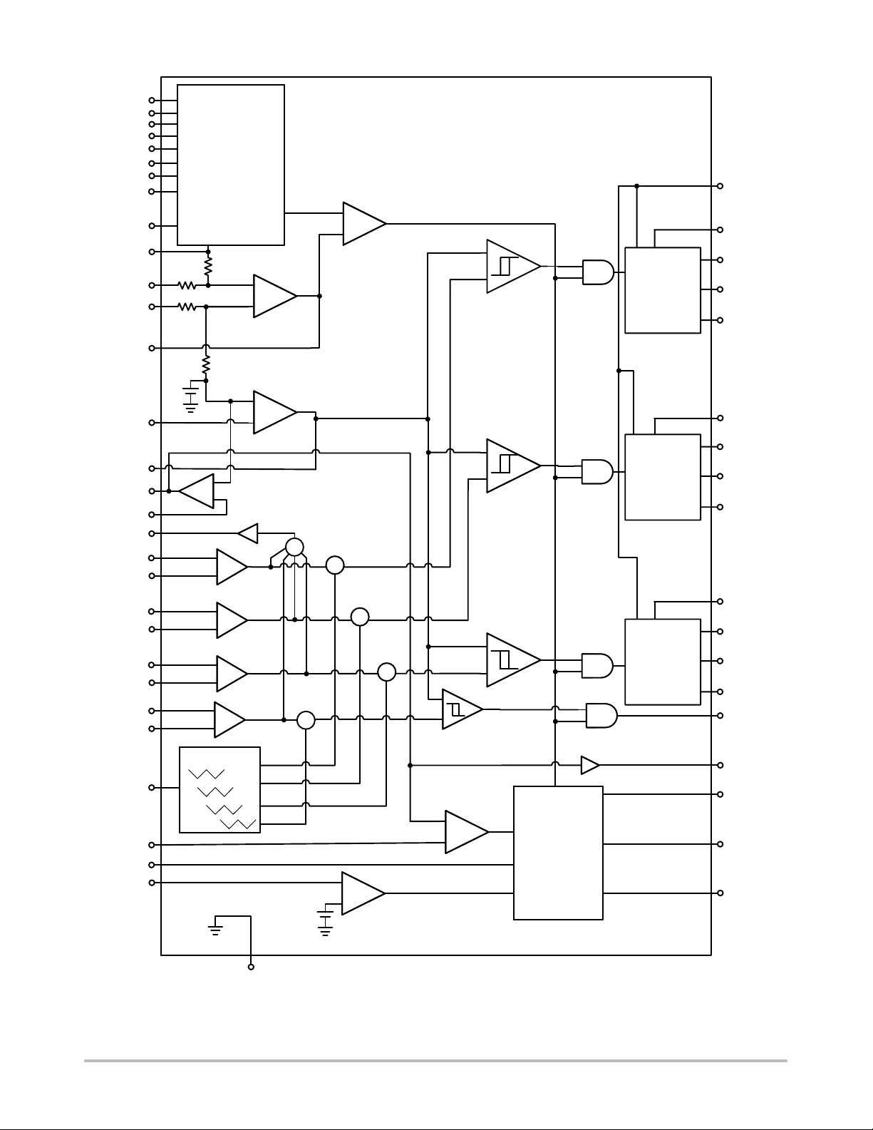
1.3 V
Flexible DAC
Diff Amp
+
-
+
-
Gain = 6
+
-
Gain = 6
+
-
Gain = 6
+
-
Gain = 6
Oscillator
+
Error Amp
+
-
−2/3
NCP5395T
Overvoltage
Protection
+
+
-
+
-
+
+
+
+
+
+
+
-
-
Phase 1
Gate Driver
with
Adaptive
Non−overlap
Phase 2
Gate Driver
with
Adaptive
Non−overlap
Phase 3
Gate Driver
with
Adaptive
Non−overlap
VCCP
BST1
TG1
SWN1
BG1
BST2
TG2
SWN2
BG2
BST3
TG3
SWN3
BG3
G4
IMON
DRVON
ILIM
EN
VCC
GND (FLAG)
+
-
I
Limit
+
4.25 V
-
UVLO
Figure 1. NCP5395T Functional Block Diagram
http://onsemi.com
2
Control,
Fault Logic
and
Monitor
Circuits
12VMON
VR_RDY
VCCP
RFB
RF
CH
CF
CDFB
RDFB
RISO
RT
12V_FILTER
RISO
PSI#_CPU
CFB
RFB
RDRP
R
VID0
VID1
VID2
VID3
VID4
VID5
VID6
VID7
IMON
13
14
15
16
17
18
19
20
21
22
23
24
10
12
11
ILIM
ROSC
IMON
VSP
VSN
DIFFOUT
COMP
VFB
VDRP
VDFB
CSSUM
DAC
12VMON
VCC
8
9
7
6
VID7
VID5
VID6
VID4
NCP5395T
48L 7x7 QFN
FLAG = GND
5
VID2
VID3
3
4
VID1
DRVON
VTT
12V_FILTER
2
1
PSI
BG3
VID0
VBST3
TG3
SWN3
BST2
TG2
SWN2
BG2 41
VCCP
SWN1
TG1
BST1
NCP5395T
48
47
46
45
DRVON
44
43
42
12V_FILTER
40
39
38
37
1
2
21
D
G
S
12V_FILTER
D
G
S
D
G
S
12V_FILTER
D
G
S
PWM3_SENSE_N
PWM3_SENSE_P
+5.0V
VTT
ENABLE
CS4P
25
CS4N
26
CS3P27CS3N
CS2P
28
29
CS2N
30
31
32
33
34
35
G4
36
C17
PWM3_SENSE_P
PWM3_SENSE_N
PWM1_SENSE_P
PWM1_SENSE_N
VR_RDY
BG1
EN
CS1N
CS1P
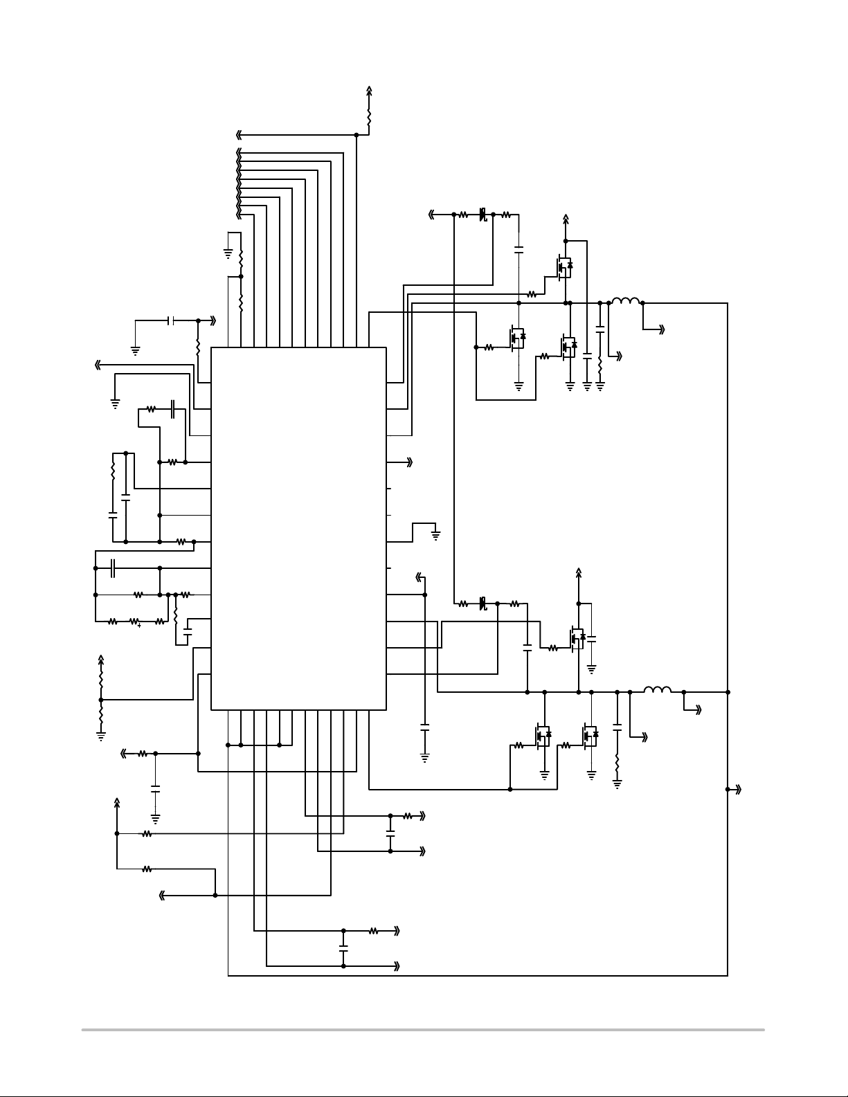
Figure 2. Typical 2 Phase Application
http://onsemi.com
3
D
G
S
D
G
S
PWM1_SENSE_N
PWM1_SENSE_P
VCCP
PSI#_CPU
VID0
VID1
VID2
VID3
VID4
VID5
VID6
VID7
NCP5395T
VTT
R236
12V_FILTER
2 1
12V_FILTER
D
G
S
VCCP
RFB
RF
CH
CF
CDFB
RDFB
RT
RISO
12V_FILTER
+5.0V
VTT
RISO
CFB
RFB
RDRP
R
13
14
15
16
17
18
19
20
21
22
23
24
12
11
10
ILIM
ROSC
IMON
VSP
VSN
DIFFOUT
COMP
VFB
VDRP
VDFB
CSSUM
DAC
12VMON
VCC
CS4N
CS4P
26
25
7
6
8
9
VID7
VID5
VID6
VID4
NCP5395T
48L 7x7 QFN
FLAG = GND
CS2P
CS3P27CS3N
CS2N
29
28
31
30
5
VID2
VID3
CS1N
CS1P
32
4
33
3
VID1
EN
34
1
2
PSI
BG3
VID0
VBST3
TG3
SWN3
DRVON
BST2
TG2
SWN2
BG2
VCCP
SWN1
TG1
BST1
VR_RDY
BG1
G4
36
35
48
47
46
45
DRVON
44
43
42
41
12V_FILTER
40
39
38
37
C37
PWM1_SENSE_P
2
1
21
D
G
S
G
12V_FILTER
D
S
12V_FILTER
D
G
S
D
G
S
D
G
S
G
D
G
S
G
PWM3_SENSE_N
PWM3_SENSE_P
D
PWM2_SENSE_P
S
D
S
PWM2_SENSE_N
VCCP
PWM1_SENSE_N
PWM1_SENSE_P
ENABLE
PWM1_SENSE_N
PWM2_SENSE_P
PWM2_SENSE_N
PWM3_SENSE_P
PWM3_SENSE_N
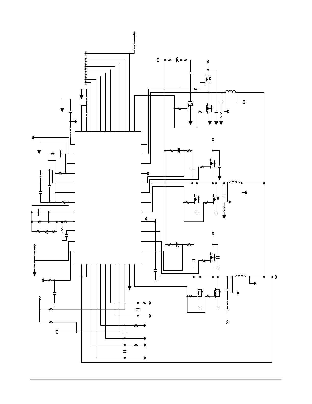
Figure 3. Typical 3 Phase Application
http://onsemi.com
4
12V_FILTER
NCP5395T
VTT
VCCP
RFB
RF
CH
CF
CDFB
RDFB
RT
RISO
12V_FILTER
RISO
PSI#_CPU
IMON
CFB
RFB
RDRP
13
14
16
17
18
19
20
21
22
23
24
15
VID0
VID1
VID2
VID3
VID4
VID5
VID6
VID7
11
12
10
ILIM
ROSC
IMON
VSP
VSN
DIFFOUT
COMP
VFB
VDRP
VDFB
CSSUM
DAC
12VMON
VCC
CS4N
CS4P
26
25
7
8
9
VID7
VID5
VID6
NCP5395T
48L 7x7 QFN
FLAG = GND
CS3P27CS3N
CS2P
28
30
29
6
VID4
VID3
CS1P
CS2N
31
5
VID2
CS1N
32
4
VID1
EN
33
3
34
12V_FILTER
2
1
PSI
BG3
VID0
VBST3
TG3
SWN3
DRVON
BST2
TG2
SWN2
BG2
VCCP
SWN1
TG1
BST1
VR_RDY
BG1
G4
36
35
48
47
46
DRVON
45
44
43
42
41
12V_FILTER
40
39
38
37
1
2
21
21
D
G
S
12V_FILTER
G
G
12V_FILTER
D
G
S
12V_FILTER
D
S
D
PWM3_SENSE_N
S
D
G
S
G
D
G
S
PWM3_SENSE_P
D
PWM2_SENSE_N
PWM2_SENSE_P
S
VCCP
+5.0V
VTT
ENABLE
PWM4_GATE
PWM1_SENSE_P
PWM1_SENSE_N
12V_FILTER
PWM2_SENSE_P
PWM2_SENSE_N
PWM3_SENSE_P
PWM3_SENSE_N
DRVON
PWM4_GATE
PWM4_SENSE_P
PWM4_SENSE_N
2 1
VCC
4
OD
3
IN
2
NCP5359
BST
1
8
7
5
6
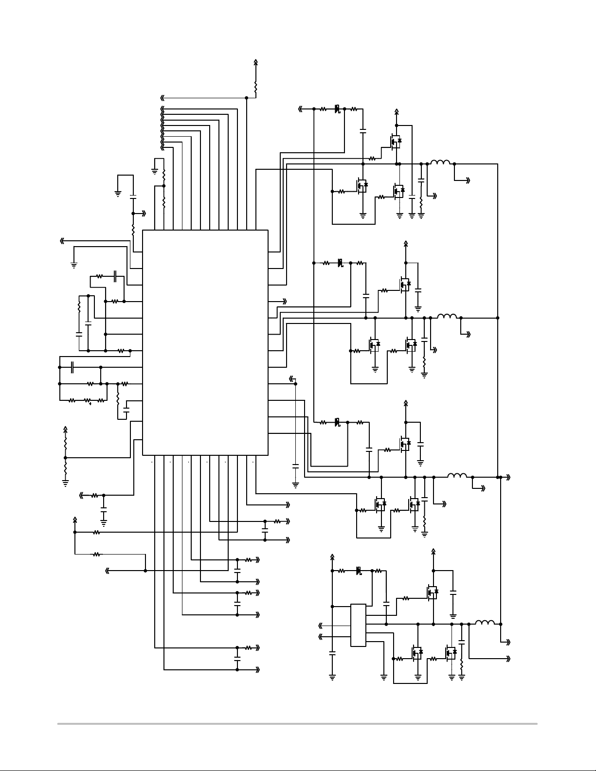
Figure 4. Typical 4 Phase Application
http://onsemi.com
5
D
G
S
DRH
SW
DRL
PGND
D
G
S
12V_FILTER
G
D
G
S
PWM1_SENSE_N
PWM1_SENSE_P
D
S
D
G
PWM4_SENSE_N
PWM4_SENSE_P
S

NCP5395T
Table 1. Pin Descriptions
Pin No. Symbol Description
1 BG3 Low side gate drive #3
2 PSI Power Saving Control. Low = single phase operation; High = normal operation
3 VID0 Voltage ID DAC input
4 VID1 Voltage ID DAC input
5 VID2 Voltage ID DAC input
6 VID3 Voltage ID DAC input
7 VID4 Voltage ID DAC input
8 VID5 Voltage ID DAC input
9 VID6 Voltage ID DAC input
10 VID7/AMD Voltage ID DAC input. Pull to VCC (5 V) to enable AMD 6−bit DAC code.
11 ROSC A resistance from this pin to ground programs the oscillator frequency and provides a 2 V reference
12 ILIM Over current shutdown threshold setting. ILIM = VDRP − 1.3 V. Resistor divide ROSC to set threshold
13 IMON 0 to 1.1 V analog signal proportional to the output load current. VSN referenced Clamped to 1.1 Vmax
14 VSP Non−inverting input to the internal differential remote sense amplifier
15 VSN Inverting input to the internal differential remote sense amplifier
16 DIFFOUT Output of the differential remote sense amplifier
17 COMP Output of the compensation amplifier
18 VFB Compensation amplifier voltage feedback
19 VDRP Voltage output signal proportional to current used for current limit and output voltage droop
20 VDFB Droop Amplifier Voltage Feedback
21 CSSUM Inverted Sum of the Differential Current Sense inputs
22 DAC DAC output used to provide feed forward for dynamic VID
23 12VMON Monitor a 12 V input through a resistor divider
24 VCC Power for the internal control circuits with UVLO monitor
25 CS4P Non−inverting input to current sense amplifier #4
26 CS4N Inverting input to current sense amplifier #4
27 CS3P Non−inverting input to current sense amplifier #3
28 CS3N Inverting input to current sense amplifier #3
29 CS2P Non−inverting input to current sense amplifier #2
30 CS2N Inverting input to current sense amplifier #2
31 CS1P Non−inverting input to current sense amplifier #1
32 CS1N Inverting input to current sense amplifier #1
33 EN Threshold sensitive input. High = startup, Low =shutdown.
34 VR_RDY Open collector output. High indicates that the output is regulating
35 G4 PWM output pulse to gate driver.
36 BG1 Low side gate drive #1
37 BST1 Upper MOSFET floating bootstrap supply for driver#1
38 TG1 High side gate drive #1
39 SWN1 Switch Node #1
40 VCCP Power VCC for gate drivers with UVLO monitor
41 BG2 Low side gate drive #2
42 SWN2 Switch Node #2
43 TG2 High side gate drive #2
44 BST2 Upper MOSFET floating bootstrap supply for driver#2
45 DRVON Bidirectional Gate Drive Enable
46 SWN3 Switch Node #3
47 TG3 High side gate drive #3
48 BST3 Upper MOSFET floating bootstrap supply for driver#3
FLAG GND Power supply return (QFN Flag)
for programming the ILIM voltage.
http://onsemi.com
6

NCP5395T
ABSOLUTE MAXIMUM RATINGS
Rating Symbol Value Unit
ELECTRICAL INFORMATION
BST
V
CCP
− V
SWN
CC
SWN
SWN
Controller Power Supply Voltages to GND
Driver Power Supply Voltages to GND V
High−Side Gate Driver Supplies: BSTx to SWNx V
High−Side FET Gate Driver Voltages: TGx to SWNx VTG − V
Switch Node: SWNx V
Low−Side Gate Drive: BGx VBG − AGND VCC + 0.3 V
Logic Inputs V
GND V
LOGIC
GND
V− GND ±300 mV
Imon Out V
IMON
All Other Pins −0.3, 5.5 V
THERMAL INFORMATION
Thermal Characteristic
R
q
JA
QFN Package (Note 1)
Operating Junction Temperature Range (Note 2) T
Operating Ambient Temperature Range T
Maximum Storage Temperature Range T
Moisture Sensitivity Level
J
AMB
STG
MSL 1
QFN Package
Stresses exceeding Maximum Ratings may damage the device. Maximum Ratings are stress ratings only. Functional operation above the
Recommended Operating Conditions is not implied. Extended exposure to stresses above the Recommended Operating Conditions may affect
device reliability.
*All signals referenced to GND unless noted otherwise.
*The maximum package power dissipation must be observed.
1. JESD 51−5 (1S2P Direct−Attach Method) with 0 LFM
2. Operation at −40°C to 0°C guaranteed by design, not production tested.
−0.3, 7 V
−0.3, 15 V
35 V wrt/GND
40 V ≤ 50 ns wrt/GND
−0.3, 15 wrt/SWN
BOOT + 0.3 V
35 V ≤ 50 ns wrt/GND
−0.3, 15 wrt/SWN
−5 V (200 ns)
35
40 V ≤ 50 ns wrt/GND
−5 VDC
−10 V (200 ns)
−5 V (200 ns)
−0.3, 6 V
0 V
1.1 V
30.5 °C/W
0 to 125 °C
0 to +70 °C
−55 to +150 °C
V
V
V
V
http://onsemi.com
7

NCP5395T
ELECTRICAL CHARACTERISTICS
0°C < TA < 70°C; 0°C < TJ < 125°C; 4.75 < VCC < 5.25 V; All DAC Codes; C
Parameter Test Conditions Min Typ Max Unit
ERROR AMPLIFIER
Open Loop DC Gain
CL = 60 pF to GND,
= 10 kW to GND
R
L
Open Loop Unity Gain Bandwidth CL = 60 pF to GND,
= 10 kW to GND
R
L
Open Loop Phase Margin CL = 60 pF to GND,
= 10 kW to GND
R
L
Slew Rate
DVin = 100 mV, G = −10V/V,
= 1.5 V − 2.5 V,
DV
out
CL = 60 pF to GND,
DC Load = ±125 mA to GND
Maximum Output Voltage 10 mV of Overdrive,
I
SOURCE
= 2.0 mA
Minimum Output Voltage 10 mV of Overdrive,
= 500 mA
I
SINK
Output Source Current 10 mV of Overdrive,
V
= 3.5 V
out
Output Sink Current 10 mV of Overdrive,
V
= 0.1 V
out
DIFFERENTIAL SUMMING AMPLIFIER
V+ Input Pull down Resistance
DRVON = low
DRVON = high
V+ Input Bias Voltage DRVON = low
DRVON = high
Input Voltage Range (Note 3) −0.3 − 3.0 V
−3 dB Bandwidth CL = 80 pF to GND,
= 10 kW to GND
R
L
Closed Loop DC gain VS to Diffout VS+ to VS− = 0.5 V to 1.6 V 0.98 1.0 1.02 V/V
Maximum Output Voltage 10 mV of Overdrive,
I
SOURCE
= 2 mA
Minimum Output Voltage 10 mV of Overdrive,
I
= 1 mA
SINK
Output Source Current 10 mV of Overdrive,
V
= 3 V
out
Output Sink Current 10 mV of Overdrive,
V
= 0.2 V
out
INTERNAL OFFSET VOLTAGE
Offset Voltage to the (+) Pin of the Error Amp & the
VDRP Pin
3. Design guaranteed.
= 0.1 mF unless otherwise noted.
VCC
− 100 − dB
− 18 − MHz
− 70 − °
− 10 −
3.0 − − V
− − 75 mV
1.5 2.0 − mA
0.65 1.0 − mA
−
−
−
0.8
− 15 − MHz
3.0 − − V
− − 0.5 V
1.5 2.0 − mA
1.0 1.5 − mA
−2 0 +2 mV
0.6
6.0
0.05
0.88
−
−
0.1
0.95
V/ms
kW
V
http://onsemi.com
8
 Loading...