

Features of Mobile Subscriber Radio Handset
(LG-ID3100 Type)
1. Wave Type
• G7W
2. Frequency Scope
• Transmit Frequency : 824.820 ~ 848.190MHz
• Receive Frequency : 869.820 ~ 893.190MHz
3. Rated Output Power
• 0.282W(24.5dBm)
4. Output Conversion Method :
5. Voltage and Current Value of Termination Part Amplifier(Catalogue included)
This is possible by correcting the key board channel.
Mode Type Name Voltage Current Power
CDMA SKY77162 3.4V 455mA 0.282W
6. Functions of Major Semi-Conductors
Classification Function
QSC6010 MSM baseband, radioOne RF, and power management.
MCP
(PF38F2040W0YBQ0)
MCP
(PF38F2040W0YBQ0)
7. Frequency Stability
• ±0.5PPM
Z3X-BOX.COM
Flash Memory (64Mbit) ▶ Storing of the mobile station operation
program
PSRAM (32Mbit) ▶ Temporary storing of the data created while
busy
LGE

CDMA MOBILE SUBSCRIBER UNIT
LG-ID3100
SERVICE MANUAL
SINGLE BAND
CDMA MOBILE PHONE
Z3X-BOX.COM

LG-ID3100
Table of Contents
General Introduction
............................................................................................................................................... 2
CHAPTER 1. System Introduction
1. System Introduction ................................................................................................................ 3
2. Features and Advantages of CDMA Mobile Phone .................................................................. 5
3. Structure and Functions of CDMA Mobile Phone ................................................................... 8
4. Specification .............................................................................................................................. 9
5. Installation ............................................................................................................................... 12
CHAPTER 2. Circuit Description
1. RF Transmit/Receive Part ....................................................................................................... 13
2. Digital/Voice Processing Part .................................................................................................. 17
CHAPTER 3. Trouble Shoot
3.1. RX part Trouble .................................................................................................................... 21
3.2. TX part Trouble .................................................................................................................... 24
3.3. Logic part Trouble ................................................................................................................ 28
Appendix
Block Diagram
Circuit Diagram
Component Layout
Total Assy
Z3X-BOX.COM
LGE

LG-ID3100
2/57
LGE Internal Use Only
General Introduction
The LG-ID3100 cellular phone functions as digital cellular phone worked in CDMA (Code Division
Multiple Access) mode.
CDMA mode applies the DSSS (Direct Sequence Spread Spectrum) technique that has been used in
military. This technique enables to share one frequency channel with many users in the same specific
area. As a result, that it increases the capacity 10 times more compared with that in the analog mode
(AMPS) currently used.
Soft/Softer Handoff, Hard Handoff, and Dynamic RF power Control technologies are combined into
this phone to reduce the call being interrupted in a middle of talking over phone.
CDMA digital cellular network consists of MSC (Mobile Switching Office), BSC (Base Station
Controller), BTS (Base station Transmission System), and MS (Mobile Station). Communication
between MS and BTS is designed to meet the specification of TIA/EIA/IS-95-A/B/C (Common Air
Interface). MS meets the specifications of the below :
- TIA/EIA/IS-95-A/B/C (Common Air Interface) : Protocol between MS and BTS
- TIA/EIA/IS-96-B : Speech CODEC
- TIA/EIA/IS-98 : Basic MS functions
- IS-126 : Voice loopback
- TIA/EIA/IS-99 : Short Message Service, Asynchronous Data Service, and G3 Fax Service
LG-ID3100 is composed of a transceiver, a adapter, a Li-Polymer Battery.
Z3X-BOX.COM
LGE

LG-ID3100
3/57
LGE Internal Use Only
CHAPTER 1. System Introduction
1. System Introduction
1.1 CDMA Abstract
The cellular system has a channel hand-off function that is used for collecting the information on the
locations and movements of radio mobile telephones from the cell site by automatically controlling
several cell site through the setup of data transmission routes and thus, enabling one switching
system to carry out the automatic remote adjustment. This is to maintain continuously the call state
through the automatic location confirmation and automatic radio channel conversion when the busy
subscriber moves from the service area of one cell site to that of another by using automatic location
confirmation and automatic radio channel conversion functions. The call state can be maintained
continuously by the information exchange between switching systems when the busy subscriber
moves from one cellular system area to the other cellular system area.
In the cellular system, the cell site is a small-sized low output type and utilizes a frequency allocation
system that considers mutual interference, in an effort to enable the re-use of corresponding
frequency from a cell site separated more than a certain distance. The analog cellular systems are
classified further into an AMPS system, E-AMPS System, NMT system, ETACS system, and JTACS
system depending on technologies used.
Unlike the Time Division Multiple Access (TDMA) or the Frequency Division Multiple Access (FDMA)
used in the band limited environment, the Code Division Multiple Access(CDMA) system which is one
of digital cellular systems is a multi-access technology under the interference limited environment. It
can process more number of subscribers compared to other systems (TDMA system has the
processing capacity three times greater than the existing FDMA system whereas CDMA system,
about 12~15 times of that of the existing system).
CDMA system can be explained as follows: TDMA or SDMA can be used to enable each person to
talk alternately or provide a separate room for each person when two persons desire to talk with each
other at the same time, whereas FDMA can be used to enable one person to talk in soprano, whereas
the other in bass (one of the two talkers can carry out synchronization for hearing in case there is a
bandpass filter function in the area of the hearer).
Another method available is to make two persons to sing in different languages at the same time,
space, and frequency when wishing to let the audience hear the singing without being confused. This
is the characteristics of CDMA.
Z3X-BOX.COM
LGE

LG-ID3100
4/57
LGE Internal Use Only
On the other hand, when employing the CDMA technology, each signal has a different
pseudo-random binary sequence used to spread the spectrum of carrier. A great number of CDMA
signals share the same frequency spectrum. In the perspective of frequency area or time area, several
CDMA signals are overlapped. Among these types of signals, only desired signal energy is selected
and received through the use of pre-determined binary sequence; desired signals can be separated
and then, received with the correlator used for recovering the spectrum into its original state. At this
time, the spectrums of other signals that have different codes are not recovered into its original state
and instead, processed as noise and appears as the self-interference of the system.
LGE
Z3X-BOX.COM

LG-ID3100
5/57
LGE Internal Use Only
2. Features and Advantages of CDMA Mobile Phone
2.1 Various Types of Diversities
When employing the narrow band modulation (30kHz band) that is the same as the analog FM
modulation system used in the existing cellular system, the multi-paths of radio waves create a
serious fading. However, in the CDMA broadband modulation(1.25MHz band), three types of
diversities (time, frequency, and space) are used to reduce serious fading problems generated from
radio channels in order to obtain high-quality calls.
Time diversity can be obtained through the use of code interleaving and error correction code
whereas frequency diversity can be obtained by spreading signal energy to more wider frequency
band. The fading related to normal frequency can affect the normal 200~300kHz among signal bands
and accordingly, serious affect can be avoided. Moreover, space diversity (also called path diversity)
can be realized with the following three types of methods.
First, it can be obtained by the duplication of cell site receive antenna. Second, it can be obtained
through the use of multi-signal processing device that receives a transmit signal having each different
transmission delay time and then, combines them. Third, it can be obtained through the multiple cell
site connection (Soft Handoff) that connects the mobile station and more than two cell sites at the
same time.
2.2 Power Control
The CDMA system utilizes the forward (from a base station to mobile stations) and backward (from
the mobile station to the base station) power control in order to increase the call processing capacity
and obtain high-quality calls. In case the originating signals of mobile stations are received by the cell
site in the minimum call quality level (signal to interference) through the use of transmit power control
on all the mobile stations, the system capacity can be maximized.
If the signal of mobile station is received too strong, the performance of that mobile station is improved.
However, because of this, the interference on other mobile stations using the same channel is
increased and accordingly, the call quality of other subscribers is reduced unless the maximum
accommodation capacity is reduced.
In the CDMA system, forward power control, backward open loop power control, and closed loop
power control methods are used. The forward power control is carried out in the cell site to reduce the
transmit power on mobile stations less affected by the multi-path fading and shadow phenomenon and
the interference of other cell sites when the mobile station is not engaged in the call or is relatively
nearer to the corresponding cell site. This is also used to provide additional power to mobile stations
having high call error rates, located in bad reception areas or far away from the cell site.
The backward open loop power control is carried out in a corresponding mobile station; the mobile
station measures power received from the cell site and then, reversely increases/decreases transmit
power in order to compensate channel changes caused by the forward link path loss and terrain
Z3X-BOX.COM
LGE

LG-ID3100
6/57
LGE Internal Use Only
characteristics in relation to the mobile station in the cell site. By doing so, all the mobile office
transmit signals in the cells are received by the cell site in the same strength.
Moreover, the backward closed loop power control used by the mobile station to control power with
the commands issued out by the cell site. The cell site receives the signal of each corresponding
mobile station and compares this with the pre-set threshold value and then, issues out power
increase/decrease commands to the corresponding mobile station every 1.25 msec (800 times per
second).
By doing so, the gain tolerance and the different radio propagation loss on the forward/backward link
are complemented.
2.3 Voice Encoder and Variable Data Speed
The bi-directional voice service having variable data speed provides voice communication which
employs voice encoder algorithm having power variable data rate between the mobile telephone cell
site and mobile station. On the other hand, the transmit voice encoder performs voice sampling and
then, creates encoded voice packets to be sent out to the receive voice encoder, whereas the receive
voice encoder demodulates the received voice packets into voice samples.
One of the two voice encoders described in the above is selected for use depending on inputted
automatic conditions and message/data; both of them utilize four-stage frames of 9600, 4800, 2400,
and 1200 bits per second. In addition, this type of variable voice encoder utilizes adaptive threshold
values when selecting required data rate. It is adjusted in accordance with the size of background
noise and the data rate is increased to high rate only when the voice of caller is inputted.
Therefore, background noise is suppressed and high-quality voice transmission is possible under the
environment experiencing serious noise. In addition, in case the caller does not talk, data transmission
rate is reduced so that the transmission is carried out in low energy. This will reduce the interference
on other CDMA signals and as a result, improve system performance (capacity, increased by about
two times).
2.4 Protecting Call Confidentiality
CDMA signals have the function of effectively protecting call confidentiality by spreading and
interleaving call information in broad bandwidth. This makes the unauthorized use of crosstalk, search
receiver, and radio very hard substantially. Also included is the encryption function on various
authentication and calls specified in IS-95 for the double protection of call confidentiality.
2.5 Soft Handoff
During the soft hand, the cell site already in the busy state and the cell site to be engaged in the call
later participate in the call conversion. The call conversion is carried out through the original call
LGE
Z3X-BOX.COM

LG-ID3100
7/57
LGE Internal Use Only
connection cell site, both cell sites, and then, new cell site. This method can minimize call
disconnection and prevent the user from detecting the hand-off.
2.6 Frequency Re-Use and Sector Segmentation
Unlike the existing analog cellular system, the CDMA system can reuse the same frequency at the
adjacent cell and accordingly, there is no need to prepare a separate frequency plan. Total
interference generated on mobile station signals received from the cell site is the sum of interference
generated from other mobile stations in the same cell site and interference generated from the mobile
station of adjacent cell site. That is, each mobile station signal generates interference in relation to the
signals of all the other mobile signals.
Total interference from all the adjacent cell sites is the ratio of interference from all the cell sites
versus total interference from other mobile stations in the same cell site (about 65%). In the case of
directional cell site, one cell normally uses a 120°sector antenna in order to divide the sector into
three. In this case, each antenna is used only for 1/3 of mobile stations in the cell site and accordingly,
interference is reduced by 1/3 on the average and the capacity that can be supported by the entire
system is increased by three times.
2.7 Soft Capacity
The subscriber capacity of CDMA system is flexible depending on the relation between the number of
users and service classes. For example, the system operator can increase the number of channels
available for use during the busy hour despite the drop in call quality. This type of function requires
40% of normal call channels in the standby mode during the handoff support, in an effort to avoid call
disconnection resulting from the lack of channels.
In addition, in the CDMA system, services and service charges are classified further into different
classes so that more transmit power can be allocated to high class service users for easier call set-up;
they can also be given higher priority of using hand-off function than the general users.
Z3X-BOX.COM
LGE

LG-ID3100
8/57
LGE Internal Use Only
3. Structure and Functions of CDMA Mobile Phone
The mobile station of CDMA system is made up of a radio frequency part and logic/control (digital)
part. The mobile station antenna is connected with the transmitter/receiver via a SAW duplexer filter
so that it can carry out the transmit/receive function at the same time.
The transmit frequency is the 25MHz band of 824~849MHz, whereas the receive frequency is the
25MHz band of 869~894MHz. The transmit/receive frequency is separated by 45MHz. The RF signal
from the antenna passes the LNA , bandpass SAW filter having the 1.25MHz band and then, is
directly converted into baseband signal by the frequency synthesizer and frequency down converter.
Baseband output signals that have been filtered from spurious signal are converted into digital signals
via an analog-to-digital converters(Rx ADC) and then, sent out respectively to 5 correlators in each
CDMA de-modulator. Of these, one is called a searcher whereas the remaining 4 are called data
receiver(finger). Rx signals include a great number of call signals that have been sent out by the
adjacent cells. These signals are detected with pseudo-noise sequence (PN Sequence). Signal to
interference ratio (C/I) on signals that match the desired PN sequence are increased through this type
of correlation detection process. Then, other signals obtain processing gain by not increasing the ratio.
The carrier wave of pilot channel from the cell site most adjacently located is demodulated in order to
obtain the sequence of encoded data symbols.
During the operation with one cell site, the searcher searches out multi-paths in accordance with
terrain and building reflections. On three data receivers, the most powerful four paths are allocated for
the parallel tracing and receiving. Fading resistance can be improved a great deal by obtaining the
diversity combined output for de-modulation. Moreover, the searcher can be used to determine the
most powerful path from the cell sites even during the soft handoff during the two cell sites. Moreover,
four data receivers are allocated in order to carry out the de-modulation of these paths. Data output
that has been demodulated change the data string in the combined data row as in the case of original
signals(deinterleaving), and then, are de-modulated by the forward error correction decoder which
uses the Viterbi algorithm.
On the other hand, mobile station user information sent out from the mobile station to the cell site pass
through the digital voice encoder via a mike. Then, they are encoded and forward errors are corrected
through the use of convolution encoder. Then, the order of code rows is changed in accordance with a
certain regulation in order to remove any errors in the interleaver. Symbols made through the above
process are spread after being loaded onto PN carrier waves. At this time, PN sequence is selected
by each address designated in each call.
Signals that have been code spread as above are digital modulated (OQPSK) and then, power
controlled at the automatic gain control amplifier (AGC Amp). Then, they are converted into RF band
by the frequency synthesizer synchronizing these signals to proper output frequencies. Transmit
signals obtained pass through the duplexer filter and then, are sent out to the cell site via the antenna.
Z3X-BOX.COM
LGE
LG-ID3100
9/57
LGE Internal Use Only
4. Specification
4.1 General Specification
4.1.1 Transmit/Receive Frequency Interval :
4.1.2 Number of Channels (Channel Bandwidth) :
4.1.3 Operating Voltage :
4.1.4 Battery Power Consumption :
SLEEP IDLE MAX POWER
CDMA
4.1.5 Operating Temperature :
4.1.6 Frequency Stability :
4.1.7 Antenna :
Fixed PIFA Type (Internal), 50
DC 3.2~4.2V
1.2 mA 80 ~ 100 mA 580 mA (25dBm)
-30° ~ +60°
±0.5PPM
DC 3.7V
45MHz
Ω
20CH (BW : 1.23MHz)
4.1.8 Size and Weight
Size : 105.7 x 44 x 16.5mm (L x W x D)
•
Weight : 70g(TBD)
•
4.1.9 Channel Spacing :
4.1.10 Battery Type, Capacity and Orerating Time
Stand-By Time
Talk Time
1.25MHz
Standard (950mAh)
Z3X-BOX.COM
Unit = Hours, Minutes
140 Hrs (SCI=2)
145 Min (Cell power -92dBm)
4.2 Receive Specification
4.2.1 Frequency Range :
869.820 MHz ~ 893.190 MHz
4.2.2 Local Oscillating Frequency Range :
LGE
1738.08MHz ~ 1787.94MHz

LG-ID3100
10/57
LGE Internal Use Only
4.2.3 Intermediate Frequency :
4.2.4 Sensitivity :
4.2.5 Selectivity :
4.2.6 Spurious Wave Suppression :
4.2.7 CDMA Input Signal Range
• Dynamic area of more than -115~ -12.6 dB : 102.4dB at the 1.23MHz band
-104dBm ( C/N 12dB or more)
3dB C/N Degration (With Fch ± 1.25KHz : -30dBm)
QSC60X0 seires (Zero IF)
Maximum of -80dB
4.3 Transmit Specification
4.3.1 Frequency Range :
4.3.2 Intermediate Frequency :
4.3.3 Output Power :
824.820 MHz ~ 848.190 MHz
QSC60X0 seires (Zero IF)
0.282W
4.3.4 Interference Rejection
• Single Tone : -30dBm at 900 kHz
• Two Tone : -43dBm at 900 kHz & 1700kHz
4.3.5 CDMA TX Frequency Deviation :
4.3.6 CDMA TX Conducted Spurious Emissions
• 900kHz : - 42 dBc/30kHz below
• 1.98MHz : - 54 dBc/30kHz below
4.3.7 CDMA Minimum TX Power Control :
Z3X-BOX.COM
±300Hz or less
- 50dBm below
LGE
LG-ID3100
11/57
LGE Internal Use Only
4.4
MS (Mobile Station) Transmitter Frequency
FA NO. CH.NO. CENTER FREQUENCY FA NO. CH.NO. CENTER FREQUENCY
1
2
3
4
5
6
7
8
9
10
1011
29
70
111
152
193
234
275
316
363
824.640 MHz
825.870 MHz
827.100 MHz
828.330 MHz
829.560 MHz
830.790 MHz
832.020 MHz
833.250 MHz
834.480 MHz
835.890 MHz
11
12
13
14
15
16
17
18
19
20
404
445
486
527
568
609
650
697
738
779
837.120 MHz
838.350 MHz
839.580 MHz
840.810 MHz
842.04 MHz
843.270 MHz
844.500 MHz
845.910 MHz
847.140 MHz
848.370 MHz
4.5
MS (Mobile Station) Receiver Frequency
FA NO. CH.NO. CENTER FREQUENCY FA NO. CH.NO. CENTER FREQUENCY
1
1011
869.640 MHz
11
404
882.120 MHz
2
3
4
5
6
7
8
9
10
29
70
111
152
193
234
275
316
363
Z3X-BOX.COM
4.6 Charge time
4.6.1 Standard Battery :
870.870 MHz
872.100 MHz
873.330 MHz
874.560 MHz
875.790 MHz
877.020 MHz
878.250 MHz
879.480 MHz
880.890 MHz
200 Min.
12
13
14
15
16
17
18
19
20
445
486
527
568
609
650
697
738
779
883.350 MHz
884.580 MHz
885.810 MHz
887.04 MHz
888.270 MHz
889.500 MHz
890.910 MHz
892.140 MHz
893.370 MHz
LGE

LG-ID3100
12/57
LGE Internal Use Only
5. Installation
5.1 Installing a Battery Pack (Soft Pack type)
1) The soft battery pack is keyed so it can only fit one way. Align the groove in the battery pack with
the rail on the back of the phone until the battery pack rests flush with the back of the phone.
2) Insert the bottom of battery into the openning on the back of the phone. Then, push the battery
cover up until the latch clicks.
5.2 For Adapter Use
1) Plug the adapter into a wall outlet. The adapter can be operated from either a 110V or a 220V
source.
2) Insert the adapter jack into the phone with the installed battery pack.
Red light indicates battery is being charged. Green light indicates battry is fully charged
5.3 For Mobile Mount
5.3.1 Installation Position
In order to reduce echo sound when using the Hands-Free Kit, make sure that the speaker and
microphone are not facing each other and keep microphone a generous distance from the speaker.
5.3.2 Cable Connections
5.3.2.1 Power and Ignition Cables
Connect the red wire to the car battery positive terminal and the black wire to the car ground. Connect
the green wire to the car ignition sensor terminal. ( In order to operate HFK please make sure to
connect green wire to ignition sensor terminal.) Connect the kit’s power cable connector to the
interface box power receptacle.
5.3.2.2 Antenna Cable Connection
Connect the antenna coupler cable connector from the cradle to the external antenna connector. ( Antenna is not
included.)
Z3X-BOX.COM
LGE

LG-ID3100
13/57
LGE Internal Use Only
CHAPTER 2. Circuit Description
1. RF Transmit/Receive Part
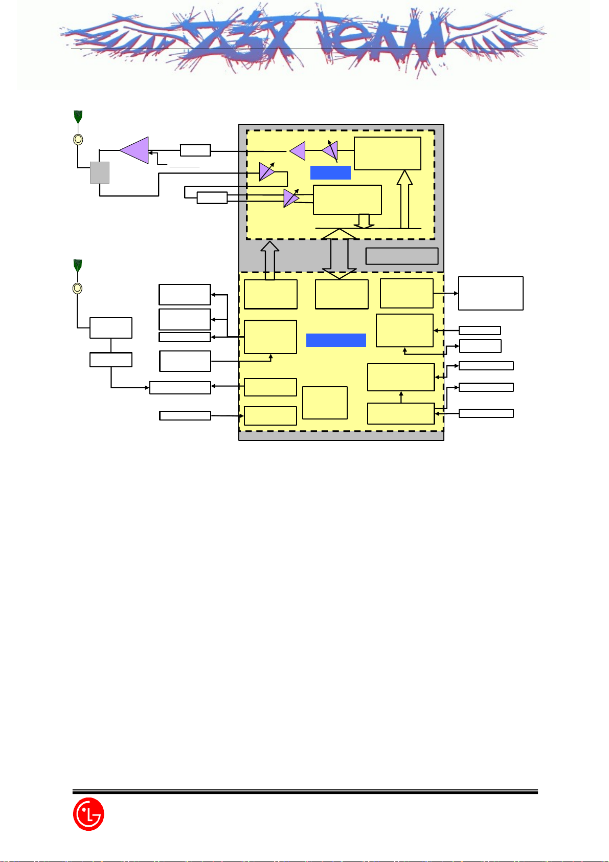
1.1 Overview
The RF transmit/receive part employs the direct conversion architecture (ZIF, Zero Intermediate
Frequency). The transmit/receive frequency is respectively 824.04~848.97MHz and 869.04~893.97
MHz. The block diagram is shown in [Figure 3-1].
RF signals received through the antenna are fed QSC6010 through the duplexer. And then, they pass
the low noise amplifier (LNA), combined with the signals of local oscillator (VCO) at the frequency
mixer in order to create baseband signal directly.
Baseband signals created are changed into digital signals by the analog / digital converter (ADC, A/D
Converter) and then, auto gain controlled and, are demodulated by the modulator / demodulator.
In the case of transmission, QSC6010 modulates, interpolates, and converts the digital signal into an
analog baseband before upconverts the Tx analog baseband into RF.
The baseband quadrature signals are upconverted to the Cellular Tx frequency bands and amplified to
provide signal drive capability to the power amp.
After that, the RF signal is amplified by the Power Amp in order to have enough power for radiation.
Finally, the RF signal is sent out to the cell site via the antenna after going through the duplexer
Z3X-BOX.COM
LGE
LG-ID3100
14/57
LGE Internal Use Only
RF500(U101)
Mobile S/W
IL : 0.4~0.5dB
ANT
TX
DUP
SKY77162(U102)
PA
B9426(F110)
IL=1.5~2.3 dB
BPF
V ref=2.85V
[Figure 2-1] Block Diagram Of ID3100
Quadrature
LNA
RF Block
Upconverter
RX
EFSD836MF1S2(DP101)
TX IL 1.5 ~ 2.3 dB
RX IL 2.3 ~ 3.5 dB
ANT(Headset)
FM
Receiver
AMP
Keypad
Backlight
Backlight
Viblator
Keypad
SPK/Earpiece
BPF
EFCH881MTCA7(F103)
IL = 1.5~2.0 dB
LCD
MIC
Output
Voltage
Reguration
User
Interface
SPK AMP
I/F
(MIC/EAR)
1.2 Description of Receive Part Circuit
Quadrature
Downconverter
RF
Interface
BB & PM Block
Codec
QSC6010
Memory
Interface
Input Power
Management
Connectivity
General
Housekeeping
MCP
64Mb X 32Mb
DC 5V
Battery
UIM
UART
19.2M OSC
1.2.1 Duplexer (DP101)
The duplexer consists of the receive part bandpass filter (BPF) and the transmit part bandpass filter
(BPF) which have the function of separating transmit/receive signals in the full duplex system using
the transmit/receive common antenna. The transmit part BPF is used to suppress noises and spurious
waves entering the receive band among transmit signals in order to prevent the drop in receive
sensitivity characteristics. The receive part BPF blocks the signals sent out from entering the receive
end in order to improve sensitivity characteristics.
Insertion loss (IL) in the transmit band is 2.8dB (Max), whereas IL in the receive band is 3.5dB (Max).
The receive band attenuation amount of transmit filter is 45dB (Min) and the transmit band attenuation
amount of receive filter is 57dB or more (Min).
LGE
Z3X-BOX.COM

LG-ID3100
15/57
LGE Internal Use Only
1.2.2 Rx RF SAW FILTER (F101)
The main function of Rx RF SAW filter is to attenuate mobile phone spurious frequency, attenuate
noise amplified by the LNA and suppress second harmonic originating in the LNA.
1.2.3 Down-Converter Mixers (U201)
The QSC6010 device performs signal direct-down-conversion for Cellular applications. It contains all
the circuitry (with the exception of external filters) needed to support conversion of received RF
signals to baseband signals. The LO Buffer Amplifier buffers the RF VCO to the RF Transmit
Upconverter. QSC6010 offers the most advanced and integrated CDMA Rx solution designed to meet
cascaded Noise Figure (NF) and Third-order Intercept Point (IIP3) requirements of IS-98C and
J-STD-018 specifications for Sensitivity, Two-Tone Intermodulation, and Single-tone Desense.
Operation modes and band selection are specially controlled from the Mobile Station Modem QSC6010.
1.3 Description of Transmit Part Circuit
1.3.1 Description on the Internal Circuit of QSC6010(U201)
For the transmit data path(Tx), the QSC6010 modulates, interpolates, and converts the digital signal
into an analog baseband, and upconverts the Tx analog baseband into RF. The QSC6010
communicates with the external RF and analog baseband to control signal gain in the RF Rx and Tx
signal paths, educe base band offset errors, and tune the system frequency reference.
The QSC6010 baseband-to-RF Transmit Processor performs all Tx signal-processing functions
required between digital baseband and the Power Amplifier Module (PAM). The baseband quadrature
signals are upconverted to the Cellular frequency bands and amplified to provide signal drive
capability to the PAM. The QSC6010 includes an mixer for up-converting analog baseband to RF, a
programmable PLL for generating Tx and Rx LO frequency, cellular driver amplifier and Tx power
control. As added benefit, the single sideband upconversion eliminates the need for a band-pass filter
normally required between the upconverter and driver amplifier.
Z3X-BOX.COM
I, I/, Q and Q/ signals are modulated by Offset Quadrature Phase Shift King (OQPSK). I and Q are 90
deg. out of phase, and I and I/ are 180 deg. The mixer in QSC6010 converts baseband signals into
RF signals. After passing through the upconverters, RF signal is inputted into the Power Amplifier
Module.
The QSC6010 Cellular CDMA RF specifications are described below:
LGE

LG-ID3100
16/57
LGE Internal Use Only
Condition Min. Typ. Max. Unit
Maximum Output Power
Noise power
ACPR
1.3.2 Power Amplifier (U102)
The power amplifier that can be used in the CDMA mode has linear amplification capability.
For higher efficiency, it is made up of one module (Monolithic Microwave Integrated Circuit) for which
RF input terminal and internal interface circuit are integrated onto one IC after going through the GaAs
HBT (heterojunction bipolar transistor) process.
The module of power amplifier is made up of an output end interface circuit including this module.
The maximum power that can be inputted through the input terminal is 8dBm and conversion gain is
about 28.5dB. RF transmit signals that have been amplified through the power amplifier are sent to
the duplexer.
869-894 MHz, all power
±885kHz, < 2:1 VSWR
±1.98MHz, < 2:1 VSWR
28 dBm
-135.0 dBm/Hz
levels
-44
-57
dBc
dBc
1.4 Description of Frequency Synthesizer Circuit
1.4.1 Crystal Oscillator (X202)
Crystal Unit generates the refrence frequency of 19.2MHz. Tolerance at 25°C is ±12x10-6
Max.Tolerance over the tmperature range is ±12x10-6 Max. at -30 to 85°C
Z3X-BOX.COM
LGE

LG-ID3100
17/57
LGE Internal Use Only
2. Digital/Voice Processing Part
2.1 Overview
The digital/voice processing part processes the user's commands and processes all the digital and
voice signal processing in order to operate in the phone. The digital/voice processing part is made up
of a keypad/LCD, receptacle part, voice processing part, mobile station modem part, memory part,
and power supply part.
2.2 Configuration
2.2.1 Keypad/LCD and Receptacle Part
This is used to transmit keypad signals to QSC6010. It is made up of a keypad backlight part that
illuminates the keypad, LCD part that displays the operation status on to the screen, and a receptacle
that receives and sends out voice and data with external sources.
2.2.2 Voice Processing Part
The voice processing part is made up of an audio codec in QSC6010 used to convert MIC signals into
digital voice signals and other external MIDI Synthesizer used to convert digital voice signals into
analog voice signals, amplifying parts for amplifying the voice signals and MIC signals are on external
MIDI Synthesizer and Codec in QSC6010.
2.2.3 QSC6010 (Mobile Station Modem) Part
QSC6010 is the core elements of a CDMA mobile station and carries out the functions of CPU,
encoder, interleaver, deinterleaver, Viterbi decoder, Mod/Demod, codec, and vocoder.with RF, and PA
module
2.2.4 Memory Part
Z3X-BOX.COM
The memory part is made up of a flash memory, SRAM for storing data.
LGE

LG-ID3100
18/57
LGE Internal Use Only
2.3 Circuit Description
2.3.1 Keypad/LCD and Receptacle Part
Once the keypad is pressed, the key signals are sent out to QSC6010 for processing. In addition,
when the key is pressed, the keypad lights up through the use of 8 LEDs and LCD backlights up. The
status and operation of a mobile station are displayed on the screen for the user with the characters
and icons on the LCD.
Receptacle(CON404) exchanges audio signals and data with external sources and external power.
Battery Connector receives power from the battery.
2.3.2 QSC Part
The baseband circuits and system software incorporate a low-power, high-performance
RISC microprocessor core featuring the ARM926EJ-S™ CPU and Jazelle™ accelerator
circuit from ARM® Limited. There are two low-power, high-performance QDSP4000™
digital signal processor (DSP) cores, one for the modem and one for applications. Camera
functions are supported by the QSC6030 device only, and MIDI and MP3 functions are
supported by the various QSC tiers as indicated in Table 1-2.
The baseband function reduces part costs by using two external bus interfaces to support
next-generation memory architectures such as NAND FLASH, SRAM and pseudo SRAM
(PSRAM), page and burst mode NOR or MLC NOR FLASH. The EBI2 also serves as an
enhanced LCD interface.
A variety of connectivity options are supported: the keypad interface and USB, UART, and
RUIM ports are available.
A camera interface is provided; this feature is available in the QSC6030 device only (not
the QSC6020 or QSC6010 devices).
Audio support supplements the analog/RF function’s CODEC, including up to
32- polyphonic MIDI in the QSC6010 device, MP3, AAC and AAC+ decoding support in
the QSC6020 and QSC6030 devices and additionally a Compact Media Extension
(CMX™)/MIDI synthesizer, and QCELP®.
Z3X-BOX.COM
The CDMA air interfaces mentioned earlier are implemented on the baseband CDMA
processor. All necessary interfaces to the RF functions are provided, some using a portion
of the 57 GPIOs. Many of the AMSS-configurable GPIOs are available for alternate uses
as desired by the wireless product designers.
Support circuitry and baseband internal functions include security, clock generation and
distribution, JTAG/ETM test interfaces, mode and reset controls, and the Q-fuse.
LGE

LG-ID3100
19/57
LGE Internal Use Only
2.3.2.1 Audio Processing Part
MIC signals are inputted into the audio codec, and amplified with programmable gain, and converted
into digital signals(PCM). Then, they are inputted into QSC6010.
In addition, digital audio signals(PCM) outputted from QSC6010 are converted into analog signals
after going through the audio codec. These signals are amplified with programmable gain on codec’s
internal AMP and external MIDI Synthesizer, transferred to the ear-piece.
2.3.3 Memory Part
The memory part consists of a 64Mbits Flash Memory and a 32Mbits SRAM. On the Flash Memory,
there are programs used for the operation of a mobile station and the non-volatile data of the mobile
station such as a ESN(Electronic Serial Number) are stored. The programs can be changed through
down loading after the assembling of mobile stations. On the SRAM, data generated during the
operation of a mobile station are stored temporarily.
2.3.4 Power Supply Part
When the battery voltage (+4.2V) is fed and the PWR key of keypad is pressed, the power-up circuitry
in QSC6010(U201) is activated by the PWR_ON_SW/ signal, and then the LDO regulators embedded
in QSC6010 are operated and +2.80V_MSMC, +2.85V_MSMP and +2.6V_MSMA are generated.
Z3X-BOX.COM
LGE

LG-ID3100
20/57
LGE Internal Use Only
2.3.5 Logic Part
The Logic part consists of internal CPU of QSC6010, MCP (SRAM+FLASH ROOM).
The QSC6010 receives X-tal(19.20MHz) clock signals, and then controls the phone during the CDMA
mode. The major components are as follows:
CPU : ARM926EJ-S microprocessor core
MEMORY :
FLASH ROM : 64Mbits (U301, PF38F2040W0YBQ0)
•
STATIC RAM : 32Mbits (U301, PF38F2040W0YBQ0)
•
CPU
The ARM7TDMI 32-bit microprocessor is used and CPU controls all the circuitry. Some of the
features of the ARM microprocessor include a 3 stage pipelined RISC architecture, both 32-bit ARM
and 16-bit THUMB instruction sets, a 32-bit address bus, and a 32-bit internal data bus. It has a high
performance and low power consumption.
FLASH ROM and SRAM
Flash Memory is used to store the program of the mobile station. Using the down-loading program,
the program can be changed even after the mobile station is fully assembled.
SRAM is used to store the internal flag information, call processing data, and timer data.
KEYPAD
For key recognition, key matrix is setup using KEY_SENSE[0]-[4] signals and GPIO of output ports
of QSC6010. 8 LEDs and backlight circuitry are included in the keypad for easy operation in the
dark.
LCD MODULE
LCD module contains a controller which will display the information onto the LCD by 16-bit data
from the QSC6010. It is also supplied stable 1.8V_MSM_E1 by inner regulator in U201 for fine view
angle and and LCD reflects to improve the display efficiency.
Z3X-BOX.COM
LGE

LG-ID3100
21/57
LGE Internal Use Only
CHAPTER 3. Trouble Shooting
CHAPTER 3. Trouble Shooting
3.1 Rx Part Trouble
When Rx Sensitivity isn’t good enough
Test Point
TP1
TP2
TP3
Z3X-BOX.COM
LGE

LG-ID3100
22/57
LGE Internal Use Only
Circuit Diagram
TP1
TP2
LGE
Z3X-BOX.COM
TP3

LG-ID3100
23/57
LGE Internal Use Only
Checking Flow
Rx TEST SETUP(HHP)
- Test Channel : 610
E5515C Setup
START
- CH : 610
1. Check
RF cable & Loss
2. Check RF path
Circuit connection
3. Check
TP1(U101), TP2(DP101),
TP3(F101)
Z3X-BOX.COM
NG
Change RF cable or re-set loss
NG
Re-work or replace them
NG
Replace them
Replace QSC6010 or main board
Download S/W &
LGE
Calibrate
NG

LG-ID3100
24/57
LGE Internal Use Only
3.2 Tx part Trouble
Test Point
QSC6010
TX
filter
Duplexer
PAM
Mobile
S/W
Checking Flow
START
√ Connect the phone to UART connector
√ Press H/W or F7, then click ‘offline-d’
-Click ‘Band select‘ to cdma & Tx on &Power Amp
On
-Set channel to 610 & AGC :400
√ Spectrum analyzer setting
√ Oscilloscope setting
1. Check
PAM Circuit
Z3X-BOX.COM
2. Check
Duplexer & Mobile SW
Circuit
LGE
3. Check
QSC6010 circuit
√ Redownload SW, CAL

LG-ID3100
25/57
LGE Internal Use Only
3.2.1 Check PAM Circuit
Test Point
TP3, TP4
(Vcc1,2)
TP5
(RF_OUT)
TP2
(Vref +2.85V)
Circuit Diagram
TP1
(RF_IN)
TP3
TP4
TP5
Z3X-BOX.COM
TP1
TP2
LGE

LG-ID3100
26/57
LGE Internal Use Only
Circuit Flow
Check U102 TP1(Pin2)
Check U102 TP3, TP4(Pin1,8)
Waveform
RF_IN
Check U102 TP2(Pin4)
V_ref
VCC1,2
Check U102 TP5(Pin7)
RF_OUT
Input Level is Appear?
YES
Is Vref 2.85V ?
YES
Level is
3.2V~4.2V OK?
YES
Output Level
is Appear?
YES
PAM Circuit is OK
See next page to check
Duplexer & Mobile SW
Or Replace QSC6010
NO
NO
NO
NO
Check F110 circuit
Check Q101 circuit
Check C203, U201
Replace U102
SPECTRUM ANALYZER CONDITION
-RBW : 1MHz,VBW: 1KHz
-Span : 60MHz
-Frequency : DCN( 836.52MHz)
Z3X-BOX.COM
U102 Pin2 DCN PAM_IN U102 Pin7 DCN PAM_OUT
LGE

LG-ID3100
27/57
LGE Internal Use Only
3.2.2 Check Duplexer & Mobile SW
TEST POINT
DP101
Mobile S/W
U101 TP2(PIN1)
Mobile S/W in
DP101 TP1(PIN6)
DP_out
Circuit Diagram
Circuit Flow
Check DP101 Pin6
DUP_OUT
Check U101 Pin1
TP2(PIN1)
TP1(PIN6)
Z3X-BOX.COM
Level is Appear?
YES
Level is Appear?
NO
NO
Replace DP101
Replace U101
LGE
YES
Replace QSC6010
LG-ID3100
28/57
LGE Internal Use Only
3.3 Logic Part Trouble
3.3.1 Power On Trouble
Circuit Diagram
TP2
TP6
TP7
TP1
Test Points
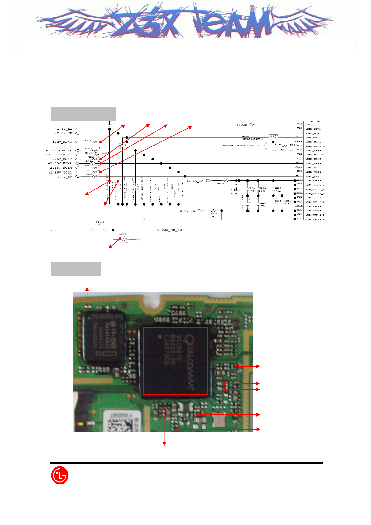
TP1(R404) : PWR_ON_SW
TP3
Figure 3.3.1 QSC6010 circuit diagram
TP5TP4
LGE
Z3X-BOX.COM
TP4(R244) : +2.65V_MSMA
U201
QSC6010
TP3(R217) : +2.6V_MSMP
TP7(C225) : +2.6V_TX
TP6(C255) : +2.6V_RX
TP2(R224) : +1.2V_MSMC
TP5(R236) : +2.85V_TCXO

LG-ID3100
29/57
LGE Internal Use Only
Checking Flow
START
YES
Check Battery Voltage
> 3.2V ?
YES
Push power-on key and check
the level change of
TP1(R404)
YES
Check the voltage of
the following port at U201
TP2(+1.2V_MSMC)
TP3(+2.6V_MSMP)
TP4(+2.65V_MSMA)
TP6(+2.85V_TCXO)
TP6(+2.6V_RX)
TP7(+2.6V_TX)
NO
NO
Charge of Change Battery and try again
Check the contact of power-key
or dome switch
Replace U201
NO
YES
Z3X-BOX.COM
Re-download Software
LGE

LG-ID3100
30/57
LGE Internal Use Only
3.3.2 Charging Trouble
Test Points
TP2(U201)
: QSC6010
TP1(CON404)
Circuit Diagram
Figure 3.3.2 Charging PART
TP1(CON404)
TP3
TP2(U201)
Z3X-BOX.COM
LGE

LG-ID3100
31/57
LGE Internal Use Only
Checking Flow
SETTING : Connect the battery and the charging adaptor (TA) to the phone
START
YES
Charging Connector
TP1(CON404)
Well-soldered?
YES
Voltage at
TP3(Pin25(V_CHAR))
of TP1(CON404)
=5V ?
YES
Check TP2(U201) circuit
YES
Is the battery
charged
NG
NO
NO
NO
Re-solder or replace
TP1(CON404)
The charging adaptor (TA) is out of order.
Change the charging adaptor.
Replace TP2(U201) or
mainboard
The battery may have the problem
Change the battery and try again.
YES
Charging will operate properly
LGE
Z3X-BOX.COM

LG-ID3100
32/57
LGE Internal Use Only
3.3.3 Audio AMP Trouble
Test Points
TP1
QSC_AMP_OUT-
TP2
QSC_AMP_OUT+
Circuit Diagram
U309
TP3
COM_SPK-
U308
TP4
COM_SPK+
Figure 3.3.3 RECEIVER PART
TP2
LGE
TP1
TP4
Z3X-BOX.COM
TP3

LG-ID3100
33/57
LGE Internal Use Only
Checking Flow
SETTING : “Ringers” at Sounds menu
START
Does Speaker work Properly?
Yes
NO
Check the contact of speaker or
Replace the speaker
Check the signal
TP1, TP2 of U308,
U309
Yes
Check the signal
level at TP3, TP4
of U308, U309
Yes
Z3X-BOX.COM
NO
NO
Replace U201(QSC6010) or board
Re-soldering or
Replace the U308, U309
Speaker will work properly
LGE

LG-ID3100
34/57
LGE Internal Use Only
3.3.6 MIC Trouble
Test points
TP1
R326
TP2(MIC +)
Circuit Diagram
U302(MIC)
TP1
TP3
(C321)
U201
(QSC6010)
TP3
Z3X-BOX.COM
LGE
TP2(MIC +)

LG-ID3100
35/57
LGE Internal Use Only
Checking Flow
SETTING : After initialize 5515C, Test US Cellular
START
Voltage at TP1 = 1.2V?
(MIC BIAS Voltage Check)
Yes
Check the signal level
at TP2 of U302(MIC)
Is It a few tens mV(AC)?
Yes
Check the soldering of
TP3(C321)
Yes
Does MIC work Properly? Replace U201(QSC6010)
Yes
MIC will work properly
No
No
No
Check the soldering
Of R326
Yes
Replace U201(QSC6010)
Replace the U302(MIC)
Re-solder TP3(C321)
No
No
Re-solder R326
LGE
Z3X-BOX.COM

LG-ID3100
36/57
LGE Internal Use Only
3.3.7 Vibrator Trouble
Test points
TP1(D301)
TP2(C324)
Figure 3.3.7 Vibrator PART
Checking Flow
Circuit Diagram
TP2
Figure 3.3.7 VIBRATION CONTROL BLOCK
SETTING : “Vibrator on” at Sounds of test menu
START
TP1
Check the state of
Contact of Vibrator
Yes
Does Vibrator work Properly?
No
No
Re-contact vibrator
Replace Vibrator
Z3X-BOX.COM
Yes
Check the solder of
TP1,TP2
OK
Replace U201(QSC6010)
LGE
or board
NG
Re-solder or replace them

LG-ID3100
37/57
LGE Internal Use Only
3.3.8 Key Backlight LED Trouble
Test Points
TP1
TP9
Figure 3.3.8 KEYPAD BACK LIGHT PART
Circuit Diagram
TP5
TP6
TP2
TP7
TP3
TP4
TP8
TP1
TP2TP3TP4TP5 TP6TP7 TP8
TP9
LGE
Z3X-BOX.COM
Figure 3.3.8 KEYPAD Back Light Circuit

LG-ID3100
38/57
LGE Internal Use Only
Checking Flow
START
Turn on the phone
OK
NG
Charge or Change Battery and try again
NG
No
No
Check the soldering of each Resister or
Replace them.
Re-solder or replace LEDs
Replace U201(QSC6010)
Is the voltage level of
(TP1~TP8)
3.2-4.2V?
Yes
Check LEDs’ directions
OK
Check the signal level at
TP9(KYPD_EN)=high?
Yes
BACKLIGHT WILL
WORK PROPERLY
Z3X-BOX.COM
LGE

LG-ID3100
39/57
LGE Internal Use Only
3.3.9 Earphone Trouble
Test Points
TP8
(R392)
TP4
TP12TP13
TP7
TP3
Circuit Diagram
TP6
TP7
TP4
TP1
CON301
TP2
TP3
TP10
TP11
TP11
TP5
U311
TP6
TP10
TP9
(R393)
TP12
TP9
TP13
Z3X-BOX.COM
TP1
TP2
TP8
LGE

LG-ID3100
40/57
LGE Internal Use Only
Checking Flow
SETTING : After initialize 5515C, Test US Cellular
START
Insert the earphone to the handset.
Yes
Earphone detect problem
Does the audio
Profile of the phone change to
the earphone mode?
Yes
Set the audio part of the test
equipment to echo mode
Yes
Can you hear your voice
from the earphone?
Yes
4
Z3X-BOX.COM
Audio path problem
No
Change the earphone and
Can you hear your voice
from the earphone?
Change Earphone.
try again.
Yes
Yes
No
No
1
Set the audio part of the
test equipment to
continuous wave mode
Yes
Can you hear the sound
from the earphone?
Yes
3
Earphone sending
Earphone receiving
Path problem
No
2
path problem
Earphone will
work properly
LGE

LG-ID3100
41/57
LGE Internal Use Only
Earphone detect problem
1
Change the earphone and then
insert to the handset
Level of TP1 of CON301
is less than 1.4V?
No
Check soldering
the CON301
Yes
Change the main board
or QSC6010
Yes
No
Does the audio
Profile of the phone change to
the earphone mode?
Re-download software
Yes
4
Does it work well?
Re-solder or replace CON301
No
No
Yes
4
Replace QSC6010
LGE
Z3X-BOX.COM

LG-ID3100
42/57
LGE Internal Use Only
Earphone sending path problem
3
Level of TP2 at CON301
is more than 2.0V
Yes
Level of TP5(C279) is
About a few tens
or hundreds mVAC?
Yes
No
No
Re-solder
TP3, TP4
Re-solder
TP5(C279)
Earphone receiving path problem
2
Signwave appear
at TP6 and TP7 of U311
No
Change main board
Does it work well?
Yes
Yes
4
No
Re-download
Does it work well?
Replace QSC
software
No
Signwave appear
at TP8 and TP9?
Yes
Signwave appear at
TP12 and 13 of CON301?
Yes
4
LGE
Yes
No
Z3X-BOX.COM
No
Level of TP10 and 11
of U311 is Low?
(High: FM Mode)
No
Re-download S/W
Check the receiving path from U311 to CON301
Yes
Check the condition of U311
If problem, replace the U311

LG-ID3100
43/57
LGE Internal Use Only
3.3.10 LCD Trouble
Test Points
Pin2
CON406
Pin1
Circuit Diagram
Pin35
TP1
TP3
U303
TP2
Pin1
TP2
Z3X-BOX.COM
LGE
TP3
TP1

LG-ID3100
44/57
LGE Internal Use Only
Checking Flow : LCD
START
Check the LCD FPCB connection
OK
NG
Re-connect LCD FPCB
Check the TP1 of CON406
(MSMP)= 2.6V ?
Yes
Check the
CON406 Soldering
Yes
Check the
Control signal
D[0:15], LCD_RESET/,
LCD_ID, LCD_CS/
,LCD_LIGHT
Z3X-BOX.COM
OK
No
No
Check & replace QSC6010 circuit
Re-Soldering CON406
NG
Does R405~R476
(LCD connection)
Work Properly?
Yes
No
Re-soldering or Replace
R405~R476
Change the LCD Module
LGE
Change the Main Board

LG-ID3100
45/57
LGE Internal Use Only
Checking Flow : Back Light
START
Check the TP2 of U303,
+VPWR
Yes
Does U303 work Properly?
Yes
Check the signal level at
TP3(LCD_BACK_EN)=high?
Yes
LCD backlight will
work properly
No
No
No
Check & replace QSC
Re-Soldering or
Replace U303
Replace QSC
LGE
Z3X-BOX.COM

LG-ID3100
46/57
LGE Internal Use Only
3.3.11 UIM Trouble
Test Points
TP1(CON302)
TP2
U201
(QSC6010)
TP4
Circuit Diagram
TP2
Z3X-BOX.COM
TP3
TP5
TP3
TP4
TP1
TP5
LGE

LG-ID3100
47/57
LGE Internal Use Only
Checking Flow
TP1
TP2, TP3, TP4, TP5
Z3X-BOX.COM
TP1
LGE

LG-ID3100
48/57
LGE Internal Use Only
3.3.12 FM Radio Trouble
Test Points
Pin1
TP1
Circuit Diagram
X101
Q102
TP2
TP3
(R139)
TP4
U104
TP4
(R138)
TP6
TP5
TP6
TP2
Frequency Generator Circuit FM Receiver Circuit FM AMP Circuit
LGE
Z3X-BOX.COM
TP1
TP3
TP5

LG-ID3100
49/57
LGE Internal Use Only
Checking Flow
SETTING : Attach the headset and “Listen to Radio” at Radio menu
Start
Check the Freq. at
TP1 of Q102
Freq.= 32.768kHz?
(Shown Graph 1)
Yes
Audio signal
appear at
TP3,TP4?
Yes
Audio signal
appear at TP5
and TP6 of
U104?
Yes
No
No
No
X101 is working?
Check the TP2 of
X101.
Freq.= 32.768kHz?
Yes
Check the condition of Q102
and external component.
Check the FM Receiver circuit,
input voltage, soldering.
If problem, replace the defected
component.
Check the FM AMP circuit.
If problem, replace the defected
component.
No
Replace X101
Refer to Earphone Trouble part.
LGE
Z3X-BOX.COM
Graph 1. FM Radio Clock

ID3100 Block Diagram
50/57
LGE Internal Use Only
RF500(U101)
Mobile S/W
IL : 0.4~0.5dB
ANT
TX
DUP
SKY77162(U102)
PA
B9426(F110)
IL=1.5~2.3 dB
BPF
V ref=2.85V
Quadrature
Upconverter
LNA
RF Block
RX
EFSD836MF1S2(DP101)
TX IL 1.5 ~ 2.3 dB
RX IL 2.3 ~ 3.5 dB
ANT(Headset)
FM
Receiver
AMP
EFCH881MTCA7(F103)
IL = 1.5~2.0 dB
Keypad
Backlight
LCD
Backlight
Viblator
Keypad
SPK/Earpiece
BPF
Quadrature
Downconverter
QSC6010
Output
Voltage
Reguration
User
Interface
BB & PM Block
RF
Interface
Z3X-BOX.COM
SPK AMP
Memory
Interface
Input Power
Management
Connectivity
64Mb X 32Mb
DC 5V
Battery
MCP
UIM
UART
MIC
I/F
(MIC/EAR)
Codec
General
Housekeeping
19.2M OSC

Doc. Name Doc. Number SHEET :
ID3100 1/4
TX Line : 824Mhz ~849Mhz
RX Line : 869Mhz ~ 894Mhz
FM Radio
51/57
LGE Internal Use Only
LG-RD3000/RD3100 MAIN
DRAW :
DATE
CHKD
APRD
REF
MAN
ISSUE :
CONTENT :
R115, R108 :DEL
C104,C106 :DEL
ANT Change
L108: DNI-> 10n
L105: DNI-> 15n
C115: 0R -> 3.9p
FM external AMP
C127/C128 ->180p
R140/R141 ->68k
REV1.0
FM ANT Change
C159 100p->8.2nH
ANT Change
L108: 10nH->12nH
C115: 3.9p->8.2p
L105: 15n ->DNI
OR DEL
R155
REV1.1
ANT_MATHING
<ANT>
ANT101
ANT-RD2330
C115
9p
RF500
U101
+
1
2
-
L108
12n
L105
DNI
1005
IN(ANT)
OUT(DUP)
Q101
+VPWR
C101
C121
1608
10u-10V
2.2u
SYF-1A106MZF-RP
DP101
34
EFSD836MF1S2
C126
100p
L106
10n
3
TX
GND1
GND2
GND3
6
ANT
GND4
GND5
GND6
RX
1
33p
C113
C102
DNI
1005
U102
L103
3.3n
C109
DNI
C118
2p
1005
2
4
5
7
8
9
SKY77162
G_DUMMY
1
VCC1
2
RF_IN
3
VCONT
4
VREF
9
C110
100p
L104
6.8n
L107
DNI
1005
8
VCC2
7
RF_OUT
6
GND2
5
GND1
L111
8.2n
KRX102U
4
3
1
2
5
C116 100p
R105
DNI
1005
C124
10n
R128
DNI
1005
PA_R0
C120
1n
LNA_IN
<RF Tx PATH>
+2.85V_TCXO
PA_ON
R104
18
L101
330
C103
10p
L113
2
5
G1
G2
IN
4
OUT
1
IN
3
B9426
R106
330
F110
1.8p
L115
1.8p
C119
10p
CELL_OUTP
CELL_OUTM
<RF Rx PATH>
+2.6V_RX
C107
C156
12n
1
0.1u
L117
4.7n
F101
EFCH881MTCA7
IN
G1
L112
100n
C108
100p
R103
1k
C117
100p
C155
DNI
1005
3
OUT
4
OUT/
G2
2
5
L116
2.2n
C111
6p
L114
22n
C123
6p
LNA_OUT
MIX_INM
L110
82n
L109
L102
2.2n
82n
MIX_INP
1 OF 4
T.H.KIM
2007.04.10
H.T.KIM
C115: 8.2p -> 9p
REV1.2_Change
TX_SAW FILTER
RD3000_FM_RADIO _ DEL
C158
4
22p
X101
SSP-T7-F(12.5PF_+/-20PPM)
2
1
C157
22p
<FM RECEIVER>
R133
30
U103
SI4702-B16
C159
1
FM_ANT
8.2n
Z3X-BOX.COM
FM_RESET/
R131
10M
1608
Q102
TC7SZU04AFE
1
2
3
1.2k
R129
R130
1.2k
5
VCC
NC
A
4
Y
GND
R132
300k
+3.0V_FM
NC1
2
FMIP
3
RFGND
4
GND1
5
RST
R154
10k
20
6
NC2
SEN
19
SCLK7SDIO8RCLK
16
VA
11
GPIO317GPIO218GPIO1
VD
12
GND2
13
ROUT
14
LOUT
15
GND3
VIO
G_SLUG
9
21
10
10k
10k
R137
R136
R135
R134
FM_GPIO2
+3.0V_FM
C160
100n
C166
C167
47n
R138
47n
R139
20k
20k
FM_AMP_EN
C161
100n
+3.0V_FM
+3.0V_FM
FM_I2C_SDA
30
FM_I2C_SCL
30
C127
120p
R140
100k
LM4809LDX-NOPB
1
5
3
4
9
C128
120p
R141
100k
U104
VIN1
VIN2
GND
SHUTDOWN
GND_SLUG
BYPASS
VOUT1
VOUT2
8
6
7
VDD
2
C162
470n
+3.0V_FM
C163
2.2u
1608
FM_AFR
FM_AFL
C103,C119:10p
L113,L115:1.8p
Rev.12
LGE Proprietary LG<41>-A-2011.0
Duplication of this document and the use or communication of the contents thereof are forbidden without express authority. Offenders are punishable and liable to the payment of damages. All rights are reserved in the event of the grant of a patent or the registration of a utility model.
LGE

Doc.Name
ID3100 2/4
Power Line
Audio Line
MIC Line
52/57
LGE Internal Use Only
TX_CP
C213
C246
8.2n
C260
220p
+/-1%
R209
15k
19.2 M Crystal Change
X202
NX3225SA(EXS00A-CS00179)
4
C204
DNI
1005
1
V_CHAR
+2.6V_RX
+2.6V_TX
+1.2V_MSMC
+1.8V_MSM_E1
+2.9V_MSM_E2
+2.6V_MSMP
+2.65V_MSMA
+2.85V_RUIM
+2.85V_TCXO
+3.0V_FM
TYPE Range
Buck / 300mA ON / 1.3V 0.75 ~ 3.05V - Core
MSMP / 300mA ON / 2.6V 1.5 ~ 3.05V - PAD FOR I/O
MSMA / 150mA ON / 2.6V 1.5 ~ 3.05V - Analog
MSME1 / 150mA ON / 1.8V 0.75 ~ 3.05V - EBI1 Circuits
MSME2 / 150mA ON / 2.9V 0.75 ~ 3.05V - EBI2 Circuits
RFRX / 150mA OFF/ 2.6V 1.5 ~ 3.05V - RF RX
RFTX / 150mA OFF/ 2.6V 1.5 ~ 3.05V - RF TX
RUIM / 150mA OFF/ 2.85V 1.5 ~ 3.05V - RUIM
(1.8V & 3.0V Support)
TCXO / 50mA ON / 2.85V 1.5 ~ 3.05V - XO
USB / 50mA OFF/3.3V 3.0V ~ 6.1V - USB Circuit--
<PCB REVISION>
+2.6V_RX
PCB REVISON ADC
Revison R265 R266 ADC_Volt
C 100K 5.6K 0.15V
D 100K 12K 0.30V
E 100K 20K 0.45V
F 100K 27K 0.60V
1.0 100K 36K 0.75V
1.1 100K 47K 0.90V
1.2 100K 56K 1.05V
1.3 100K 75K 1.20V
1.4 100K 100K 1.40V
LGE Proprietary
+VPWR
R235
10k
R224
R207
R268
R217
R244
R212
R236
R269 0
Condition
R265
100k
C216
1u
1608
Q201
2SB1424
3
E
1
B
C
2
R227
0.1
+/-1%
2012R
C203
DNI
2012
C285
10u-10V
0
0
C280
DNI
1005
0
0
0
0
1608
2.2u-6.3V
1608
2.2u-6.3V
C255
C225
C281
33n
R266
56k
3.3n
C239
47n
R234
12k
+/-1%
3
C241
DNI
1005
2
PWR_ON_SW/
JTAG_PSHOLD
+VPWR
1n
4.7u 2012
1608
1608
1608
2.2u-6.3V
2.2u-6.3V
C217
C202 DNI
C240
C248
PCB_REV
Duplication of this document and the use or communication of the contents thereof are forbidden without express authority. Offenders are punishable and liable to the payment of damages.
All rights are reserved in the event of the grant of a patent or the registration of a utility model.
1608
2.2u-6.3V
2.2u-6.3V
C214
C269
+1.8V_MSM_E1
+2.9V_MSM_E2
+2.6V_MSMP
+2.65V_MSMA
LG-RD3000/RD3100 MAIN
RX_CP
PA_ON
PA_R0
CELL_OUTM
CELL_OUTP
TX_CP
+2.85V_TCXO
TP206
150mA ->
225 ~500mA ->
0.1u
C201
C233
0.1u
0.1u
C209
C207
0.1u
0.1u
C218
C245
0.1u
C229
0.1u
C232
0.1u
+VPWR
L202
MIP2520D4R7M
Current is not used ->
+2.6V_RX
R271
0
2.2u-6.3V
R228 0
C264
100p
C266
2.2u-6.3V
1608
1608
C221
R218
0
L201
22n
L203
C263
22n
100p
DNI
R270
C228
1608
100p
C222
C278
C206
0.1u
0.1u
0.1u
C251
0.1u
C253
C261
0.1u
0.1u
C230
C252
C256
C227
0.1u
0.1u
0.1u
0.1u
1u
1u
1608
C284
C250
+2.6V_TX
+1.2V_MSMC
+/-1%
11.8k
R215
LNA_IN
LNA_OUT
MIX_INM
MIX_INP
RX_CP
+/-1%
R240
5.76k
TEMP_ADC
BATT_ADC
PCB_REV
KYPD_EN/
VIB_EN/
1n
C236
4.7u
1608
C234
C257
DNI
2
1
R245
1005
C237
C271
100p
100p
C210
C267
C223
0.1u
0.1u
100p
2.2u-6.3V
C249
C277
C244
C235
0.1u
0.1u
0.1u
C275
0.1u
C272
C238
C224
0.1u
0.1u
0.1u
< JTAG POINT >
CON201
JTAG_STANDARD_10PIN
Doc.Number SHEET OF
DRAW
TP203
D[11]
D[15]
D[14]
D[13]
D[12]
A[1]
A[2]
F4
EBI_D_15H4EBI_D_14H5EBI_D_13H7EBI_D_12J4EBI_D_11H2EBI_D_10
FAILED_TB/GPIO(34)
GND_A_AN1
M7
A13
1005
R210
DNI
+2.6V_MSMP
D[10]
GND_A_AN2
GND_A_AN3
GND_A_AN4
GND_A_AN5
GND_A_AN6
A14
D11
D14
E11
E16
<TP ARRAY>
D[2]
D[5]
D[4]
D[6]
D[8]
D[9]
D[3]
D[7]
J5
EBI_D_9H1EBI_D_8J7EBI_D_7K4EBI_D_6K2EBI_D_5J8EBI_D_4K5EBI_D_3K7EBI_D_2K8EBI_D_1L4EBI_D_0
QSC6010
GND_A_AN7
GND_A_AN8
GND_A_AN9
GND_A_GR1
GND_A_GR2
GND_A_RF1_1
GND_A_RF1_2
H13
H14
H15
G15
L15
K18
K19
L16
U202
UART-TP
1
GND
2
UART-RXD
3
UART-TXD
4
V_CHAR
5
ON_SW
6
VBATT
7
USB-POWER
8
USB-RXD
9
USB-TXD
10
CHAR_MON
11
KEY_LED_EN
12
NC1
A[7]
A[5]
A[6]
A[3]
A[4]
A[8]
A[9]
A[10]
A[11]
A[21]
A[22]
A[20]
H11
G10
H10
EBI_A_24
EBI_A_23E8EBI_A_22D9EBI_A_21
Y1
PA_ON
AA3
PA_R0
L22
CELL_OUTM
M22
CELL_OUTP
J22
TX_CP
K16
RBIAS_TX
A18
LNA_IN
B21
LNA_OUT
D22
MIX_INM
E22
MIX_INP
G22
RX_CP
B20
RBIAS_LNA
R13
TRK_LO_ADJ
T15
XO_TUNE
R14
TCXO_OUT
AB19
XTAL_19M_IN
AB20
XTAL_19M_OUT
W22
XTAL_32K_IN
Y22
XTAL_32K_OUT
B12
HKAIN0
D12
HKAIN1
R21
MPP1
R22
MPP2
M15
CBL_PWR_N
N16
KPD_PWR_N
R15
PS_HOLD
P15
KPD_DRV_N
P16
VIB_DRV_N
R16
LCD_DRV_N
N15
VDD_IN1
P18
VDD_IN2
T19
VDD_IN3
U19
VDD_IN4
V14
VDD_IN5
W14
VDD_IN6
W21
VDD_IN7
AA18
VDD_IN8
AB14
VDD_IN_CORE
W15
VCOIN
1005
V15
VCHG
W16
CHG_CNT_N
AA15
ISNS_P
AA16
ISNS_M
W17
BAT_FET_N
V16
VBAT
T21
VREG_RFRX
T22
VREG_RFTX
AA14
VSW_MSMC
AB15
VREG_MSMC
DNI
W13
VREG_MSMC_S
V21
VREG_MSME1
V22
VREG_MSME2
P19
VREG_MSMP
AB12
VREG_MSMA
AA13
VREG_RUM
N11
VREG_TXCO
AB18
VREG_USB
A20
VDD_RFRX1
C21
VDD_RFRX2_1
D21
VDD_RFRX2_2
E21
VDD_RFRX2_3
F22
VDD_RFRX3_1
G21
VDD_RFRX3_2
H18
VDD_RFRX4
H22
VDD_RFTX1_1
J21
VDD_RFTX1_2
K21
VDD_RFTX1_3
K22
VDD_RFTX2
N22
VDD_RFTX3
N19
VDD_RFTX5
N21
VDD_RFTX4_1
P21
VDD_RFTX4_2
P22
VDD_RFTX4_3
B5
VDD_CORE1
B11
VDD_CORE2
J2
VDD_CORE3
T12
VDD_CORE4
U2
VDD_CORE5
AA6
VDD_CORE6
AA8
VDD_CORE7
B4
VDD_P1_1
B7
VDD_P1_2
B9
VDD_P1_3
G2
VDD_P2_1
L2
VDD_P2_2
B10
VDD_P3_1
P2
VDD_P3_2
V2
VDD_P3_3
V13
VDD_P3_4
EBI_A_20A8EBI_A_19E9EBI_A_18B8EBI_A_17G9EBI_A_16E4EBI_A_15D4EBI_A_14D5EBI_A_13E5EBI_A_12F5EBI_A_11D6EBI_A_10
VDD_P3_5
VDD_P3_6
VDD_A_AN1
VDD_A_AN2
VDD_A_AN3
VDD_A_AN4
AA5
B13
E12
E13
E15
G13
AA10
C212
470p
R225
47k
VDD_A_AN5
A[12]
A[17]
A[14]
A[15]
A[13]
A[16]
A[18]
A[19]
G7
EBI_A_9D7EBI_A_8H8EBI_A_7B6EBI_A_6E6EBI_A_5A6EBI_A_4G8EBI_A_3D8EBI_A_2H9EBI_A_1E7EBI_A_0
Z3X-BOX.COM
VDD_A_AN6
VDD_B_AN1
VDD_B_AN2V9TRST_N
TCK
TMS
TDI
TDOW9RTCK
PON_RESET_N
RESIN_N
RESOUT_N
RSRVD
WDOG_EN
MODE_1
MODE_0
G14
H12
L10
T10
AB9
T11
R10
EBI_MODEP5TRUSTED_BOOT/GPIO(16)
T14
T13
AA9
W10
V11
W11
V10
W12
10k
R230
1005
R246 DNI
RESIN/
TDO
TMS
TDI
1
TDI
2
TMS
3
4
TDO
5
TRST_N
6
R255
TCK
10
7
+2.6V_MSMP
8
RESIN/
9
JTAG_PSHOLD
10
RTCK
TRST_N
TCK
+2.6V_MSMP
RTCK
D[0]
D[1]
L7
EBI_RESOUT_N
U201
GND_A_RF1_3
GND_A_RF1_4
GND_A_RF1_5
L18
L19
N2
G4
EBI_WE_NG5EBI_OE_NF2EBI_LB_NE1EBI_UB_N
GPIO(15)/EBI_MEM_CLK
GND_A_RF1_6
GND_A_RF1_7
GND_A_RF1_8
L21
M16
M18
M19
GND_A_RF1_9
GND_A_RF1_10
M21
V_CHAR
UB/
D1
A10
EBI_CS6_N
GPIO(22)/EBI_CS7_N
GND_A_RF2_1
GND_A_RF2_2
GND_A_RF2_3
G18
G19
H19
MSM_DP_RXD
MSM_DP_TXD
PWR_ON_SW/
+VPWR
TP31_PU
C1
D10
GPIO(26)/EBI_CS5_N
GND_A_RF2_4
H21
RAM_CS6/
EBI_RESOUT/
LB/
WE/
OE/
M8
M2
EBI_CS4_N
EBI_CS2_N
GPIO(31)/EBI_CS3_N
GND_A_RF2_5
GND_A_RF2_6
GND_A_RF3_1
J18
J19
F18
ROM_CS0/
LCD_FLM
N1
M1
B3
EBI_CS0_NF1EBI_BSY_N
EBI_WAIT_N
GPIO(25)/EBI_CS1_N
GND_A_RF3_2
GND_A_RF3_3
GND_A_RF4_1
F19
F21
D17
D18
LCD_CS/
A3
L1
L8
A1
NC1A2NC2B1NC3
LCD_ENL5LCD_RS
LCD_CS_N
EBI_ADV_N
GND_A_RF4_2
GND_A_RF4_3
GND_A_RF4_4
GND_A_RF4_5
GND_A_RF4_6
GND_B_AN1
GND_B_AN2
D19
E17
E18
E19
G12
K11
<Battery Level>
+VPWR
AA1
AB1
NC4
NC5
GND_B_AN3A5GND_B_CORE1
K12
R239
470k
AB2
NC6
GND_B_CORE2
J1
A11
AA22
AB21
NC7
NC8
GND_B_CORE3
GND_B_CORE4U1GND_B_CORE5
R12
AB22
A22
B22
NC9
NC10
GND_B_CORE6
GND_B_CORE7A4GND_B_DIG1A7GND_B_DIG2A9GND_B_DIG3
AB6
AB8
R241
470k
C22
A19
A21
B18
B19
K13
L13
M13
N10
N12
E10
DNC4
DNC5
DNC6
DNC7
UART2_TX_D/UIM_DATA/GPIO(11)
UART2_RFR_N/UIM_CLK/GPIO(10)
UART2_CTS_N/UIM_RESET/GPIO(9)
BACKLIGHT_EN/GP_PDM_0/GPIO(8)
GND_B_DIG7P1GND_B_DIG8
GND_B_DIG9V1GND_B_DIG10
M10
R11
G11
DNC8
DNC9
DNC10
DNC11
UART1_RFR_N/GPIO(56)
UART1_CTS_N/GPIO(55)
CAM_DATA_7/GPIO(53)
CAM_DATA_6/GPIO(52)
CAM_DATA_5/GPIO(51)
CAM_DATA_4/GPIO(50)
CAM_DATA_3/GPIO(49)
CAM_DATA_2/GPIO(48)
CAM_DATA_1/GPIO(47)
CAM_DATA_0/GPIO(46)
CAM_PCLK/GPIO(42)
CAM_HSYNC/GPIO(43)
CAM_VSYNC/GPIO(44)
CAM_FLASH/GPIO(33)
GP_MN/GPIO(30)
RINGER/GPIO(29)
GP_PDM_2/GPIO(21)
UART2_RX_D/GPIO(20)
I2C_SCL/GPIO(19)
I2C_SDA/GPIO(18)
HEADSET_DET_N/GPIO(7)
PCM_CLK/SDAC_CLK/GPIO(6)
PCM_DOUT/SDAC_DOUT/GPIO(5)
PCM_DIN/SDAC_MCLK/GPIO(4)
PCM_SYNC/SDAC_L_R/GPIO(3)
KYPD_17/GPIO(1)
KYPD_15/GPIO(2)
KYPD_13/MSM_DP_DTR/GPIO(36)
KYPD_11/GPIO(0)
KYPD_9/GP_PDM_1/GPIO(12)
KEYSENSE_4N/GPIO(38)
KEYSENSE_3N/GPIO(39)
KEYSENSE_2N/GPIO(40)
KEYSENSE_1N/GPIO(41)
KEYSENSE_0N/GPIO(37)
KYPD_MEMO/GPIO(17)
GND_B_DIG11
GND_B_DIG12
GND_B_SR1
GND_B_SR2
GND_B_SR3
AB5
G16
H16
J15
AB10
GND_P_SPKR1
GND_P_SPKR2
GND_P_DRVR1
GND_P_DRVR2
GND_B_SR4
J16
GPIO(54)
GPIO(45)
GPIO(35)
GPIO(32)
GPIO(28)
GPIO(27)
GPIO(23)
GPIO(24)
GPIO(14)
GPIO(13)
UART1_RX_D
UART1_TX_D
USB_VBUS
MIC_BIAS
SPKR_IN_P
SPKR_IN_M
SPKR_OUT_P
SPKR_OUT_M
REF_ISET
GND_P_RF1
GND_P_RF2
GND_MSMC
GND_P_GEN1
GND_P_GEN2
GND_P_GEN3
GND_TCXO
GND_B_SR9
GND_B_SR8
GND_B_SR7
GND_B_SR6
GND_B_SR5
K15
HPH_OUT
REF_BYP
REF_GND
M4
N8
U4
Y2
V5
V7
U5
W4
W8
W5
V6
W6
V8
W7
T7
W2
AB3
AB11
V4
N5
B2
C2
D2
M5
N4
P8
P7
T2
E2
R1
AA11
AA12
V12
N7
R2
T1
T8
R9
AB7
AA4
AB4
W18
USB_ID
AB16
USB_DP
AB17
USB_DM
AA17
AA7
T9
AA2
R7
P4
T4
R4
T5
R5
W1
R8
D15
MIC1N
D16
MIC1P
B16
MIC2N
B17
MIC2P
A17
D13
A15
EAR1OP
A16
EAR1ON
B14
AUXOP
B15
AUXON
U21
U22
V19
W19
E14
CCOMP
AA21
AA20
AA19
V18
Y21
T18
R19
U18
N18
AB13
V17
T16
R18
N13
M12
M11
L12
L11
SIGN107237501
C205
82n
C279
C247 82n
C258
C254
C208 0.1u
C242
R216
C276
FM_AMP_EN
FM_RESET/
LT_DETECT/
EARSPK/FM_EARMOD
RCV/SPK_MODE
FM_GPIO2
HFSO/
TP207
BATT_DET/
DC_PWR_SEN/
TP28
LCD_RESET/
EARPHONE_KEY
F_WP/
FM_I2C_SCL
FM_I2C_SDA
LCD_ID
UIM_DATA
UIM_CLK
UIM_RESET/
LCD_BACK_EN
EAR_SENSE/
AUX_PCM_CLK
AUX_PCM_DOUT
AUX_PCM_DIN/
AUX_PCM_SYNC
MSM_DP_RXD
MSM_DP_TXD
KYPD[17]
KYPD[15]
KYPD[13]
KYPD[11]
KYPD[9]
KEY_SENSE[4]
KEY_SENSE[3]
KEY_SENSE[2]
KEY_SENSE[1]
KEY_SENSE[0]
MIC+
82n
0.1u
0.1u
100p
C268
220n
22
R233
R256
0.1u
5.6k
R257
5.6k
+/-1%
121k
EAR_MIC
MIC_BIAS
EAR_SPK
EAR10P
EAR10N
C219
FM_AFR
0.1u
C220
0.1u
QSC_AMP_OUT+
QSC_AMP_OUT-
4.7
4.7
R267
R243
0.1u
C265
0.1u
C282
NC11
NC12
DNC1
DNC2
DNC3
GND_B_DIG4G1GND_B_DIG5K1GND_B_DIG6
A12
<TEMP. CHECK>
R223
80.6k
BATT_ADC
C259
68n
+2.85V_TCXO
+/-1%
R226
R214
470k
+/-1%
1608
1
2
NCP18WM154J03RB
TEMP_ADC
C226
68n
DATE
CHKD
APRD
REF
MAN
ISSUE
CONTENT
R222 :DEL
+VPWR C285 DNI inserted
REV1.0
OR DEL
R248,R250,R238,R211,R242
2 4
T.H.KIM
2007.04.10
H.T.KIM
Rev.12
LGE
LG<41>-A-2011.0

+2.9V_MSM_E2
53/57
LGE Internal Use Only
Doc. Name Doc. Number SHEET :
<MEMORY>
DNI
1005
C356
R395 0
R330
DNI
C337
100p
1608
C306
100n
C310
2.2u-6.3V
A[1]
A[2]
A[3]
A[4]
A[5]
A[6]
A[7]
A[8]
A[9]
A[10]
A[11]
A[12]
A[13]
A[14]
A[15] D[14]
A[16]
A[17]
A[18]
A[19]
A[20]
TP305
A[21]
TP301
OE/
ROM_CS0/
DNI
1005
R306
A2
G1
A0
DU5A1DU6
F1
A1
E1
A2
D1
A3
B1
A4
C1
A5
F2
A6
E2
A7
F6
A8
D7
A9
E7
A10
B8
A11
C8
A12
D8
A13
F7
A14
E8
A15
F8
A16
D2
A17
B2
A18
B3
A19
E6
A20
B7
A21
C7
A22
C3
A23
D3
A24
E3
A25
J2
F1_OE3
K1
F1_CE#
H8
F2_OE#
G8
F2_CE#
K3
F3_CE#
DU1M1DU2M2VSS1B4VSS2C4VSS3L1VSS4L2VSS5L5VSS6L6VSS7L7VSS8L8DU3M7DU4
<MOTOR>
+VPWR
CON303
1
LA4-436BK
2
1
C324
10n
D301
C346
KDS160E
DNI
C345
33p
+2-
1005
VIB_EN/
LG-RD3000/RD3100 MAIN
J8
K6
K4
A8
DQ0
VCCQ1L3VCCQ2K7VCCQ3
PF38F2040W0YBQ0
F1_VCC1B5F1_VCC2L4F2_VCC1B6F2_VCC2
U301
DU7A7DU8
P_VCCK5S_VCC
M8
+VPWR
LCD_BACK_EN
F_WP#
F_RST#
F_WE#
F_VPP
R_WE#
R_UB#
R_LB#
R_OE#
S_CS1#
S_CS2
P_MODE
P1_CS#
P2_CS#
DQ1
DQ2
DQ3
DQ4
DQ5
DQ6
DQ7
DQ8
DQ9
DQ10
DQ11
DQ12
DQ13
DQ14
DQ15
CLK
ADV#
WAIT
+1.8V_MSM_E1
1608
C342
R304
C340
2.2u-6.3V
R303
DNI
1005
R397
R312
TP_D0
D[0]
D[1]
D[2]
D[3]
D[4]
D[5]
D[6]
D[7]
D[8]
D[9]
D[10]
D[11]
D[12]
D[13]
D[15]
F_WP/
UB/
LB/
OE/
DNI
10n
RAM_CS6/
100p
WE/A[22]
R311
DNI
1005
TP_WE/
TP302
TP303
C341
100n
H2
H3
G3
H4
J5
G5
J6
H7
G2
J3
G4
J4
H5
G6
H6
J7
C6
E5
E4
F4
F5
D4
G7
D5
F3
C2
H1
J1
C5
R302
4.7k
K8
D6
K2
DNI
1005
<LCD Back Light>
U303
AAT3157ITP-T1
10
1608
1u
C302
C311
1k
C1+
9
C1-
5
VIN
4
GND
11
EN/SET
12
NC
1608
C305
1u
< AUDIO PART >
QSC_AMP_OUT+
EAR10P
QSC_AMP_OUT-
EAR10N
EBI_RESOUT/
Power Line
Audio Line
MIC Line
C303
7
C2+
6
C2-
8
VOUT
1
D1
2
D2
3
D3
1u
1608
1608
+VPWR
C301
U308
NLAS4157DFT2G
1
B1
2
GND
R364
3
B0
12
C338
1n
R365
C339
1n
U309
NLAS4157DFT2G
1
B1
2
GND
3
B0
12
+VPWR
EAR_SPK
FM_AFR
FM_AFL
0.1u
6
S
5
VCC
4
A
6
S
VCC
A
R310
5
100n
4
C3441u
1608
RCV/SPK_MODE
R309
100n
COM_SPK+
COM_SPK-
R390 DNI 1005
R333
DNI
1005
U311
NLAS5223BMNR2G
1
VCC
5
NC1
7
NC2
2
NO1
10
NO2
COM_SPK+
DNI
1005
C315
COM_SPK-
C334
33p
C335
33p
3
COM1
9
COM2
4
IN1
8
IN2
6
GND
HP_R
HP_L
EARSPK/FM_EARMOD
ID3100 3/4
U306
EMS1810TPB1P
1
+
2
-
DRAW :
DATE
CHKD
APRD
REF
MAN
ISSUE :
CONTENT :
Rev.10
HP_R R390 INSERT
Value Change
留
EAR_POP UP Noise
R392,R393 0R->75R
Rev.1.1
C311: 10k -> 1k
Rev.1.2
R397_DNI INSERT
TP_POINT_INSERT
R395 o ohm INSERT
C356 DNI INSERT
<EAR MIC JACK>
R392
R393
75
KRA304E
R339
1.2k
75
22u-6.3V
TCSCS0J226KAAR
U305
R352
C329
10n
TCSCS0J226KAAR
C322
E
B
C
4.7k
L307
C343
BLM15HD182SN1
22u-6.3V
1
L305
CIM05J601NC
100k
R396
100k
C314
R398
C307
10n
RD3000 EARPHONE
L308
2
BLM15HD182SN1
1
CIM05J601NC
FM_ANT
6.8n
L304
270n
1608
L306
2
2
3
6
5
4
1
KJA-PH-0-0147
C308
ICVL0518100Y500FR
CON301
HP_R : C343, L307, R398 : DEL
L305, L306, L308 -> 1005 0R
R341
10u-6.3V
TCSCS0J106MPAR
HP_R
HP_L
EAR_SENSE/
EAR_MIC
1k
C327
+2.65V_MSMA
+2.65V_MSMA
LCD_LIGHT
LED1
LED2
1u
C304
EARPHONE_KEY
3 OF 4
T.H.KIM
2007.04.10
H.T.KIM
Rev.12
L304, -> 1608 0R
R326
2.2k
<MIC>
R379
ICVL0505101V150FR
C317
4.7n
<Around QSC>
C321
82n
MIC+
DNI
1005
R319
R301
10
1
1
+
+
2
-
2
LED305
LEBB-S14H
LED303
LEBB-S14H
DNI DNI
<KEY LED PART>
DNI
1005
R33710R30510R33110R31710R31610R32810R313
R307
1
1
1
1
+
2
LED306
LEBB-S14H
R399
ICVL0505600V150FR_DNI
+
2
LED311
LEBB-S14H
KYPD_EN/
+
2
LED313
LEBB-S14H
2
+
LED314
LEBB-S14H
1
+
2
-
LEBB-S14H
LED312
1
2
+
LED302
LEBB-S14H
Z3X-BOX.COM
+VPWR
1
2
+
LED308
LEBB-S14H
UIM_CLK
10
1
+
2
LED309
LEBB-S14H
UIM_RESET/
+2.85V_RUIM
R375
R378 10
<UIM CARD>
10
R359
10n
R357
12p
R358
12p
CON302
5000-6P-1.8SL
3
CLK
2
RST
1
VCC
789
DUMMY
10
TP403
R361
+2.85V_RUIM
20k
R376
6
I/O
5
VPP
4
GND
10
UIM_DATA
R360
12p
U302
OB4-15L42-C33L
MIC_BIAS
+
-
LGE
LGE Proprietary LG<41>-A-2011.0
Duplication of this document and the use or communication of the contents thereof are forbidden without express authority. Offenders are punishable and liable to the payment of damages. All rights are reserved in the event of the grant of a patent or the registration of a utility model.

Doc. Name Doc. Number SHEET :
ID3100 4/4
54/57
LGE Internal Use Only
<MAIN KEY>
SW417
1
2
1
SW401
2
1
4
SW413
2
1
7
SW403
2
1
*
SW408
2
1
UP
C403
C427
100p
100p
KYPD[9]
KYPD[11]
KYPD[13]
KYPD[15]
KYPD[17]
KEY_SENSE[0]
KEY_SENSE[1]
KEY_SENSE[2]
KEY_SENSE[3]
KEY_SENSE[4]
R450
470
C425
R421
470
R415
470
R431
470
R453
470
100p
C414
100p
C420
100p
C405
100p
C416
100p
470
R410
470
R441
470
R414
470
R406
470
R401
<POWER ON/OFF SWITCH>
SW402
2
<KYPD KEY-DROP>
A
B
C
D
LGE Proprietary LG<41>-A-2011.0
U403
KEY-DROP
1
S
2
G
U412
KEY-DROP
1
S
2
G
U413
KEY-DROP
1
S
2
G
U414
KEY-DROP
1
S
2
G
U491
KEY-DROP
1
S
2
G
U488
KEY-DROP
1
S
2
G
Duplication of this document and the use or communication of the contents thereof are forbidden without express authority. Offenders are punishable and liable to the payment of damages. All rights are reserved in the event of the grant of a patent or the registration of a utility model.
U409
KEY-DROP
1
2
U410
KEY-DROP
1
2
U411
KEY-DROP
1
2
S
G
S
G
S
G
U420
KEY-DROP
1
2
U421
KEY-DROP
1
2
U422
KEY-DROP
1
2
U489
KEY-DROP
1
2
U490
KEY-DROP
1
2
U417
U425
KEY-DROP
1
S
2
G
U418
KEY-DROP
1
S
2
G
U419
KEY-DROP
1
S
2
G
U428
KEY-DROP
1
S
S
2
G
G
U429
KEY-DROP
1
S
S
2
G
G
U430
KEY-DROP
1
S
S
2
G
G
U492
KEY-DROP
1
S
S
2
G
G
U494
KEY-DROP
1
S
S
2
G
G
KEY-DROP
1
2
U426
KEY-DROP
1
2
U427
KEY-DROP
1
2
U436
KEY-DROP
1
2
U437
KEY-DROP
1
2
U438
KEY-DROP
1
2
U493
KEY-DROP
1
2
U495
KEY-DROP
1
2
KEY-DROP
1
S
2
G
S
G
S
G
S
G
S
G
S
G
S
G
S
G
LG-RD3000/RD3100 MAIN
1
U433
U434
KEY-DROP
1
2
U435
KEY-DROP
1
2
U445
KEY-DROP
1
2
KEY-DROP
KEY-DROP
SW419
1
2
SW410
1
5
SW420
1
8
SW415
1
0
R404
1005
S
G
S
G
S
G
S
G
U496
1
S
2
G
U497
1
S
2
G
2
2
2
2
DNI
U449
KEY-DROP
1
2
U450
KEY-DROP
1
2
U443
KEY-DROP
1
2
U454
KEY-DROP
1
2
U498
KEY-DROP
1
2
U499
KEY-DROP
1
2
SW412
2
1
3
SW414
2
1
6
SW416
2
1
9
SW411
2
1
#
SW407
2
1
LEFT
C402
100p
U457
KEY-DROP
KEY-DROP
1
S
S
2
G
G
U458
KEY-DROP
KEY-DROP
1
S
S
2
G
G
U459
KEY-DROP
KEY-DROP
1
S
S
2
G
G
U460
KEY-DROP
KEY-DROP
1
S
2
G
U461
KEY-DROP
KEY-DROP
1
S
2
G
U462
KEY-DROP
KEY-DROP
1
S
S
2
G
G
U451
KEY-DROP
KEY-DROP
1
S
S
2
G
G
U452
KEY-DROP
KEY-DROP
1
S
S
2
G
G
PWR_ON_SW/
U465
1
S
2
G
U466
1
S
2
G
U467
1
S
2
G
U468
1
S
2
G
U469
1
S
2
G
U470
1
S
2
G
U453
1
S
2
G
U487
1
S
2
G
C433
100p
U473
KEY-DROP
1
2
U474
KEY-DROP
1
2
U475
KEY-DROP
1
2
U476
KEY-DROP
1
2
U477
KEY-DROP
1
2
U478
KEY-DROP
1
2
U463
KEY-DROP
1
2
U464
KEY-DROP
1
2
<RECEPTACLE with DC JACK>
R413
HFSO/
Q405
KRC404E
3
C
B
E
1
AUX_PCM_CLK
AUX_PCM_SYNC
AUX_PCM_DOUT
MSM_DP_RXD
MSM_DP_TXD
+VPWR
C432
33p
R454
R433
R416
R445
R447
R438
R420 100
R430
R402
R407
R405
R451
R435
R452
R417
R463
DNI
1005
2
V_CHAR
R408
R429
100
R476
100
R443
R449
R409 100
100
+VPWR
0
DNI
TCSHS1A336MAAR
R436
Q402
C410
33u-10V
R446
DNI
1005
DNI1005
DNI
R423
R444
R428
R427
C
3
2
B
E
1
3
TP402
C
E
1
R460
R461
Q401
KRC404E
B
1005
2
DNI
R440
1005
DNI
KTC4075E-DNI
<LCD CONNECTOR>
100
100
DNI
R477 0
100
100
100
100
100
100
100
100
100
100
100
100
100
100
33p
33p
0.1u
33p
C437
33p
33p
0.1u
R434
C401
C431
R418
C438
R419
CON402
HSBC-2P-65
1
-
DNI
D401
SD05-DNI
+
2
1005
1005
DNI
330
330
D402
SDB0530
2
1
1005
1005
1005
DNI
ICVL0505101V150FR
C422
R475
SDB1040
D403
33p
33p
C426
C412
100p
DNI
R412
C404 100p
C434
2
1
33p
C439
1
+
C445
33u-10V
2
-
C424
1n
DNI
CON406
04-6293-035-000-829+
1
2
3
4
5
6
7
8
9
10
11
12
13
14
15
16
17
18
19
20
21
22
23
24
25
26
27
28
29
30
31
32
33
34
35
33p
0.1u
R432
C443
C444 DNI
DNI
C406
1005
33p
33p
C407
C429
DNI
C423
C413
ICVL0505101V150FR
100p
C419
33p
33p
33p
33p
C408
C428
C421
C409
R411
DNI
1005
R403
DNI
1005
33p
33p
33p
33p
33p
C418 33p
C417
C435
C436
C430
C415
R437
GT05C-24P-P1000
1
2
ICVL0505101V150FR
3
4
5
6
7
8
9
10
11
12
13
14
15
16
17
18
19
20
21
22
23
24
25
26
27
28
29
2
1
CON404
BATT_ID
HF_MODE
DSR
POWER1
POWER2
ON_SW
AUDIO_IN
PCM_CLK
PCM_SYNC
USB_RX
AUDIO_OUT
GND1
RXD
TXD
USB_TX
USB_POWER
DCD
R1
GND2
RER_RTS
POWER3
POWER4
CTS
DTR
V_CHAR
G_DUMMY1
G_DUMMY2
G_DUMMY3
G_DUMMY4
CON401
HSBC-2P-65
2
1
+2.6V_MSMP
SW405
2
1
SEARCH
SW404
1
SEND
SW409
1
MENU
SW406
1
DOWN
SW422
1
RIGHT
+2.6V_MSMP
2
LT_DETECT/
2
2
SW418
2
1
2
OK
A
B
C
D
R426
+2.6V_MSMP
DC_PWR_SEN/
22k
3
C
E
1
Q403
KRC404E
B
R473
220k
2
R425
10k
+2.6V_MSMP
+2.6V_MSMP
AUX_PCM_DIN/
R442
BATT_DET/
V_CHAR
DC JACK
INPUT
U479
U481
KEY-DROP
KEY-DROP
1
1
S
S
G
S
G
S
G
S
G
S
G
S
G
S
G
S
G
S
2
2
G
G
U480
U482
KEY-DROP
KEY-DROP
1
1
S
S
2
2
G
G
U483
U484
KEY-DROP
KEY-DROP
Z3X-BOX.COM
1
1
S
S
2
2
G
G
U485
U486
KEY-DROP
KEY-DROP
1
1
S
S
2
2
G
G
U471
KEY-DROP
1
S
2
G
U472
KEY-DROP
1
S
2
G
470
A[21]
LCD_RESET/
LCD_LIGHT
+2.9V_MSM_E2
LCD_CS/
+1.8V_MSM_E1
D[15]
D[14]
D[13]
D[12]
D[11]
D[10]
D[9]
D[8]
D[7]
D[6]
D[5]
D[4]
D[3]
D[2]
D[1]
D[0]
LCD_FLM
+2.6V_MSMP
LCD_ID
LED2
LED1
WE/
DRAW :
2006.04.10
DATE
CHKD
APRD
REF
MAN
ISSUE :
CONTENT :
Rev.12
R477 o ohm INSERT
LGE
4 OF 4
T.H.KIM
H.T.KIM
Rev.12

U302
C31
LED305
L
LED306
L
R301
R
R307
R
U30
306
55/57
LGE Internal Use Only
R379
R326
C317
2
U461
U473
SW403
U458
U468
SW415
U403
SW411
U454
U303
MIC
MIC doesn't work
U457
U466
U465
U450
R316
LED302
U467
U476
U459
U475
R319
LED303 LED305
U478
U469
U470
U462
U409
SW413
U474
LED306 LED308
U411
SW420
U460
U413
SW416
U477
U419
U420
U414
U417U418
U429
R307
R301
SW401
SW410
SW414
U425
U410
U412
U427
LED309
U422
U421
U436
U434
U435
U430U433
U445
R328
R313
SW417
SW419
SW412
pkZXWWGtGyGXUYGTG{vw
U472
U449
U426
U428
U443
U438
U437
U487
LED312 LED313
U490
U491
LED311
U471
SW404
U464
U486
R317
U483
U489
SW406
U488
U494
R337
U495
SW402
SW407
SW422
SW418
U498
U499
U453
U463
U492
U485
U484
U493
U479
U482
SW409
SW405
LED314
R305
SW408
R331
U496
U452
U451
U497
U481
U480
U103, X101
FM Radio part
FM Radio doesn't work
U306
Speaker connector
No audio sound
C161
C335
R154
C334
C315
5
C163
L304
U103
C160
C308
C167
R139
C128
C159
R141
R130
R140
C127
Q102
U306
U
U104
C158
C162
R138
X101
R129
C157
R132
R131
C166
Z3X-BOX.COM
U104
Audio AMP
DNI Point
FM Radio doesn't work

A
101
5
C109
C
8
C113
R333
R
0
6
R476
4
C444
5
07
68
C
1
C
6
5
R
C285
7
C
6
R304
0
R270
R
R210
R404R
Q401
2
1
R
0
R
C
6
R446
03
C406
R423
R436
R444
C413
C422
R
R
R
0
R460
01
6
C
C
U202
pkZXWWGtGyGXUYGTGiv{
56/57
LGE Internal Use Only
CON301, U311
Earphone
doesn't work
L307
C343
C322
R398
L308
R396
R392
C327
C282
R341
R352
R267
U309
C339
CON301
U305
R365
R339
C329
R310
C265
L306
C314
R243
NT
ANT101
L305
C301
U308
C338
CON406
LCD Connector
No LCD Display
C307
R309
R364
C115
10
L105
L108
U101
CON406
C126
L106
R105
Q101
C118
R432
C412
C409
C421
C407
C418
C417
C430
C401
C431
C438
R418
C437
DP101
C124
L103
C444
R452
R451
R407
R430
R438
R447
R449
R416
R433
R454
R429
R408
12
R128
CON303
Motor Connector
Vibrator doesn't
work
F110
DCN TX SAW Filter
Can't make a call
Low TX power
U201
QSC6010
Can't power on
Abnormal operation
CON302
UIM Socket
UIM doesn't work
No service
Can't make a call
Power isn't supplied to each
block
4
C228
R230
R246
R244
C206
R255
C222
TP207
TP31_PU
R401
R361
R376
R360
C261
C278
R330
R395
R210
C253
R399
399
C235
R271
7
R270
C272
R304
TP28
TP_WE/
C238
C251
C277
5
C310
C356
C337
C340 C341
U301
C306
C342
R311
R404
TP403
R303
R302
R312
R397
R306
TP301
TP_D0
TP203
TP303
TP302
TP305
R450
C425
CON302
R406
C433
R441
C403
C303
R410
C427
R414
C402
C305
C302
R421
C414
R415
C420
C304
U303
C264
R269
C284
C237
C203
C285
C217
R227
C110
L111
C201
1
L107
R224
R245
C233
24
L104
R136R137
R133
C321
C205
C280
C247
C242
R233
L202
R134R135
Q201
R236
C250
C216
25
C257
R235
C234
C209
C236
C256
C230
C258
C252
C244
C224
C227
C259
U201
C269
R241
C214
R212
C275
R239
F110
C324
D301
CON201
ON201
4
R225
C212
C345
C346
C108
C263
C111
L116
L117
L201
L203
C210
C246
C239
C271
L102
2
R268
C232
C207
C156
C241
C255
C225
C223
R228
24
202
C202
15
C155
C221
L110
R240
C107
R216
C276
C245
C218
C249
R215
C267
C260
C213
L109
C117
C266
C204
X202
204
L112
R103
TP206
R226
R214
C281
C226
R223
R266
L113
C103
R257
C220
R207
C229
R265
C248
C268
L114
C208
C254
R218
R209
R234
C279
C123
C240
R217
F101
47
C119
L115
R393
39
R390
C219
R256
U311
CON303
ON303
44
R419
C443
R463
R417
C439
C426
R435
C428
R405
R402
C408
R420
C429
R409
C435
R445
C436
R443
C415
R434
R476
R477
L101
R104
C116
R106
C120
C113
C121
U102
C101
C109
C102
C344
R333
CON404
Receptacle with DC Jack
No DM connection
Hands-Free kit doesn't work
Unable to charge
D4
D401
R437
ON402
CON402
R359
R431
C405
C311
R453
C416
Q405
R473
R440
R426
R413
R358
R378
R357
R375
44
Q402
4
Q403
Q401
C410
R460
46
D402
R461
R475
R427
C404
R428
R412
R444
C434
C434
TP402
R423
C422
R436
C413
C406
4
R403
R411
R425
C445
C424
C423
R446
44
445
ON401
CON401
40
R442
C432
CON404
C419
D403
ANT101
ANT Connector
No service
Can't make a call
DP101
Duplexer
Can't make a call
Bad sensitivity
Low TX Power
U102
DCN PAM
Can't make a call
Low TX power
Z3X-BOX.COM
U311
Analog Switch
Earphone doesn't
work
F101
DCN RX SAW Filter
Can't make a call
Low TX power
U301
Memory
Can't power on
Abnormal operation
DNI Point
U303
LCD backlight LDO
LCD backlight
doesn’t work
U202

LGID3100
57/57
LGE Internal Use Only
Z3X-BOX.COM
LG-ID3100
LG Electronics Inc.
LGE Internal Use Only
1. Accessory
NO Discription LG Part NO SPEC
1 COVER,BATTERY MCJA0041303
2 MANUAL,OPERATION
BATTERY
3
PACK,LI-ION
EAR PHONE/EAR
4
MIKE SET
5 ADAPTOR,AC-DC SSAD0020501
6
CARD,WARRANTY MCDF0001120
MMBB025490
1
SBPL0088901
SGEY0003211
PRINTING,
3.7 V,950 mAh,1
CELL,PRISMATIC ,553450,INNERPACK ,BLACK
10mW ,16
OHM ,105dB ,10KHZ ,450HZ ,BLACK,LOW COST
STEREO,
100-240V ,50-60 Hz,5.1 V,1 A,CE ,AC-DC Adaptor
for Europe,WALL 2P ,DC PIN PLUG ,
2. PCB
NO Discription LG Part NO Q’ty
1 PCB, MAIN
SPFY014990
1
3
3. Mechanical Part
NO Description LG Part No. QTY
1 TAPE,PROTECTION MTAB0169201 1
WINDOW,LCD
2
3 TAPE,WINDOW MTAD0068501 1
4 COVER,FRONT MCJK0070901 1
5 PAD,SPEAKER MPBN0041301 1
6 SPEAKER SUSY0026601 1
7 PAD,LCD MPBG0060501 1
TAPE,PROTECTION(BACK
8
)
9 PAD,MIKE MPBH0030001 1
10 INSERT MICZ0028601 4
Z3X-BOX.COM
MWAC007850
2
MTAB0162901 1
1
11 KEYPAD MKAZ0037202 1
12 LCD MODULE SVLM0024701 1

LG-ID3100
13 TAPE MTAZ0188601 2
14 PCB ASSY,MAIN,SMT SAFF0113702 1
15 CAN,SHIELD MCBA0017501 1
16 DOME ASSY,METAL ADCA0065701 1
17 MICROPHONE SUMY0003802 1
18 ANTENNA,MOBILE,FIXED SNMF0033101 1
19 VIBRATOR,MOTOR SJMY0007904 1
20 COVER,REAR MCJN0066202 1
21 LABEL,QUALCOMM MLAN0000601 1
22 CAP,MOBILE SWITCH MCCF0037103 1
23 CONNECTOR,ETC ENZY0013201 2
24 CAP,RECEPTACLE MCCE0036302 1
25 LABEL,A/S MLAB0000601 1
26 LABEL,APPROVAL MLAA0002505 1
27 SCREW MACHINE,BIND GMEY0009201 4
28 TAPE,PROTECTION MTAB0180301 1
29 PAD MPBZ0182301 2
ASSY1 COVER ASSY,FRONT ACGK0088502 1
ASSY2 PCB ASSY,MAIN SAFB0072701 1
ASSY3 COVER ASSY,REAR ACGM0088505 1
4. The Top Of Main PCB
NO Ref No Description LG Part NO. SPEC
1 C127 CAP,CERAMIC,CHIP ECCH0000129 120 pF,50V,J,NP0,TC,1005,R/TP
2 C128 CAP,CERAMIC,CHIP ECCH0000129 120 pF,50V,J,NP0,TC,1005,R/TP
3 C157 CAP,CERAMIC,CHIP ECCH0000115 22 pF,50V,J,NP0,TC,1005,R/TP
4 C158 CAP,CERAMIC,CHIP ECCH0000115 22 pF,50V,J,NP0,TC,1005,R/TP
5 C159 INDUCTOR,CHIP ELCH0001426 8.2 nH,J ,1005 ,R/TP ,PBFREE
6 C160 CAP,CERAMIC,CHIP ECCH0002001 100000 pF,6.3V ,K ,B ,HD ,1005 ,R/TP
Z3X-BOX.COM
7 C161 CAP,CERAMIC,CHIP ECCH0002001 100000 pF,6.3V ,K ,B ,HD ,1005 ,R/TP
8 C162 CAP,CHIP,MAKER ECZH0001210 470 nF,10V ,Z ,Y5V ,HD ,1005 ,R/TP
9 C163 CAP,CHIP,MAKER ECZH0001511 2.2 uF,10V ,Z ,Y5V ,HD ,1608 ,R/TP
10 C166 CAP,CHIP,MAKER ECZH0001204 47000 pF,16V ,Z ,Y5V ,HD ,1005 ,R/TP
11 C167 CAP,CHIP,MAKER ECZH0001204 47000 pF,16V ,Z ,Y5V ,HD ,1005 ,R/TP
12 C308 VARISTOR SEVY0004301 18 V, ,SMD ,10pF, 1005
13 C317 CAP,CHIP,MAKER ECZH0001106 4700 pF,25V ,K ,X7R ,HD ,1005 ,R/TP
LG Electronics Inc. LGE Internal Use Only

LG-ID3100
14 C334 CAP,CHIP,MAKER ECZH0000830 33 pF,50V ,J ,NP0 ,TC ,1005 ,R/TP
15 C335 CAP,CHIP,MAKER ECZH0000830 33 pF,50V ,J ,NP0 ,TC ,1005 ,R/TP
16 L304 INDUCTOR,CHIP ELCH0001556 270 nH,J ,1608 ,R/TP ,
17 LED302 DIODE,LED,CHIP EDLH0006001 Blue ,1608 ,R/TP ,Blue SMD LED
18 LED303 DIODE,LED,CHIP EDLH0006001 Blue ,1608 ,R/TP ,Blue SMD LED
19 LED308 DIODE,LED,CHIP EDLH0006001 Blue ,1608 ,R/TP ,Blue SMD LED
20 LED309 DIODE,LED,CHIP EDLH0006001 Blue ,1608 ,R/TP ,Blue SMD LED
21 LED311 DIODE,LED,CHIP EDLH0006001 Blue ,1608 ,R/TP ,Blue SMD LED
22 LED312 DIODE,LED,CHIP EDLH0006001 Blue ,1608 ,R/TP ,Blue SMD LED
23 LED313 DIODE,LED,CHIP EDLH0006001 Blue ,1608 ,R/TP ,Blue SMD LED
24 LED314 DIODE,LED,CHIP EDLH0006001 Blue ,1608 ,R/TP ,Blue SMD LED
25 Q102 IC EUSY0140903 SON-5 ,5 PIN,R/TP ,UNBuffered inverter 1.6x1.6
26 R129 RES,CHIP,MAKER ERHZ0000412 1200 ohm,1/16W ,J ,1005 ,R/TP
27 R130 RES,CHIP,MAKER ERHZ0000412 1200 ohm,1/16W ,J ,1005 ,R/TP
28 R131 RES,CHIP ERHY0000512 10M ohm,1/16W,J,1608,R/TP
29 R132 RES,CHIP,MAKER ERHZ0000461 300 Kohm,1/16W ,J ,1005 ,R/TP
30 R138 RES,CHIP,MAKER ERHZ0000237 20 Kohm,1/16W ,F ,1005 ,R/TP
31 R139 RES,CHIP,MAKER ERHZ0000237 20 Kohm,1/16W ,F ,1005 ,R/TP
32 R140 RES,CHIP,MAKER ERHZ0000406 100 Kohm,1/16W ,J ,1005 ,R/TP
33 R141 RES,CHIP,MAKER ERHZ0000406 100 Kohm,1/16W ,J ,1005 ,R/TP
34 R154 RES,CHIP,MAKER ERHZ0000405 10 Kohm,1/16W ,J ,1005 ,R/TP
35 R305 RES,CHIP,MAKER ERHZ0000402 10 ohm,1/16W ,J ,1005 ,R/TP
36 R313 RES,CHIP,MAKER ERHZ0000402 10 ohm,1/16W ,J ,1005 ,R/TP
37 R316 RES,CHIP,MAKER ERHZ0000402 10 ohm,1/16W ,J ,1005 ,R/TP
38 R317 RES,CHIP,MAKER ERHZ0000402 10 ohm,1/16W ,J ,1005 ,R/TP
39 R319 RES,CHIP,MAKER ERHZ0000402 10 ohm,1/16W ,J ,1005 ,R/TP
40 R326 RES,CHIP,MAKER ERHZ0000443 2200 ohm,1/16W ,J ,1005 ,R/TP
41 R328 RES,CHIP,MAKER ERHZ0000402 10 ohm,1/16W ,J ,1005 ,R/TP
42 R331 RES,CHIP,MAKER ERHZ0000402 10 ohm,1/16W ,J ,1005 ,R/TP
43 R337 RES,CHIP,MAKER ERHZ0000402 10 ohm,1/16W ,J ,1005 ,R/TP
Z3X-BOX.COM
44 R379 VARISTOR SEVY0003601 5.6 V, ,SMD ,100pF, 1005
45 U103 IC EUSY0320801
46 U104 IC EUSY0142501
47 X101 X-TAL EXXY0016002
LG Electronics Inc. LGE Internal Use Only
QFN ,20 PIN,R/TP ,FM Tuner Chip, 3*3*0.57, Pb
Free
LLP ,8 PIN,R/TP ,Dual 105mW Headphone
Amplifier
32.768 KHz,20 PPM,12.5 pF,65
Kohm,SMD ,6.9*1.4*1.4 ,-40'C ~ +85'C,
LG-ID3100
5. The Bottom Of Main PCB
C0 0.8pF, C1
1.9fF ,; ,32.768KHz ,20PPM ,12.5pF , , ,SMD ,R/T
P
Ref
NO
Description
No
1 C101 CAP,CHIP,MAKER ECZH0001511 2.2 uF,10V ,Z ,Y5V ,HD ,1608 ,R/TP
2 C102 CAP,CHIP,MAKER ECZH0000830 33 pF,50V ,J ,NP0 ,TC ,1005 ,R/TP
3 C103 CAP,CERAMIC,CHIP ECCH0000110 10 pF,50V,D,NP0,TC,1005,R/TP
4 C107 CAP,CERAMIC,CHIP ECCH0000182 0.1 uF,10V ,K ,X5R ,HD ,1005 ,R/TP
5 C108 CAP,CHIP,MAKER ECZH0000813 100 pF,50V ,J ,NP0 ,TC ,1005 ,R/TP
6 C110 CAP,CHIP,MAKER ECZH0000813 100 pF,50V ,J ,NP0 ,TC ,1005 ,R/TP
7 C111 CAP,CERAMIC,CHIP ECCH0000107 6 pF,50V,D,NP0,TC,1005,R/TP
8 C115 CAP,CHIP,MAKER ECZH0000810 9 pF,50V ,D ,NP0 ,TC ,1005 ,R/TP
9 C116 CAP,CHIP,MAKER ECZH0000813 100 pF,50V ,J ,NP0 ,TC ,1005 ,R/TP
10 C117 CAP,CHIP,MAKER ECZH0000813 100 pF,50V ,J ,NP0 ,TC ,1005 ,R/TP
11 C118 CAP,CHIP,MAKER ECZH0000803 2 pF,50V ,C ,NP0 ,TC ,1005 ,R/TP
12 C119 CAP,CERAMIC,CHIP ECCH0000110 10 pF,50V,D,NP0,TC,1005,R/TP
13 C120 CAP,CERAMIC,CHIP ECCH0000143 1 nF,50V,K,X7R,HD,1005,R/TP
14 C121 CAP,TANTAL,CHIP,MAKER ECTZ0001316 10 uF,10V ,M ,STD ,2012 ,R/TP
LG Part
SPEC
NO.
15 C123 CAP,CERAMIC,CHIP ECCH0000107 6 pF,50V,D,NP0,TC,1005,R/TP
16 C124 CAP,CERAMIC,CHIP ECCH0000155 10 nF,16V,K,X7R,HD,1005,R/TP
17 C126 CAP,CHIP,MAKER ECZH0000813 100 pF,50V ,J ,NP0 ,TC ,1005 ,R/TP
18 C156 INDUCTOR,CHIP ELCH0001410 12 nH,J ,1005 ,R/TP ,Pb Free
19 C201 CAP,CERAMIC,CHIP ECCH0000182 0.1 uF,10V ,K ,X5R ,HD ,1005 ,R/TP
20 C203 CAP,TANTAL,CHIP,MAKER ECTZ0001316 10 uF,10V ,M ,STD ,2012 ,R/TP
21 C205 CAP,CHIP,MAKER ECZH0001207 0.082 uF,16V ,Z ,Y5V ,HD ,1005 ,R/TP
22 C206 CAP,CERAMIC,CHIP ECCH0000182 0.1 uF,10V ,K ,X5R ,HD ,1005 ,R/TP
23 C207 CAP,CERAMIC,CHIP ECCH0000182 0.1 uF,10V ,K ,X5R ,HD ,1005 ,R/TP
24 C208 CAP,CERAMIC,CHIP ECCH0000182 0.1 uF,10V ,K ,X5R ,HD ,1005 ,R/TP
25 C209 CAP,CERAMIC,CHIP ECCH0000182 0.1 uF,10V ,K ,X5R ,HD ,1005 ,R/TP
26 C210 CAP,CERAMIC,CHIP ECCH0000182 0.1 uF,10V ,K ,X5R ,HD ,1005 ,R/TP
27 C212 CAP,CHIP,MAKER ECZH0001121 470 pF,50V ,K ,X7R ,HD ,1005 ,R/TP
28 C213 CAP,CERAMIC,CHIP ECCH0000149 3.3 nF,50V,K,X7R,HD,1005,R/TP
29 C214 CAP,CHIP,MAKER ECZH0001421 2.2 uF,6.3V ,K ,X5R ,HD ,1608 ,R/TP
30 C216 CAP,CHIP,MAKER ECZH0001501 1 uF,10V ,Z ,Y5V ,HD ,1608 ,R/TP
Z3X-BOX.COM
LG Electronics Inc. LGE Internal Use Only

LG-ID3100
31 C217 CAP,CHIP,MAKER ECZH0025501
32 C218 CAP,CERAMIC,CHIP ECCH0000182 0.1 uF,10V ,K ,X5R ,HD ,1005 ,R/TP
33 C219 CAP,CERAMIC,CHIP ECCH0000182 0.1 uF,10V ,K ,X5R ,HD ,1005 ,R/TP
34 C220 CAP,CERAMIC,CHIP ECCH0000182 0.1 uF,10V ,K ,X5R ,HD ,1005 ,R/TP
35 C221 CAP,CHIP,MAKER ECZH0001421 2.2 uF,6.3V ,K ,X5R ,HD ,1608 ,R/TP
36 C222 CAP,CERAMIC,CHIP ECCH0000182 0.1 uF,10V ,K ,X5R ,HD ,1005 ,R/TP
37 C223 CAP,CHIP,MAKER ECZH0000813 100 pF,50V ,J ,NP0 ,TC ,1005 ,R/TP
38 C224 CAP,CERAMIC,CHIP ECCH0000182 0.1 uF,10V ,K ,X5R ,HD ,1005 ,R/TP
39 C225 CAP,CHIP,MAKER ECZH0001421 2.2 uF,6.3V ,K ,X5R ,HD ,1608 ,R/TP
40 C226 CAP,CHIP,MAKER ECZH0003121 68 nF,10V ,K ,X7R ,HD ,1005 ,R/TP
41 C227 CAP,CERAMIC,CHIP ECCH0000182 0.1 uF,10V ,K ,X5R ,HD ,1005 ,R/TP
42 C228 CAP,CHIP,MAKER ECZH0001421 2.2 uF,6.3V ,K ,X5R ,HD ,1608 ,R/TP
43 C229 CAP,CERAMIC,CHIP ECCH0000182 0.1 uF,10V ,K ,X5R ,HD ,1005 ,R/TP
44 C230 CAP,CERAMIC,CHIP ECCH0000182 0.1 uF,10V ,K ,X5R ,HD ,1005 ,R/TP
45 C232 CAP,CERAMIC,CHIP ECCH0000182 0.1 uF,10V ,K ,X5R ,HD ,1005 ,R/TP
4700000
pF,6.3V ,K ,X5R ,TC ,2012 ,R/TP
46 C233 CAP,CERAMIC,CHIP ECCH0000182 0.1 uF,10V ,K ,X5R ,HD ,1005 ,R/TP
47 C234 CAP,CERAMIC,CHIP ECCH0000143 1 nF,50V,K,X7R,HD,1005,R/TP
48 C235 CAP,CERAMIC,CHIP ECCH0000182 0.1 uF,10V ,K ,X5R ,HD ,1005 ,R/TP
49 C236 CAP,CERAMIC,CHIP ECCH0006201 4.7 uF,6.3V ,K ,X5R ,TC ,1608 ,R/TP
50 C237 CAP,CHIP,MAKER ECZH0000813 100 pF,50V ,J ,NP0 ,TC ,1005 ,R/TP
51 C238 CAP,CERAMIC,CHIP ECCH0000182 0.1 uF,10V ,K ,X5R ,HD ,1005 ,R/TP
52 C239 CAP,CERAMIC,CHIP ECCH0002002 47000 pF,10V ,K ,B ,HD ,1005 ,R/TP
53 C240 CAP,CHIP,MAKER ECZH0001421 2.2 uF,6.3V ,K ,X5R ,HD ,1608 ,R/TP
54 C242 CAP,CERAMIC,CHIP ECCH0000182 0.1 uF,10V ,K ,X5R ,HD ,1005 ,R/TP
55 C244 CAP,CERAMIC,CHIP ECCH0000182 0.1 uF,10V ,K ,X5R ,HD ,1005 ,R/TP
56 C245 CAP,CERAMIC,CHIP ECCH0000182 0.1 uF,10V ,K ,X5R ,HD ,1005 ,R/TP
57 C246 CAP,CHIP,MAKER ECZH0001105 8200 pF,16V ,K ,X7R ,HD ,1005 ,R/TP
58 C247 CAP,CHIP,MAKER ECZH0001207 0.082 uF,16V ,Z ,Y5V ,HD ,1005 ,R/TP
59 C248 CAP,CHIP,MAKER ECZH0001421 2.2 uF,6.3V ,K ,X5R ,HD ,1608 ,R/TP
60 C249 CAP,CHIP,MAKER ECZH0000813 100 pF,50V ,J ,NP0 ,TC ,1005 ,R/TP
61 C250 CAP,CHIP,MAKER ECZH0001215 1 uF,10V ,K ,X5R ,TC ,1005 ,R/TP
Z3X-BOX.COM
62 C251 CAP,CERAMIC,CHIP ECCH0000182 0.1 uF,10V ,K ,X5R ,HD ,1005 ,R/TP
63 C252 CAP,CERAMIC,CHIP ECCH0000182 0.1 uF,10V ,K ,X5R ,HD ,1005 ,R/TP
64 C253 CAP,CERAMIC,CHIP ECCH0000182 0.1 uF,10V ,K ,X5R ,HD ,1005 ,R/TP
65 C254 CAP,CERAMIC,CHIP ECCH0000182 0.1 uF,10V ,K ,X5R ,HD ,1005 ,R/TP
66 C255 CAP,CHIP,MAKER ECZH0001421 2.2 uF,6.3V ,K ,X5R ,HD ,1608 ,R/TP
LG Electronics Inc. LGE Internal Use Only

LG-ID3100
67 C256 CAP,CERAMIC,CHIP ECCH0000182 0.1 uF,10V ,K ,X5R ,HD ,1005 ,R/TP
68 C258 CAP,CHIP,MAKER ECZH0001216 220 nF,10V ,K ,X5R ,TC ,1005 ,R/TP
69 C259 CAP,CHIP,MAKER ECZH0001206 0.068 uF,16V ,Z ,Y5V ,HD ,1005 ,R/TP
70 C260 CAP,CHIP,MAKER ECZH0000801 220 pF,16V ,J ,NP0 ,TC ,1005 ,R/TP
71 C261 CAP,CERAMIC,CHIP ECCH0000182 0.1 uF,10V ,K ,X5R ,HD ,1005 ,R/TP
72 C263 CAP,CHIP,MAKER ECZH0000813 100 pF,50V ,J ,NP0 ,TC ,1005 ,R/TP
73 C264 CAP,CHIP,MAKER ECZH0000813 100 pF,50V ,J ,NP0 ,TC ,1005 ,R/TP
74 C265 CAP,CERAMIC,CHIP ECCH0000182 0.1 uF,10V ,K ,X5R ,HD ,1005 ,R/TP
75 C266 CAP,CHIP,MAKER ECZH0001421 2.2 uF,6.3V ,K ,X5R ,HD ,1608 ,R/TP
76 C267 CAP,CERAMIC,CHIP ECCH0000182 0.1 uF,10V ,K ,X5R ,HD ,1005 ,R/TP
77 C268 CAP,CHIP,MAKER ECZH0000813 100 pF,50V ,J ,NP0 ,TC ,1005 ,R/TP
78 C269 CAP,CHIP,MAKER ECZH0001421 2.2 uF,6.3V ,K ,X5R ,HD ,1608 ,R/TP
79 C271 CAP,CHIP,MAKER ECZH0000813 100 pF,50V ,J ,NP0 ,TC ,1005 ,R/TP
80 C272 CAP,CERAMIC,CHIP ECCH0000182 0.1 uF,10V ,K ,X5R ,HD ,1005 ,R/TP
81 C275 CAP,CERAMIC,CHIP ECCH0000182 0.1 uF,10V ,K ,X5R ,HD ,1005 ,R/TP
82 C276 CAP,CERAMIC,CHIP ECCH0000182 0.1 uF,10V ,K ,X5R ,HD ,1005 ,R/TP
83 C277 CAP,CERAMIC,CHIP ECCH0000182 0.1 uF,10V ,K ,X5R ,HD ,1005 ,R/TP
84 C278 CAP,CERAMIC,CHIP ECCH0000182 0.1 uF,10V ,K ,X5R ,HD ,1005 ,R/TP
85 C279 CAP,CHIP,MAKER ECZH0001207 0.082 uF,16V ,Z ,Y5V ,HD ,1005 ,R/TP
86 C280 CAP,CERAMIC,CHIP ECCH0000143 1 nF,50V,K,X7R,HD,1005,R/TP
87 C281 CAP,CHIP,MAKER ECZH0001203 33 nF,16V ,Z ,Y5V ,HD ,1005 ,R/TP
88 C282 CAP,CERAMIC,CHIP ECCH0000182 0.1 uF,10V ,K ,X5R ,HD ,1005 ,R/TP
89 C284 CAP,CHIP,MAKER ECZH0001215 1 uF,10V ,K ,X5R ,TC ,1005 ,R/TP
90 C301 CAP,CERAMIC,CHIP ECCH0000182 0.1 uF,10V ,K ,X5R ,HD ,1005 ,R/TP
91 C302 CAP,CHIP,MAKER ECZH0003503 1 uF,25V ,K ,X5R ,HD ,1608 ,R/TP
92 C303 CAP,CHIP,MAKER ECZH0003503 1 uF,25V ,K ,X5R ,HD ,1608 ,R/TP
93 C304 CAP,CHIP,MAKER ECZH0003503 1 uF,25V ,K ,X5R ,HD ,1608 ,R/TP
94 C305 CAP,CHIP,MAKER ECZH0003503 1 uF,25V ,K ,X5R ,HD ,1608 ,R/TP
95 C306 CAP,CERAMIC,CHIP ECCH0002001 100000 pF,6.3V ,K ,B ,HD ,1005 ,R/TP
96 C307 CAP,CERAMIC,CHIP ECCH0000155 10 nF,16V,K,X7R,HD,1005,R/TP
Z3X-BOX.COM
97 C310 CAP,CHIP,MAKER ECZH0001421 2.2 uF,6.3V ,K ,X5R ,HD ,1608 ,R/TP
98 C311 RES,CHIP,MAKER ERHZ0000404 1 Kohm,1/16W ,J ,1005 ,R/TP
99 C314 CAP,CERAMIC,CHIP ECCH0000153 6.8 nF,25V,K,X7R,HD,1005,R/TP
100 C321 CAP,CHIP,MAKER ECZH0001207 0.082 uF,16V ,Z ,Y5V ,HD ,1005 ,R/TP
101 C322 CAP,TANTAL,CHIP,MAKER ECTZ0003704 22 uF,6.3V ,K ,STD ,3216 ,R/TP
102 C324 CAP,CERAMIC,CHIP ECCH0000155 10 nF,16V,K,X7R,HD,1005,R/TP
103 C327 CAP,TANTAL,CHIP,MAKER ECTZ0003701 10 uF,6.3V ,M ,STD ,2012 ,R/TP
LG Electronics Inc. LGE Internal Use Only

LG-ID3100
104 C329 CAP,CERAMIC,CHIP ECCH0000155 10 nF,16V,K,X7R,HD,1005,R/TP
105 C337 CAP,CHIP,MAKER ECZH0000813 100 pF,50V ,J ,NP0 ,TC ,1005 ,R/TP
106 C338 CAP,CERAMIC,CHIP ECCH0000143 1 nF,50V,K,X7R,HD,1005,R/TP
107 C339 CAP,CERAMIC,CHIP ECCH0000143 1 nF,50V,K,X7R,HD,1005,R/TP
108 C340 CAP,CHIP,MAKER ECZH0001421 2.2 uF,6.3V ,K ,X5R ,HD ,1608 ,R/TP
109 C341 CAP,CERAMIC,CHIP ECCH0002001 100000 pF,6.3V ,K ,B ,HD ,1005 ,R/TP
110 C342 CAP,CHIP,MAKER ECZH0000813 100 pF,50V ,J ,NP0 ,TC ,1005 ,R/TP
111 C343 CAP,TANTAL,CHIP,MAKER ECTZ0003704 22 uF,6.3V ,K ,STD ,3216 ,R/TP
112 C344 CAP,CHIP,MAKER ECZH0003501 1 uF,6.3V ,K ,X5R ,HD ,1608 ,R/TP
113 C345 CAP,CHIP,MAKER ECZH0000830 33 pF,50V ,J ,NP0 ,TC ,1005 ,R/TP
114 C401 CAP,CHIP,MAKER ECZH0000830 33 pF,50V ,J ,NP0 ,TC ,1005 ,R/TP
115 C402 CAP,CHIP,MAKER ECZH0000813 100 pF,50V ,J ,NP0 ,TC ,1005 ,R/TP
116 C403 CAP,CHIP,MAKER ECZH0000813 100 pF,50V ,J ,NP0 ,TC ,1005 ,R/TP
117 C404 CAP,CHIP,MAKER ECZH0000813 100 pF,50V ,J ,NP0 ,TC ,1005 ,R/TP
118 C405 CAP,CHIP,MAKER ECZH0000813 100 pF,50V ,J ,NP0 ,TC ,1005 ,R/TP
119 C407 CAP,CHIP,MAKER ECZH0000830 33 pF,50V ,J ,NP0 ,TC ,1005 ,R/TP
120 C408 CAP,CHIP,MAKER ECZH0000830 33 pF,50V ,J ,NP0 ,TC ,1005 ,R/TP
121 C409 CAP,CHIP,MAKER ECZH0000830 33 pF,50V ,J ,NP0 ,TC ,1005 ,R/TP
122 C410 CAP,TANTAL,CHIP ECTH0005103 33 uF,10V ,M ,L_ESR ,3216 ,R/TP
123 C412 CAP,CHIP,MAKER ECZH0000830 33 pF,50V ,J ,NP0 ,TC ,1005 ,R/TP
124 C414 CAP,CHIP,MAKER ECZH0000813 100 pF,50V ,J ,NP0 ,TC ,1005 ,R/TP
125 C415 CAP,CHIP,MAKER ECZH0000830 33 pF,50V ,J ,NP0 ,TC ,1005 ,R/TP
126 C416 CAP,CHIP,MAKER ECZH0000813 100 pF,50V ,J ,NP0 ,TC ,1005 ,R/TP
127 C417 CAP,CHIP,MAKER ECZH0000830 33 pF,50V ,J ,NP0 ,TC ,1005 ,R/TP
128 C418 CAP,CHIP,MAKER ECZH0000830 33 pF,50V ,J ,NP0 ,TC ,1005 ,R/TP
129 C419 VARISTOR SEVY0003601 5.6 V, ,SMD ,100pF, 1005
130 C420 CAP,CHIP,MAKER ECZH0000813 100 pF,50V ,J ,NP0 ,TC ,1005 ,R/TP
131 C421 CAP,CHIP,MAKER ECZH0000830 33 pF,50V ,J ,NP0 ,TC ,1005 ,R/TP
132 C423 CAP,CHIP,MAKER ECZH0000813 100 pF,50V ,J ,NP0 ,TC ,1005 ,R/TP
133 C424 CAP,CERAMIC,CHIP ECCH0000143 1 nF,50V,K,X7R,HD,1005,R/TP
Z3X-BOX.COM
134 C425 CAP,CHIP,MAKER ECZH0000813 100 pF,50V ,J ,NP0 ,TC ,1005 ,R/TP
135 C426 CAP,CHIP,MAKER ECZH0000830 33 pF,50V ,J ,NP0 ,TC ,1005 ,R/TP
136 C427 CAP,CHIP,MAKER ECZH0000813 100 pF,50V ,J ,NP0 ,TC ,1005 ,R/TP
137 C428 CAP,CHIP,MAKER ECZH0000830 33 pF,50V ,J ,NP0 ,TC ,1005 ,R/TP
138 C429 CAP,CHIP,MAKER ECZH0000830 33 pF,50V ,J ,NP0 ,TC ,1005 ,R/TP
139 C430 CAP,CHIP,MAKER ECZH0000830 33 pF,50V ,J ,NP0 ,TC ,1005 ,R/TP
140 C431 CAP,CHIP,MAKER ECZH0000830 33 pF,50V ,J ,NP0 ,TC ,1005 ,R/TP
LG Electronics Inc. LGE Internal Use Only

LG-ID3100
141 C432 CAP,CHIP,MAKER ECZH0000830 33 pF,50V ,J ,NP0 ,TC ,1005 ,R/TP
142 C433 CAP,CHIP,MAKER ECZH0000813 100 pF,50V ,J ,NP0 ,TC ,1005 ,R/TP
143 C435 CAP,CHIP,MAKER ECZH0000830 33 pF,50V ,J ,NP0 ,TC ,1005 ,R/TP
144 C436 CAP,CHIP,MAKER ECZH0000830 33 pF,50V ,J ,NP0 ,TC ,1005 ,R/TP
145 C437 CAP,CHIP,MAKER ECZH0000830 33 pF,50V ,J ,NP0 ,TC ,1005 ,R/TP
146 C438 CAP,CHIP,MAKER ECZH0000830 33 pF,50V ,J ,NP0 ,TC ,1005 ,R/TP
147 C439 CAP,CHIP,MAKER ECZH0000830 33 pF,50V ,J ,NP0 ,TC ,1005 ,R/TP
148 C443 CAP,CHIP,MAKER ECZH0000830 33 pF,50V ,J ,NP0 ,TC ,1005 ,R/TP
CON30
149
CON30
150
CONN,JACK/PLUG,EARPHONE ENJE0006401 , PIN, ,; ,4P , ,STRAIGHT ,P/TR , , ,
1
CONN,SOCKET ENSY0018701 6 PIN,ETC , ,2.54 mm,H=1.8
2
CON40
151
CON40
152
153 D301 DIODE,SWITCHING EDSY0009901 ESC ,80 V,300 A,R/TP ,1.6*0.8*0.6(t)
154 D402 DIODE,SWITCHING EDSY0017702
155 D403 DIODE,SWITCHING EDSY0017701 SOD-123 ,40 V,1 A,R/TP
156 DP101 DUPLEXER,DCN SDDY0004301
157 F101 FILTER,SAW SFSY0023401 881.5 MHz,2.0*1.4*0.8 ,SMD ,
158 F110 FILTER,SAW SFSY0031901
CONNECTOR,I/O ENRY0002901
4
CONNECTOR,FFC/FPC ENQY0013901
6
Z3X-BOX.COM
159 L101 RES,CHIP,MAKER ERHZ0000464 330 ohm,1/16W ,J ,1005 ,R/TP
24 PIN,0.5 mm,ANGLE , ,With DC Jack
Conn
35 PIN,0.3 mm, Straight, 0.30MM, FPC,
straight, both, SMD, R/TP
SOD-323, 30V, 0.5A R/TP, 2.5*1.25*1.0,
0.36V, 30V, 500Ma, 200Mw, 2P
836.5 MHz,881.5 MHz,2.3 dB,3.5 dB,43
dB,55 dB,3.0*2.5*0.8 ,SMD ,HTCC type
836.5
MHz,1.4*1.1*0.45 ,SMD ,824M~849M, IL
2.3, 5pin, B-U, 200_91-50,
GSM850, WCDMA
V ,; ,836.5 ,1.4*1.1*0.45 ,SMD ,R/TP
160 L102 INDUCTOR,CHIP ELCH0001427 2.2 nH,S ,1005 ,R/TP ,Pb Free
161 L103 INDUCTOR,CHIP ELCH0001405 3.3 nH,S ,1005 ,R/TP ,PBFREE
162 L104 INDUCTOR,CHIP ELCH0001408 6.8 nH,J ,1005 ,R/TP ,Pb Free
163 L106 INDUCTOR,CHIP ELCH0001409 10 nH,J ,1005 ,R/TP ,PBFREE
164 L108 INDUCTOR,CHIP ELCH0001410 12 nH,J ,1005 ,R/TP ,Pb Free
165 L109 INDUCTOR,CHIP ELCH0001425 82 nH,J ,1005 ,R/TP ,PBFREE
166 L110 INDUCTOR,CHIP ELCH0001425 82 nH,J ,1005 ,R/TP ,PBFREE
167 L111 INDUCTOR,CHIP ELCH0001426 8.2 nH,J ,1005 ,R/TP ,PBFREE
168 L112 INDUCTOR,CHIP ELCH0001430 100 nH,J ,1005 ,R/TP ,PBFREE
LG Electronics Inc. LGE Internal Use Only

LG-ID3100
169 L113 CAP,CERAMIC,CHIP ECCH0000178 1.8 pF,50V ,D ,NP0 ,TC ,1005 ,R/TP
170 L114 INDUCTOR,CHIP ELCH0001413 22 nH,J ,1005 ,R/TP ,PBFREE
171 L115 CAP,CERAMIC,CHIP ECCH0000178 1.8 pF,50V ,D ,NP0 ,TC ,1005 ,R/TP
172 L116 INDUCTOR,CHIP ELCH0001427 2.2 nH,S ,1005 ,R/TP ,Pb Free
173 L117 INDUCTOR,CHIP ELCH0001406 4.7 nH,S ,1005 ,R/TP ,PBFREE
174 L201 INDUCTOR,CHIP ELCH0001413 22 nH,J ,1005 ,R/TP ,PBFREE
175 L202 INDUCTOR,SMD,POWER ELCP0008001 4.7 uH,M ,2.5*2.0*1.0 ,R/T P ,
157 F101 FILTER,SAW SFSY0023401 22 nH,J ,1005 ,R/TP ,PBFREE
158 F110 FILTER,SAW SFSY0031901 600 ohm,1005 ,
159 L101 RES,CHIP,MAKER ERHZ0000464 600 ohm,1005 ,
160 L102 INDUCTOR,CHIP ELCH0001427 1800 ohm,1005 ,Bead
161 L103 INDUCTOR,CHIP ELCH0001405 1800 ohm,1005 ,Bead
162 L104 INDUCTOR,CHIP ELCH0001408 UMT5 ,.2 W,R/TP ,
163 L106 INDUCTOR,CHIP ELCH0001409 330 ohm,1/16W ,J ,1005 ,R/TP
164 L108 INDUCTOR,CHIP ELCH0001410 2.2 nH,S ,1005 ,R/TP ,Pb Free
165 L109 INDUCTOR,CHIP ELCH0001425 3.3 nH,S ,1005 ,R/TP ,PBFREE
166 L110 INDUCTOR,CHIP ELCH0001425 6.8 nH,J ,1005 ,R/TP ,Pb Free
167 L111 INDUCTOR,CHIP ELCH0001426 10 nH,J ,1005 ,R/TP ,PBFREE
168 L112 INDUCTOR,CHIP ELCH0001430 12 nH,J ,1005 ,R/TP ,Pb Free
169 L113 CAP,CERAMIC,CHIP ECCH0000178 82 nH,J ,1005 ,R/TP ,PBFREE
170 L114 INDUCTOR,CHIP ELCH0001413 82 nH,J ,1005 ,R/TP ,PBFREE
171 L115 CAP,CERAMIC,CHIP ECCH0000178 8.2 nH,J ,1005 ,R/TP ,PBFREE
172 L116 INDUCTOR,CHIP ELCH0001427 100 nH,J ,1005 ,R/TP ,PBFREE
173 L117 INDUCTOR,CHIP ELCH0001406 1.8 pF,50V ,D ,NP0 ,TC ,1005 ,R/TP
174 L201 INDUCTOR,CHIP ELCH0001413 22 nH,J ,1005 ,R/TP ,PBFREE
175 L202 INDUCTOR,SMD,POWER ELCP0008001 1.8 pF,50V ,D ,NP0 ,T C ,1005 ,R/TP
176 L203 INDUCTOR,CHIP ELCH0001413 22 nH,J ,1005 ,R/TP ,PBFREE
177 L305 FILTER,BEAD,CHIP SFBH0006806 600 ohm,1005 ,
178 L306 FILTER,BEAD,CHIP SFBH0006806 600 ohm,1005 ,
179 L307 FILTER,BEAD,CHIP SFBH0008102 1800 ohm,1005 ,Bead
Z3X-BOX.COM
180 L308 FILTER,BEAD,CHIP SFBH0008102 1800 ohm,1005 ,Bead
181 Q101 TR,BJT,ARRAY EQBA0000601 UMT5 ,.2 W,R/TP ,
182 Q201 TR,BJT,PNP EQBP0008701 SC-62 ,0.6 W,R/TP ,PNP TRANSISTOR
183 Q403 TR,BJT,NPN EQBN0012301
184 Q405 TR,BJT,NPN EQBN0012301
LG Electronics Inc. LGE Internal Use Only
ESM ,100 mW,R/TP ,NPN
TRANSISTOR
ESM ,100 mW,R/TP ,NPN
TRANSISTOR

LG-ID3100
185 R103 RES,CHIP,MAKER ERHZ0000404 1 Kohm,1/16W ,J ,1005 ,R/TP
186 R104 RES,CHIP,MAKER ERHZ0000428 18 ohm,1/16W ,J ,1005 ,R/TP
187 R106 RES,CHIP,MAKER ERHZ0000464 330 ohm,1/16W ,J ,1005 ,R/TP
188 R133 RES,CHIP,MAKER ERHZ0000457 30 ohm,1/16W ,J ,1005 ,R/TP
189 R134 RES,CHIP,MAKER ERHZ0000457 30 ohm,1/16W ,J ,1005 ,R/TP
190 R135 RES,CHIP,MAKER ERHZ0000457 30 ohm,1/16W ,J ,1005 ,R/TP
191 R136 RES,CHIP,MAKER ERHZ0000405 10 Kohm,1/16W ,J ,1005 ,R/TP
192 R137 RES,CHIP,MAKER ERHZ0000405 10 Kohm,1/16W ,J ,1005 ,R/TP
193 R207 RES,CHIP,MAKER ERHZ0000401 0 ohm,1/16W ,J ,1005 ,R/TP
194 R209 RES,CHIP,MAKER ERHZ0000221 15 Kohm,1/16W ,F ,1005 ,R/TP
195 R212 RES,CHIP,MAKER ERHZ0000401 0 ohm,1/16W ,J ,1005 ,R/TP
196 R214 RES,CHIP,MAKER ERHZ0000288 470 Kohm,1/16W ,F ,1005 ,R/TP
197 R215 RES,CHIP,MAKER ERHZ0000351 11800 ohm,1/16W ,F ,1005 ,R/TP
198 R216 RES,CHIP,MAKER ERHZ0004201 121000 ohm,1/16W ,F ,1005 ,R/TP
199 R217 RES,CHIP,MAKER ERHZ0000401 0 ohm,1/16W ,J ,1005 ,R/TP
200 R218 RES,CHIP,MAKER ERHZ0000401 0 ohm,1/16W ,J ,1005 ,R/TP
201 R223 RES,CHIP,MAKER ERHZ0000318 80.6 Kohm,1/16W ,F ,1005 ,R/TP
202 R224 RES,CHIP,MAKER ERHZ0000401 0 ohm,1/16W ,J ,1005 ,R/TP
203 R225 RES,CHIP,MAKER ERHZ0000486 47 Kohm,1/16W ,J ,1005 ,R/TP
204 R226 THERMISTOR SETY0004501 NTC ,150 Kohm,SMD ,
205 R227 RES,CHIP,MAKER ERHZ0003901 .1 ohm,1/4W ,F ,2012 ,R/TP
206 R228 RES,CHIP,MAKER ERHZ0000401 0 ohm,1/16W ,J ,1005 ,R/TP
207 R230 RES,CHIP,MAKER ERHZ0000405 10 Kohm,1/16W ,J ,1005 ,R/TP
208 R233 RES,CHIP,MAKER ERHZ0000441 22 ohm,1/16W ,J ,1005 ,R/TP
209 R234 RES,CHIP,MAKER ERHZ0000212 12 Kohm,1/16W ,F ,1005 ,R/TP
210 R235 RES,CHIP,MAKER ERHZ0000405 10 Kohm,1/16W ,J ,1005 ,R/TP
211 R236 RES,CHIP,MAKER ERHZ0000401 0 ohm,1/16W ,J ,1005 ,R/TP
212 R239 RES,CHIP,MAKER ERHZ0000288 470 Kohm,1/16W ,F ,1005 ,R/TP
213 R240 RES,CHIP,MAKER ERHZ0003202 5.76 Kohm,1/16W ,F ,1005 ,R/TP
214 R241 RES,CHIP,MAKER ERHZ0000288 470 Kohm,1/16W ,F ,1005 ,R/TP
Z3X-BOX.COM
215 R243 RES,CHIP,MAKER ERHZ0000488 4.7 ohm,1/16W ,J ,1005 ,R/TP
216 R244 RES,CHIP,MAKER ERHZ0000401 0 ohm,1/16W ,J ,1005 ,R/TP
217 R255 RES,CHIP,MAKER ERHZ0000402 10 ohm,1/16W ,J ,1005 ,R/TP
218 R256 RES,CHIP,MAKER ERHZ0000499 5600 ohm,1/16W ,J ,1005 ,R/TP
219 R257 RES,CHIP,MAKER ERHZ0000499 5600 ohm,1/16W ,J ,1005 ,R/TP
220 R265 RES,CHIP,MAKER ERHZ0000406 100 Kohm,1/16W ,J ,1005 ,R/TP
221 R266 RES,CHIP,MAKER ERHZ0000498 56 Kohm,1/16W ,J ,1005 ,R/TP
LG Electronics Inc. LGE Internal Use Only

LG-ID3100
222 R267 RES,CHIP,MAKER ERHZ0000488 4.7 ohm,1/16W ,J ,1005 ,R/TP
223 R269 RES,CHIP,MAKER ERHZ0000401 0 ohm,1/16W ,J ,1005 ,R/TP
224 R271 RES,CHIP,MAKER ERHZ0000401 0 ohm,1/16W ,J ,1005 ,R/TP
225 R302 RES,CHIP,MAKER ERHZ0000485 4700 ohm,1/16W ,J ,1005 ,R/TP
226 R309 INDUCTOR,CHIP ELCH0001430 100 nH,J ,1005 ,R/TP ,PBFREE
227 R310 INDUCTOR,CHIP ELCH0001430 100 nH,J ,1005 ,R/TP ,PBFREE
228 R312 CAP,CHIP,MAKER ECZH0001102 18000 pF,16V ,K ,X7R ,HD ,1005 ,R/TP
229 R339 RES,CHIP,MAKER ERHZ0000412 1200 ohm,1/16W ,J ,1005 ,R/TP
230 R341 RES,CHIP,MAKER ERHZ0000404 1 Kohm,1/16W ,J ,1005 ,R/TP
231 R352 RES,CHIP,MAKER ERHZ0000485 4700 ohm,1/16W ,J ,1005 ,R/TP
232 R357 CAP,CHIP,MAKER ECZH0000816 12 pF,50V ,J ,NP0 ,TC ,1005 ,R/TP
233 R358 CAP,CHIP,MAKER ECZH0000816 12 pF,50V ,J ,NP0 ,TC ,1005 ,R/TP
234 R359 CAP,CERAMIC,CHIP ECCH0000155 10 nF,16V,K,X7R,HD,1005,R/TP
235 R360 CAP,CHIP,MAKER ECZH0000816 12 pF,50V ,J ,NP0 ,TC ,1005 ,R/TP
236 R361 RES,CHIP,MAKER ERHZ0000438 20 Kohm,1/16W ,J ,1005 ,R/TP
237 R364 RES,CHIP,MAKER ERHZ0000410 12 ohm,1/16W ,J ,1005 ,R/TP
238 R365 RES,CHIP,MAKER ERHZ0000410 12 ohm,1/16W ,J ,1005 ,R/TP
239 R375 RES,CHIP,MAKER ERHZ0000206 10 ohm,1/16W ,F ,1005 ,R/TP
240 R376 RES,CHIP,MAKER ERHZ0000206 10 ohm,1/16W ,F ,1005 ,R/TP
241 R378 RES,CHIP,MAKER ERHZ0000206 10 ohm,1/16W ,F ,1005 ,R/TP
242 R392 RES,CHIP,MAKER ERHZ0000509 75 ohm,1/16W ,J ,1005 ,R/TP
243 R393 RES,CHIP,MAKER ERHZ0000509 75 ohm,1/16W ,J ,1005 ,R/TP
244 R395 RES,CHIP,MAKER ERHZ0000401 0 ohm,1/16W ,J ,1005 ,R/TP
245 R396 RES,CHIP,MAKER ERHZ0000406 100 Kohm,1/16W ,J ,1005 ,R/TP
246 R398 RES,CHIP,MAKER ERHZ0000406 100 Kohm,1/16W ,J ,1005 ,R/TP
247 R401 RES,CHIP,MAKER ERHZ0000484 470 ohm,1/16W ,J ,1005 ,R/TP
248 R402 RES,CHIP ERHY0003301 100 ohm,1/16W ,J ,1005 ,R/TP
249 R405 RES,CHIP ERHY0003301 100 ohm,1/16W ,J ,1005 ,R/TP
250 R406 RES,CHIP,MAKER ERHZ0000484 470 ohm,1/16W ,J ,1005 ,R/TP
251 R407 RES,CHIP ERHY0003301 100 ohm,1/16W ,J ,1005 ,R/TP
Z3X-BOX.COM
252 R408 RES,CHIP ERHY0003301 100 ohm,1/16W ,J ,1005 ,R/TP
253 R409 RES,CHIP ERHY0003301 100 ohm,1/16W ,J ,1005 ,R/TP
254 R410 RES,CHIP,MAKER ERHZ0000484 470 ohm,1/16W ,J ,1005 ,R/TP
255 R412 CAP,CHIP,MAKER ECZH0000813 100 pF,50V ,J ,NP0 ,TC ,1005 ,R/TP
256 R414 RES,CHIP,MAKER ERHZ0000484 470 ohm,1/16W ,J ,1005 ,R/TP
257 R415 RES,CHIP,MAKER ERHZ0000484 470 ohm,1/16W ,J ,1005 ,R/TP
258 R416 RES,CHIP ERHY0003301 100 ohm,1/16W ,J ,1005 ,R/TP
LG Electronics Inc. LGE Internal Use Only

LG-ID3100
259 R417 RES,CHIP ERHY0003301 100 ohm,1/16W ,J ,1005 ,R/TP
260 R418 CAP,CHIP,MAKER ECZH0000830 33 pF,50V ,J ,NP0 ,TC ,1005 ,R/TP
261 R419 CAP,CERAMIC,CHIP ECCH0000182 0.1 uF,10V ,K ,X5R ,HD ,1005 ,R/TP
262 R420 RES,CHIP ERHY0003301 100 ohm,1/16W ,J ,1005 ,R/TP
263 R421 RES,CHIP,MAKER ERHZ0000484 470 ohm,1/16W ,J ,1005 ,R/TP
264 R425 RES,CHIP,MAKER ERHZ0000405 10 Kohm,1/16W ,J ,1005 ,R/TP
265 R426 RES,CHIP,MAKER ERHZ0000444 22 Kohm,1/16W ,J ,1005 ,R/TP
266 R427 RES,CHIP,MAKER ERHZ0000464 330 ohm,1/16W ,J ,1005 ,R/TP
267 R428 RES,CHIP,MAKER ERHZ0000464 330 ohm,1/16W ,J ,1005 ,R/TP
268 R429 RES,CHIP ERHY0003301 100 ohm,1/16W ,J ,1005 ,R/TP
269 R430 RES,CHIP ERHY0003301 100 ohm,1/16W ,J ,1005 ,R/TP
270 R431 RES,CHIP,MAKER ERHZ0000484 470 ohm,1/16W ,J ,1005 ,R/TP
271 R432 CAP,CERAMIC,CHIP ECCH0000182 0.1 uF,10V ,K ,X5R ,HD ,1005 ,R/TP
272 R433 RES,CHIP ERHY0003301 100 ohm,1/16W ,J ,1005 ,R/TP
273 R434 CAP,CERAMIC,CHIP ECCH0000182 0.1 uF,10V ,K ,X5R ,HD ,1005 ,R/TP
274 R435 RES,CHIP ERHY0003301 100 ohm,1/16W ,J ,1005 ,R/TP
275 R437 VARISTOR SEVY0003601 5.6 V, ,SMD ,100pF, 1005
276 R438 RES,CHIP ERHY0003301 100 ohm,1/16W ,J ,1005 ,R/TP
277 R441 RES,CHIP,MAKER ERHZ0000484 470 ohm,1/16W ,J ,1005 ,R/TP
278 R442 RES,CHIP,MAKER ERHZ0000484 470 ohm,1/16W ,J ,1005 ,R/TP
279 R443 RES,CHIP ERHY0003301 100 ohm,1/16W ,J ,1005 ,R/TP
280 R445 RES,CHIP ERHY0003301 100 ohm,1/16W ,J ,1005 ,R/TP
281 R447 RES,CHIP ERHY0003301 100 ohm,1/16W ,J ,1005 ,R/TP
282 R449 RES,CHIP ERHY0003301 100 ohm,1/16W ,J ,1005 ,R/TP
283 R450 RES,CHIP,MAKER ERHZ0000484 470 ohm,1/16W ,J ,1005 ,R/TP
284 R451 RES,CHIP ERHY0003301 100 ohm,1/16W ,J ,1005 ,R/TP
285 R452 RES,CHIP ERHY0003301 100 ohm,1/16W ,J ,1005 ,R/TP
286 R453 RES,CHIP,MAKER ERHZ0000484 470 ohm,1/16W ,J ,1005 ,R/TP
287 R454 RES,CHIP ERHY0003301 100 ohm,1/16W ,J ,1005 ,R/TP
288 R461 RES,CHIP,MAKER ERHZ0000401 0 ohm,1/16W ,J ,1005 ,R/TP
Z3X-BOX.COM
289 R463 RES,CHIP ERHY0003301 100 ohm,1/16W ,J ,1005 ,R/TP
290 R473 RES,CHIP,MAKER ERHZ0000445 220 Kohm,1/16W ,J ,1005 ,R/TP
291 R475 VARISTOR SEVY0003601 5.6 V, ,SMD ,100pF, 1005
292 R477 RES,CHIP,MAKER ERHZ0000401 0 ohm,1/16W ,J ,1005 ,R/TP
293 U101 CONN,RF SWITCH ENW Y0004501 ,SMD , dB,H=3.6, Straight type
294 U102 PAM SMPY0009101
LG Electronics Inc. LGE Internal Use Only
28 dBm,41 %,0.08 A,-50 dBc,28
dB,3.0*3.0*1.15 ,SMD ,

LG-ID3100
295 U201 IC EUSY0298001
296 U301 IC EUSY0180602
297 U303 IC EUSY0238702
298 U305 TR,BJT,PNP EQBP0006701
299 U308 IC EUSY0263301
300 U309 IC EUSY0263301
301 U311 IC EUSY0300101
MSP ,351 PIN,R/TP ,QUALCOMM
Single Chip, 15X15 Size
64M NOR 1.8V 32 psRAM MCP ,88
PIN,R/TP ,L8 W10 H1.2 BALL PITCH0.8
TSOPJW-12 ,12 PIN,R/TP ,3PORT
Charge Pump(AAT2154 Low cost
version)
ESM ,100 mW,R/TP ,PNP
TRANSISTOR
SC-88(2.0x2.1) ,6 PIN,R/TP ,Single
SPDT Switch, Pb Free
SC-88(2.0x2.1) ,6 PIN,R/TP ,Single
SPDT Switch, Pb Free
WQFN ,10 PIN,R/TP ,Small package
Dual SPDT analog Switch, PB-Free
19.2 MHz,10 PPM,7 pF,80
302 X202 X-TAL EXXY0024101
Z3X-BOX.COM
ohm,SMD ,3.2*2.5*0.6 ,
12ppm at -30'C ~ +85'C,19.2 ,10PPM ,7 ,
SMD ,R/TP
LG Electronics Inc. LGE Internal Use Only
 Loading...