

LG UD256, ID256, RD6600 Service Manual

UD/ID256/RD6600
1
CDMA PORTABLE CELLULAR PHONE
UD/ID256/RD6600
SERVICE MANUAL
Z3X-BOX.COM

UD/ID256/RD6600
2
Table of Contents
1. Circuit Description................................................................................. 3
1.1 RF Transmit/Receive Part ............................................................. 3
1.1.2.1 Duplexer (DP100).......................................................... 4
1.1.2.2 LNA (U106)................................................................... 5
1.1.2.3 Rx RF SAW FILTER (F100) ........................................ 5
1.1.2.4 Down-Converter Mixers (U106)................................... 5
1.1.3.1 Description on the Internal Circuit of MSM6100
(U202) and RFT6122 (U105).................................................... 5
1.1.3.2 Power Amplifier (U103)................................................ 6
1.1.4.1 Voltage Controlled Temperature Compensation
Crystal Oscillator (U100)......................................................... 7
1.1.4.2 Voltage Controlled Oscillator (U106)........................... 7
1.2 Digital/Voice Processing Part......................................................... 7
1.2.2.1 Keypad/LCD and Receptacle Part............................... 7
1.2.2.2 Voice Processing Part.................................................... 8
1.2.2.3 MSM6100 (Mobile Station Modem) Part.................... 8
1.2.2.4 Memory Part................................................................. 8
1.2.2.5 Power Supply Part........................................................ 8
1.2.3.1 Keypad/LCD and Receptacle Part............................... 8
1.2.3.2 MSM Part...................................................................... 8
1.2.3.3 Memory Part................................................................. 9
1.2.3.4 Power Supply Part........................................................ 9
1.2.3.5 Logic Part.................................................................... 10
2. Trouble Shooting.................................................................................. 12
2.1 Rx Part Trouble............................................................................ 12
2.2 Tx Part Trouble............................................................................ 22
2.3 Logic Part Trouble....................................................................... 32
3. Safety.................................................................................................... 54
4. NAM Input Method............................................................................. 57
1. HOW TO POWER UP................................................................... 57
2. NAM Input Method....................................................................... 57
5. Glossary................................................................................................ 58
6. Appendix............................................................................................... 73
Z3X-BOX.COM

UD/ID256/RD6600
3
1. Circuit Description
1.1 RF Transmit/Receive Part
1.1.1 Overview
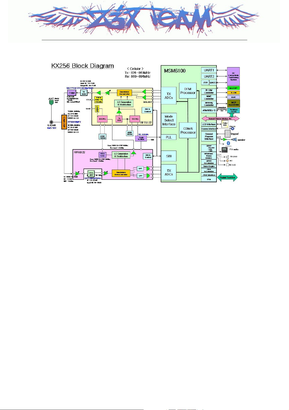
The RF transmit/receive part employs the direct conversion architecture (ZIF,
Zero Intermediate Frequency). The transmit/receive frequency is respectively
824.04~848.97MHz and 869.04~893.97MHz. The block diagram is shown in
[Figure 1-1].RF signals received through the antenna are fed into RFR6122
through the duplexer. And then, they pass the low noise amplifier (LNA),
combined with the signals of local oscillator (VCO) at the frequency mixer in
order to create baseband signal directly. Baseband signals created are
changed into digital signals by the analog / digital converter (ADC, A/D
Converter) and then, auto gain controlled and, sent to the MSM6100 (Mobile
Station Modem) of the digital circuit part. Then, they are demodulated by the
modulator / demodulator. In the case of transmission, MSM6100 modulates,
interpolates, and converts the digital signal into an analog baseband before
sending it to the RFT6122. RFT6122 receives OQPSK-modulated anlaog
baseband signals from the MSM6100’s Tx part. The RFT6122 upconverts the
Tx analog baseband into RF. The RFT6122 connects directly with MSM6100
using an analog baseband interface. In RFT6122, the baseband quadrature
signals are upconverted to the Cellular Tx frequency bands and amplified to
provide signal drive capability to the power amp. After that, the RF signal is
amplified by the Power Amp in order to have enough power for radiation.
Finally, the RF signal is sent out to the cell site via the antenna after going
through the duplexer.
Z3X-BOX.COM
UD/ID256/RD6600
4
[Figure 1-1] Block Diagram of KX256
1.1.2 Description of Receive Part Circuit
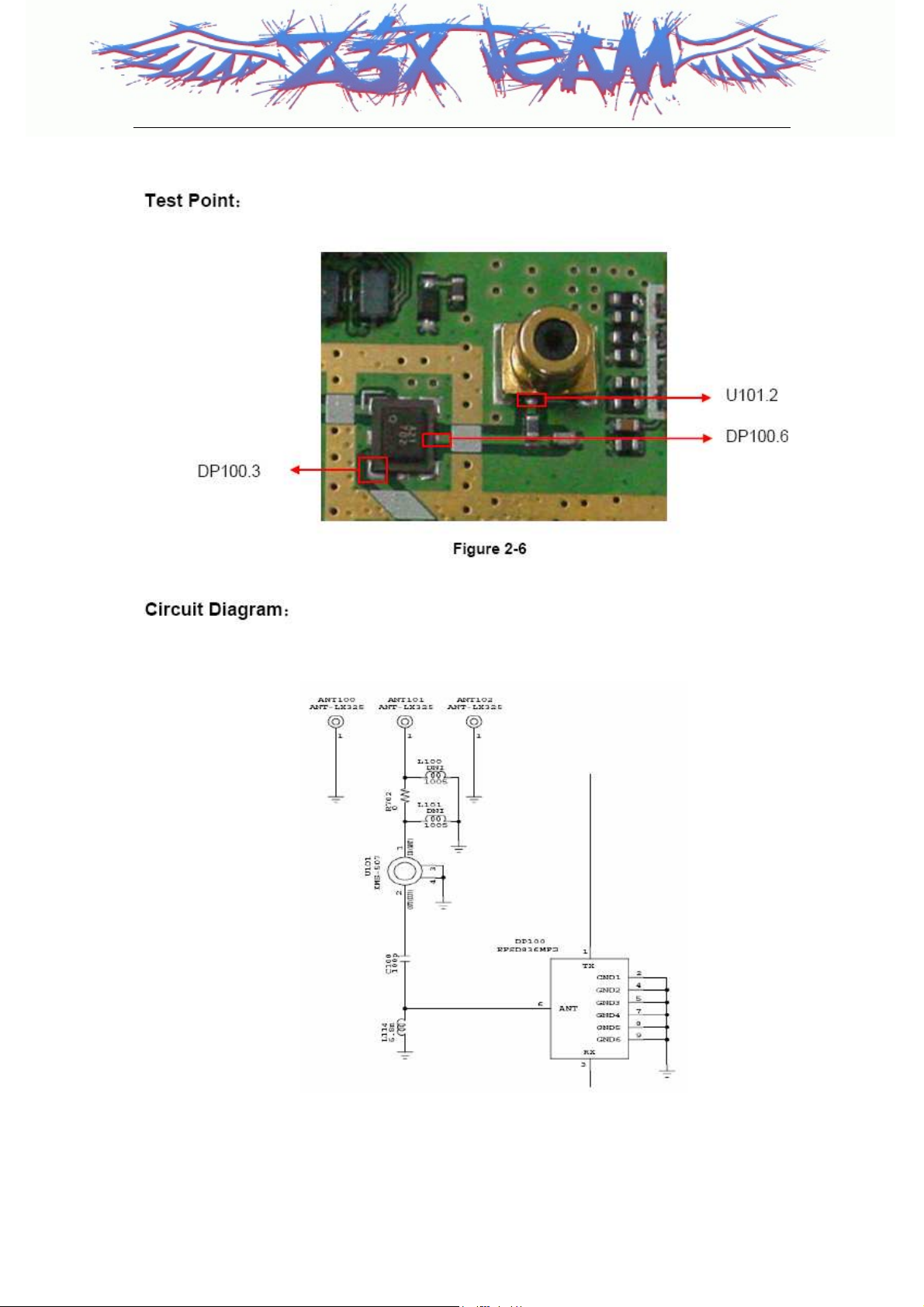
1.1.2.1 Duplexer (DP100)
The duplexer consists of the receive part bandpass filter (BPF) and the
transmit part bandpass filter (BPF) which have the function of separating
transmit/receive signals in the full duplex system using the transmit/receive
common antenna. The transmit part BPF is used to suppress noises and
spurious waves entering the receive band among transmit signals in order to
prevent the drop in receive sensitivity characteristics. The receive part BPF
blocks the signals sent out from entering the receive end in order to improve
sensitivity characteristics.
Insertion loss (IL) in the transmit band is 2.8dB (Max), whereas IL in the
receive band is 2.1dB (Max). The receive band attenuation amount of transmit
filter is 51dB (Min) and the transmit band attenuation amount of receive filter is
45dB or more (Min).
Z3X-BOX.COM
UD/ID256/RD6600
5
1.1.2.2 LNA (U106)
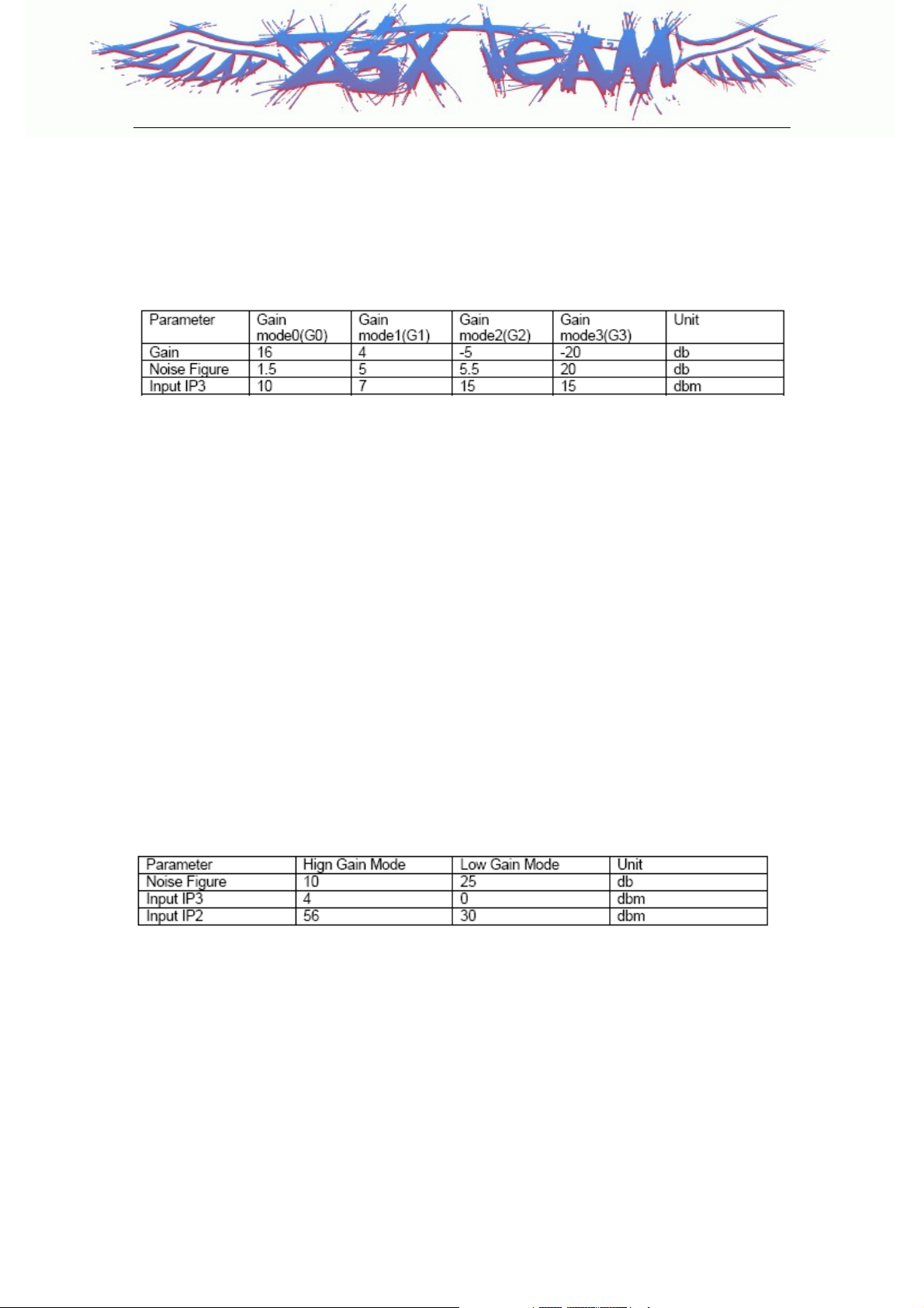
The RFR6122 has cellular LNA. The characteristics of Low Noise Amplifier
(LNA) are low noise figure, high gain, high intercept point and high reverse
isolation. The frequency selectivity characteristic of mobile phone is mostly
determined by LNA.
The specifications of KX256 LNA are described below
1.1.2.3 Rx RF SAW FILTER (F100)
The main function of Rx RF SAW filter is to attenuate mobile phone spurious
frequency, attenuate noise amplified by the LNA and suppress second
harmonic originating in the LNA.
1.1.2.4 Down-Converter Mixers (U106)
The RFR6122 device performs signal direct-down-conversion for Cellular
applications. It contains all the circuitry (with the exception of external filters)
needed to support conversion of received RF signals to baseband signals.
The LO Buffer Amplifier buffers the RF VCO to the RF Transmit Upconverter.
RFR6122 offers the most advanced and integrated CDMA Rx solution
designed to meet cascaded Noise Figure (NF) and Third-order Intercept Point
(IIP3) requirements of IS-98C and J-STD-018 specifications for Sensitivity,
Two-Tone Intermodulation, and Single-tone Desense.
Operation modes and band selection are specially controlled from the Mobile
Station Modem MSM6100. The specification of KX256 Mixers are described
below:
Z3X-BOX.COM
1.
1.1.3 Description of Transmit Part Circuit
1.1.3.1 Description on the Internal Circuit of MSM6100 (U202) and
RFT6122 (U105)
For the transmit data path(Tx), the MSM6100 modulates, interpolates, and
converts the digital signal into an analog baseband before sending it to the
RFT6122. The RFT6122 upconverts the Tx analog baseband into RF. The
MSM6100 communicates with the external RF and analog baseband to control
UD/ID256/RD6600
6
signal gain in the RF Rx and Tx signal paths, educe base band offset errors,
and tune the system frequency reference.
The RFT6122 baseband-to-RF Transmit Processor performs all Tx
signalprocessingfunctions required between digital baseband and the Power
Amplifier Module (PAM). The baseband quadrature signals are upconverted to
the Cellular frequency bands and amplified to provide signal drive capability to
the PAM. The RFT6122 includes an mixer for up-converting analog baseband
to RF, a programmable PLL for generating Tx and Rx LO frequency, cellular
driver amplifier and Tx power control through an 85 dB VGA. As added benefit,
the single sideband upconversion eliminates the need for a band-pass filter
normally required between the upconverter and driver amplifier.
I, I/, Q and Q/ signals proceed from the MSM6100 to RFT6122 are analog
signal. In CDMA mode,These signals are modulated by Offset Quadrature
Phase Shift King (OQPSK). I and Q are 90 deg. out of phase, and I and I/ are
180 deg. The mixer in RFT6122 converts baseband signals into RF signals.
After passing through the upconverters, RF signal is inputted into the Power
Amplifier Module.
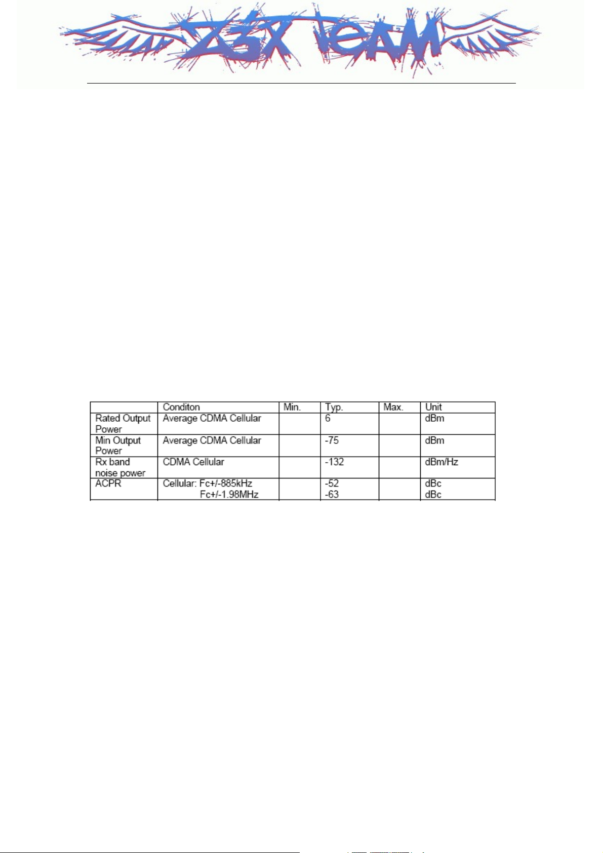
The RFT6122 Cellular CDMA RF specifications are described below:
1.1.3.2 Power Amplifier (U103)
The power amplifier that can be used in the CDMA mode has linear
amplification capability. For higher efficiency, it is made up of one module
(Monolithic Microwave Integrated Circuit) for which RF input terminal and
internal interface circuit are integrated onto one IC after going through the
GaAs HBT (heterojunction bipolar transistor) process.
The module of power amplifier is made up of an output end interface circuit
including this module.The maximum power that can be inputted through the
input terminal is +7dBm and conversion gain is about 28.5dB. RF transmit
signals that have been amplified through the power amplifier are sent to the
duplexer.
Z3X-BOX.COM

UD/ID256/RD6600
7
1.1.4 Description of Frequency Synthesizer Circuit
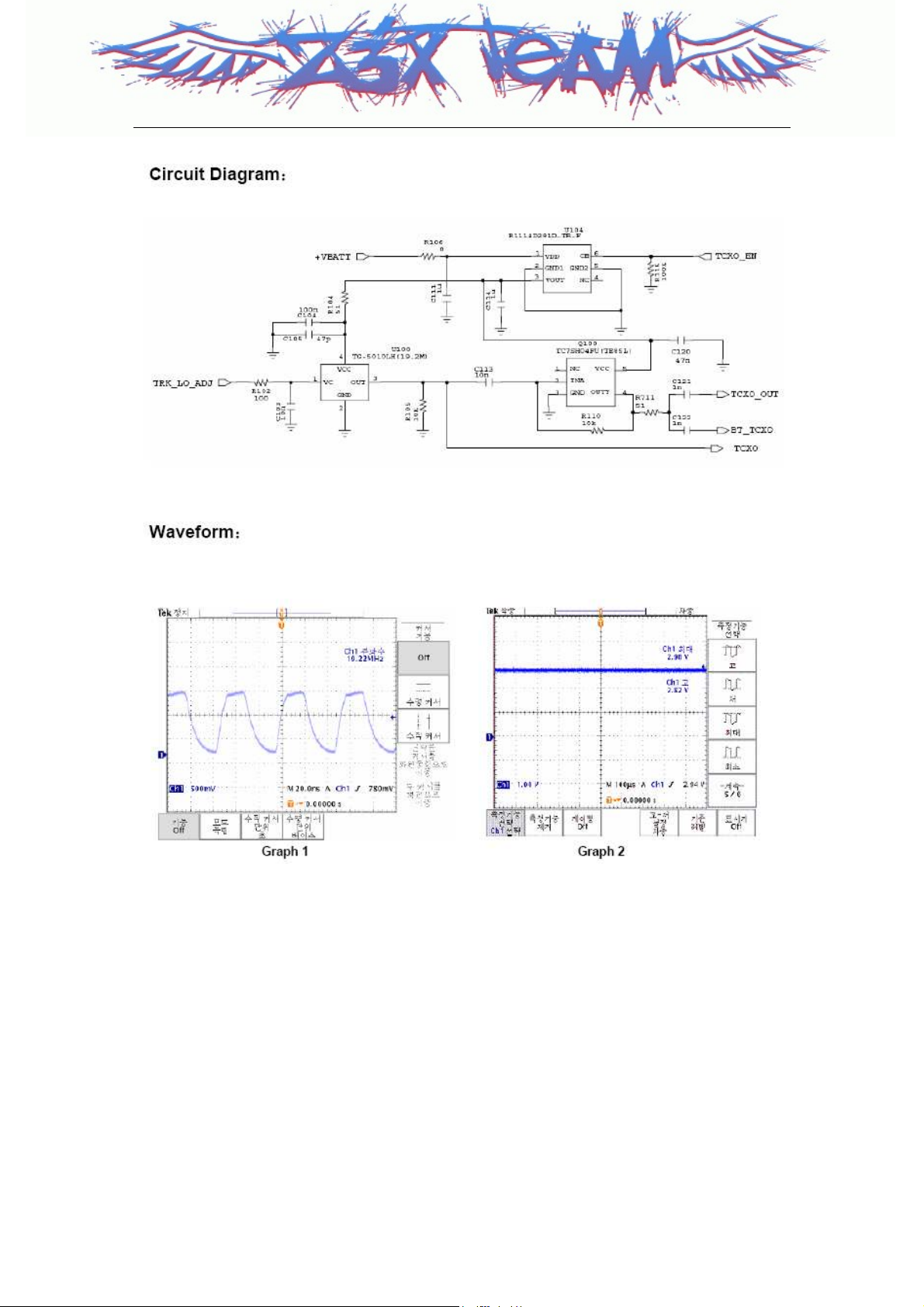
1.1.4.1 Voltage Controlled Temperature Compensation Crystal
Oscillator (U100)
The temperature range that can be compensated by VC-TCXO which is the
reference frequency generator of a mobile station is -30~+80 °C.
VC-TCXO receives frequency tuning signals called TRK_LO_ADJ from
MSM6100 as 0.5V~2.5V DC via R and C filters in order to generate the
reference frequency of 19.20MHz and input it into the frequency synthesizer
of UHF band. Frequency stability depending on temperature is ±2.0 ppm.
1.1.4.2 Voltage Controlled Oscillator (U106)
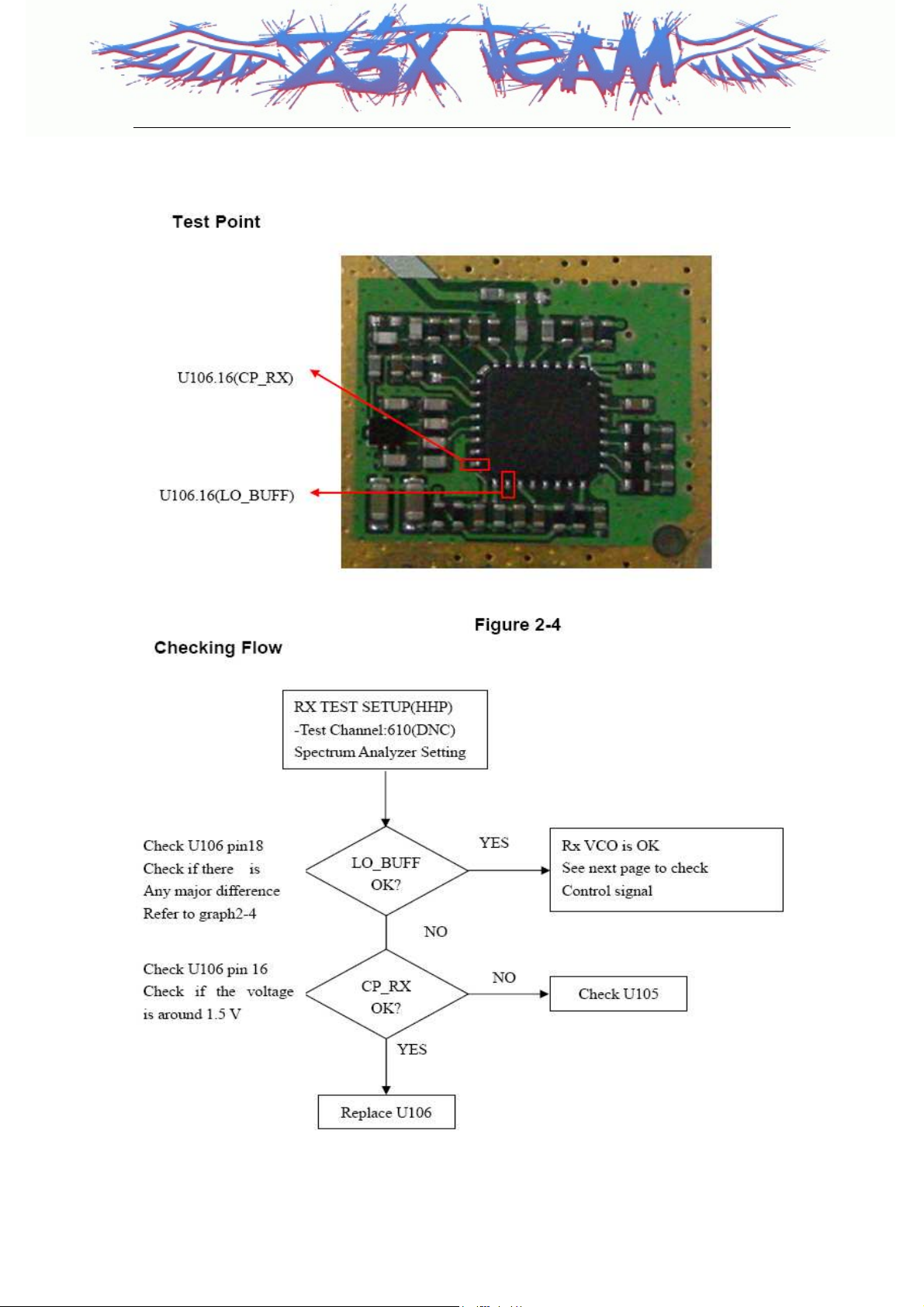
The internal VCO signal of RFR6122 is processed by the LO generation and
distribution circuits in RFR6122 to create Cellular quadrature downconverter’
s LO signals. The LO signals applied at the mixer ports are at the frequency
different than the VCO frequency. This assures that the VCO frequency is
different than the RF frequency, an important consideration for Zero-IF
processing. The VCO frequency used are 1738.08~1787.94MHz for cellular
and It is produced in single voltage controlled oscillator of U106.
1.2 Digital/Voice Processing Part
1.2.1 Overview
The digital/voice processing part processes the user's commands and
processes all the digital and voice signal processing in order to operate in the
phone. The digital/voice processing part is made up of a keypad/LCD,
receptacle part, voice processing part, mobile station modem part, memory
part, and power supply part.
1.2.2 Configuration
1.2.2.1 Keypad/LCD and Receptacle Part
This is used to transmit keypad signals to MSM6100. It is made up of a keypad
backlight part that illuminates the keypad, LCD part that displays the operation
status on to the screen, and a receptacle that receives and sends out voice
and data with external sources.
Z3X-BOX.COM

UD/ID256/RD6600
8
1.2.2.2 Voice Processing Part
The voice processing part is made up of an audio codec in MSM6100 used to
convert MIC signals into digital voice signals and digital voice signals into
analog voice signals, amplifying parts for amplifying the voice signals and MIC
signals are on Codec in MSM6100.
1.2.2.3 MSM6100 (Mobile Station Modem) Part
MSM6100 is the core elements of a CDMA mobile station and carries out the
functions of CPU, encoder, interleaver, deinterleaver, Viterbi decoder,
Mod/Demod, codec, and vocoder.
1.2.2.4 Memory Part
The memory part is made up of a flash memory and a SDRAM
1.2.2.5 Power Supply Part
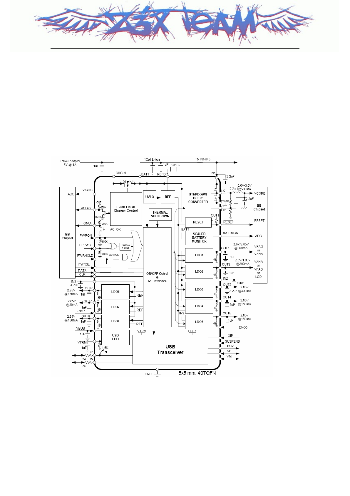
The PMIC(MAX1829) is made up of 8 Regulators and one DCDC direct connet
to Batt.
Out1 give the power each Circuits(RFT6122/RFR6122).
Out1 and DCDC gives the power to the MSM and memory parts.
PAM, Motor, LCD back light LED, Keypad LED and Audio amplifier, are directly
conneted to Battery.
1.2.3 Circuit Description
1.2.3.1 Keypad/LCD and Receptacle Part
Once the keypad is pressed, the key signals are sent out to MSM6100 for
processing. In addition, when the key is pressed, the keypad lights up through
the use of 10 LEDs. The status and operation of a mobile station are displayed
on the screen for the user with the characters and icons on the LCD.
Receptacle(CON601) exchanges audio signals and data with external sources
and then, receives power from the battery or external batteries.
Z3X-BOX.COM
1.2.3.2 MSM Part
MSM6100 is the core element of a CDMA mobile station. Subsystems within
the MSM6100 include a CDMA processor, an EVRC(Enhanced Variable Rate
Codec) vocoder, an ARM926EJ-S microprocessor ,and assorted peripheral
interfaces that are used to support other functions. MSM6100, when operated
in the CDMA mode, utilizes TCXO (19.2MHz) as the reference clock primarily for
CDMA and vocoder processing.MSM6100 also uses TCXO/4 (4.92MHz).
The CPU controls total operations of the subscriber unit. Digital voice data,

UD/ID256/RD6600
9
that have been inputted, are encoded using the EVRC algorithm. Then, they
are convolutionally encoded so that error detection and correction are
possible. Coded symbols are interleaved in order to avoid a burst error.
Each data channel is scrambled by the long code PN sequence of the user in
order to ensure the confidentiality of calls. Moreover, binary quadrature codes
are used based on Walsh functions in order to discern each channel. Data
created thus are 4-phase modulated by one pair of Pilot PN code and they are
used to create I and Q data. When received, I and Q data are demodulated
into symbols by the demodulator and then, de-interleaved in reverse to the
case of transmission. Then, the errors of data received from Viterbi decoder
are detected and corrected. They are voice decoded at the vocoder in order to
output digital voice data.
The MSM6100 also supports Enhanced Variable Rate Coder (EVRC) operation
in addition to the standard 13k.
1.2.3.2.1 Audio Processing Part
MIC signals are inputted into the audio codec, and amplified with
programmable gain, and converted into digital signals(PCM). Then, they are
inputted into MSM6100. In addition, digital audio signals(PCM) outputted from
MSM6100 are converted into analog signals after going through the audio
codec. These signals are amplified with programmable gain on codec’s
internal AMP and external Audio AMP and then transferred to the ear piece.
The signals is generated in MSM6100 using SW MIDI.
1.2.3.3 Memory Part
The memory part consists of a 512Mbits Flash Memory and a 256Mbits SDRAM.
In the Flash Memory, there are programs used for the operation of a mobile
station. The programs can be changed through down loading after the
assembling of mobile stations. The Flash memory is also emulated as an
EEPROM to store Calibration Data, etc. On the SDRAM, data generated during
the operation of a mobile station are stored temporarily.
Z3X-BOX.COM
1.2.3.4 Power Supply Part
Turn ON
When the battery voltage (4.2V ~ 3.3V) is fed and the PWR key of keypad is
pressed, PMIC is activated by the PWR_ON_SW signal, and then the control
signal ON_SW_SEN/ signal is generated. And then, the regurator 1.85V_MSMC
& 2.6V_MSMP, 2.6V_MSMA, are operated.
Operating
During the phone is on operating state,LDO(in PMIC) for MSM is always
enable and gives the power MSM6100 and memory part
UD/ID256/RD6600
10
LDO(in PMIC) for +2.6V_TX part is enabled on IDLE/ state, and gives the
power TX part devices.
LDO(in PMIC) for +2.6V_RX part is enabled on SLEEP/ state, and gives the
power RX part devices.
Turn OFF
When the PWR key is pressed during a few seconds, PMIC is turned on by
PWR_ON_SW and then, 'Low' is outputted on ON_SW_SEN/. MSM6100
receives this signal and then, recognizes that the POWER key has been
pressed. During this time, MSM6100 outputs PS_HOLD as low and turn off all
devices
Z3X-BOX.COM
Figure 1-2] Block Diagram Of Power Management IC
[
1.2.3.5 Logic Part
The Logic part consists of internal CPU of MSM6100, PSEUDO RAM & FLASH
MEMORY.The MSM6100 receives TCXO/4 clock(19.20Mz) and CHIPX8 clock

UD/ID256/RD6600
11
signals, and then controls the phone during the CDMA and the FM mode. The
major components are as follows:
CPU : ARM926EJ-S microprocessor core
MEMORY : 512Mbit NAND Flash + 256Mbit SDRAM.
CPU (U202)
ARM926EJ-S 32-bit microprocessor is used and CPU controls all the circuitry.
Some of the features of the ARM microprocessor include a 3 stage pipelined
RISC architecture, both 32-bit ARM and 16bit THUMB instruction setsm, a
32-bit address bus, and a 32-bit internal data bus.
FLASH Memory (U300)
Flash Memory is used to store the program of the mobile station. Using the
down-loading program, the program can be changed even after the mobile
station is fully assembled.
Pseudo RAM (U300)
SDRAM is used to store the internal flag information, call processing data, and
timer data.
KEYPAD
For key recognition, key matrix is setup using GPIO46,47,49~53,62,63of
output orts of MSM6100. Backlight circuitry are included in the keypad for
easyoperation in the dark.
LCD MODULE
LCD module contains a controller which will display the information onto the
LCD by 16-bit data from the MSM.
It has 262K Color CSTN full graphic 220(W) X 176(H) dots.
Z3X-BOX.COM
UD/ID256/RD6600
12
2. Trouble Shooting
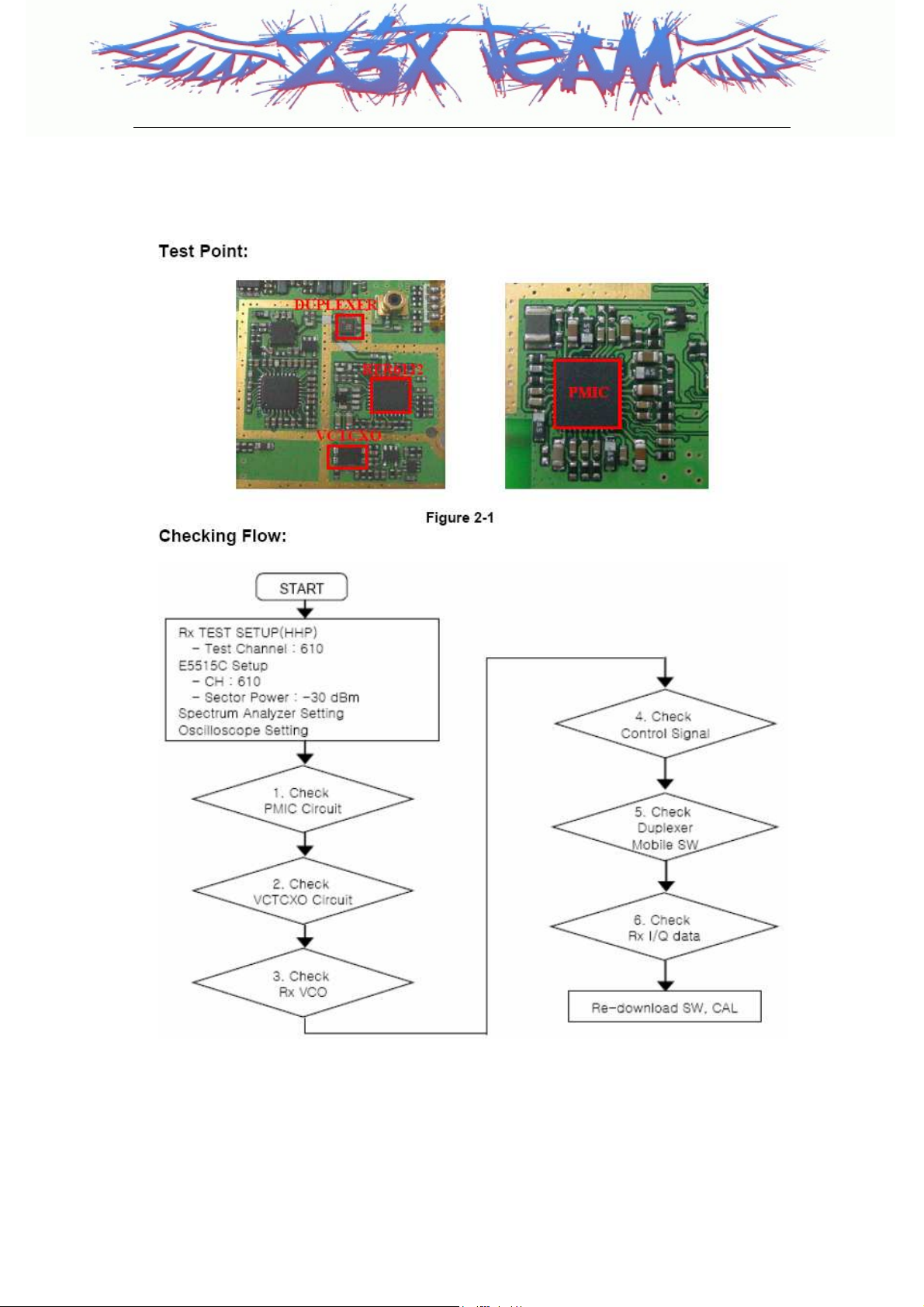
2.1 Rx Part Trouble
Z3X-BOX.COM
UD/ID256/RD6600
13
2.1.1 Checking Regulator Circuit
Z3X-BOX.COM

UD/ID256/RD6600
14
2.1.2 Checking VCTCXO Circuit
Z3X-BOX.COM
UD/ID256/RD6600
15
Z3X-BOX.COM
UD/ID256/RD6600
16
2.1.3 Checking Rx VCO Signal
Z3X-BOX.COM
UD/ID256/RD6600
17
2.1.4 Checking Control Signal
Z3X-BOX.COM
UD/ID256/RD6600
18
Z3X-BOX.COM
UD/ID256/RD6600
19
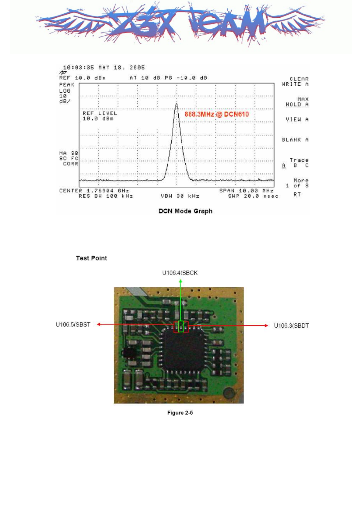
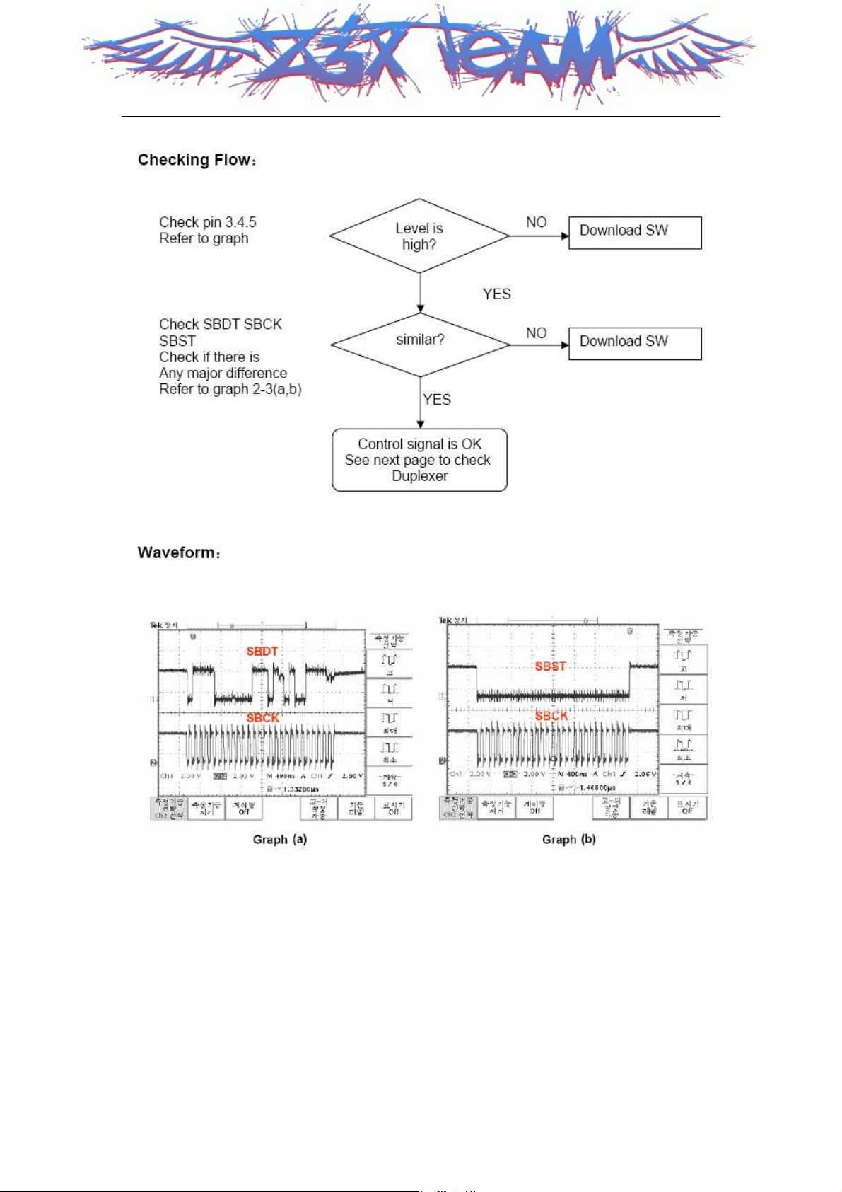
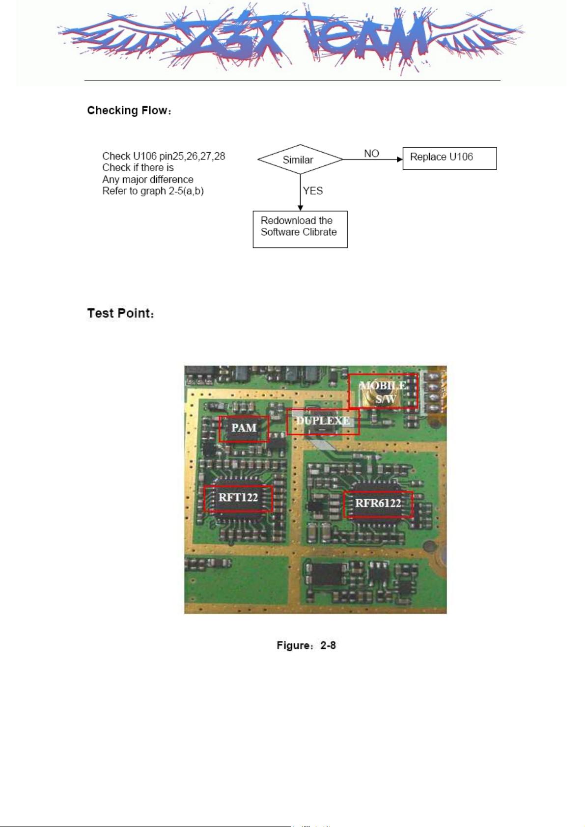
2.1.5 Checking Mobile SW & Duplexer(DCN,PCS)
Z3X-BOX.COM
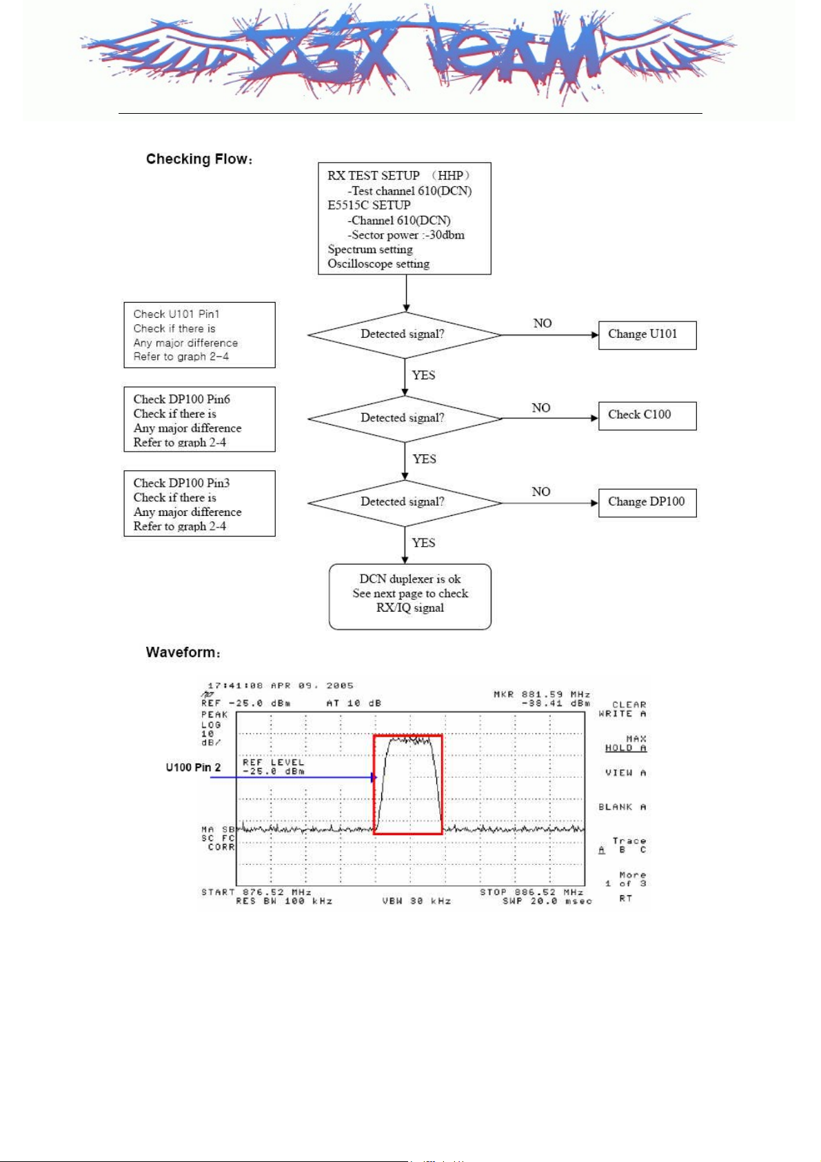
UD/ID256/RD6600
20
Z3X-BOX.COM
UD/ID256/RD6600
21
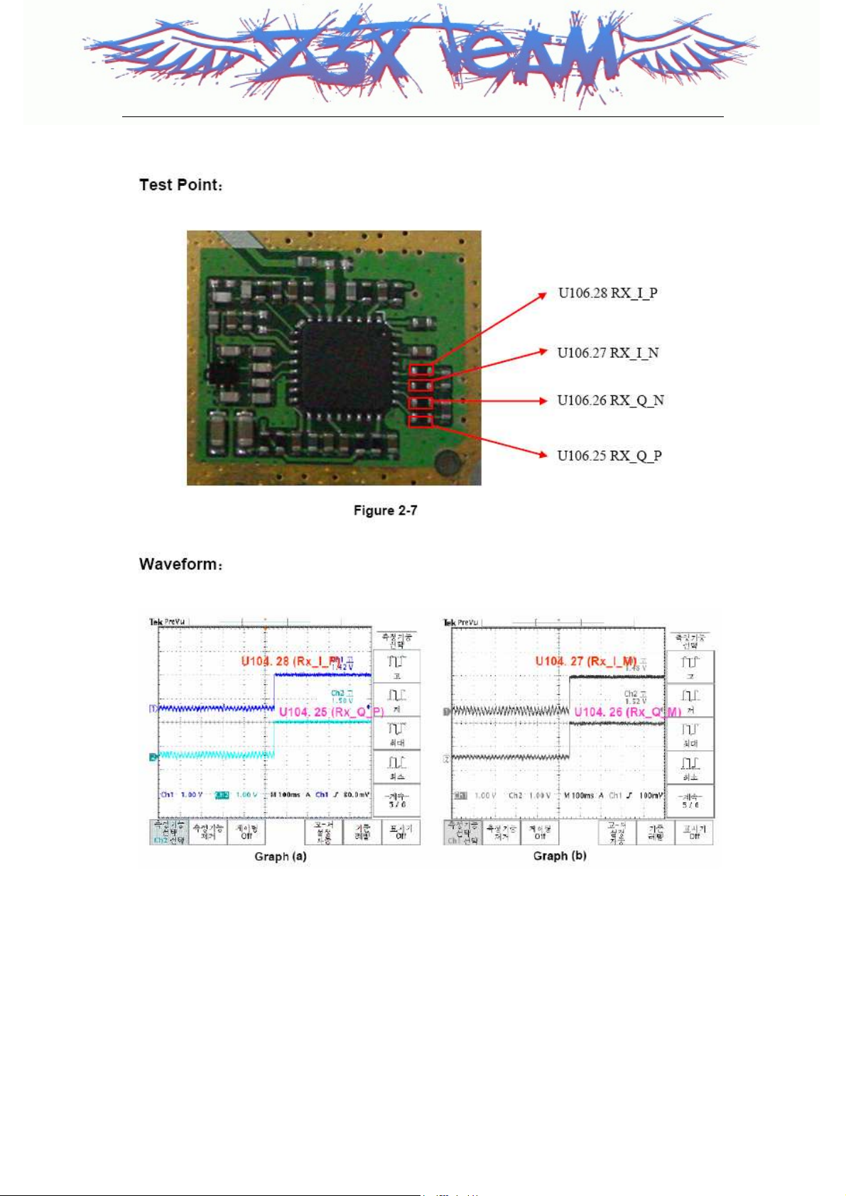
2.1.6 Checking Rx I/Q data
Z3X-BOX.COM
UD/ID256/RD6600
22
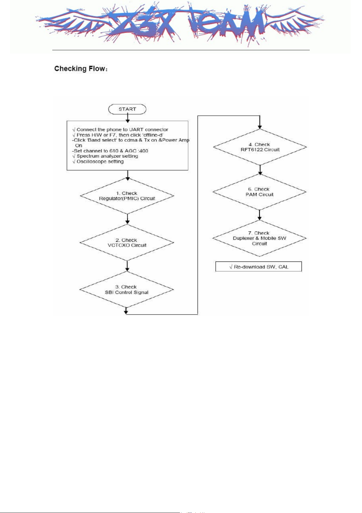
2.2 Tx Part Trouble
Z3X-BOX.COM
UD/ID256/RD6600
23
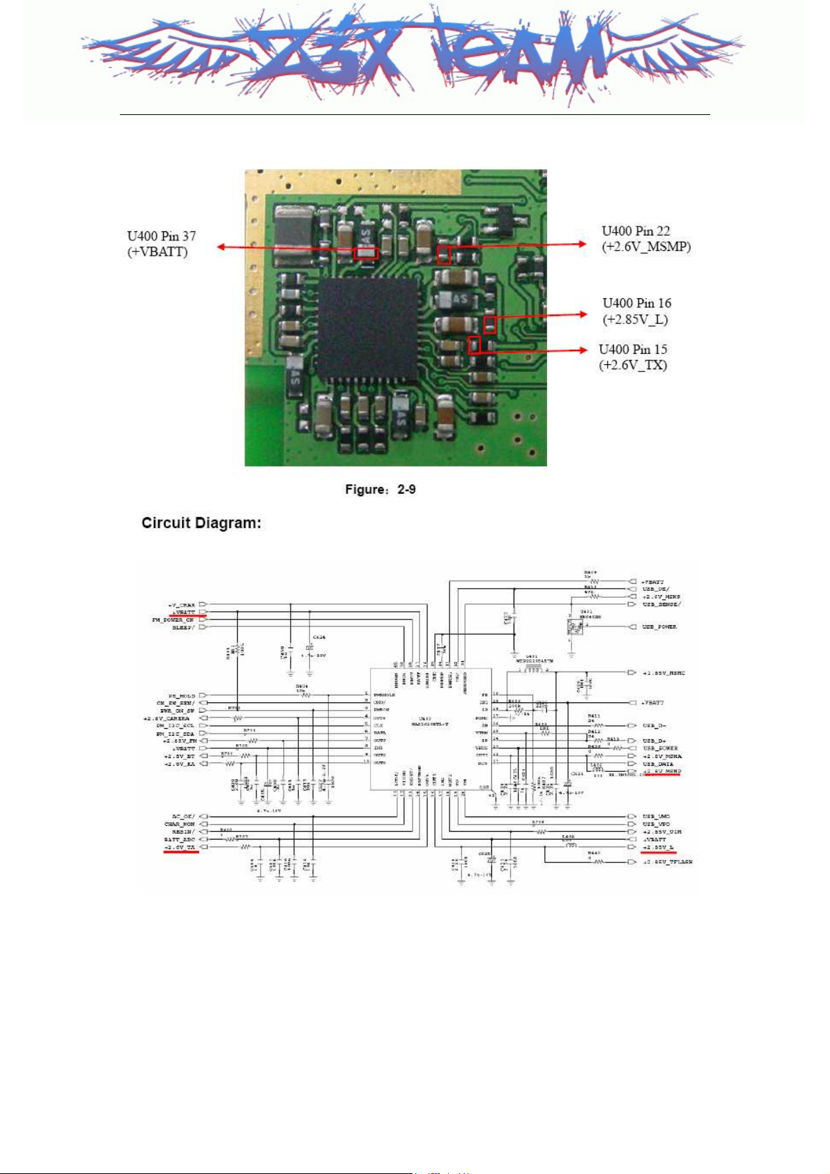
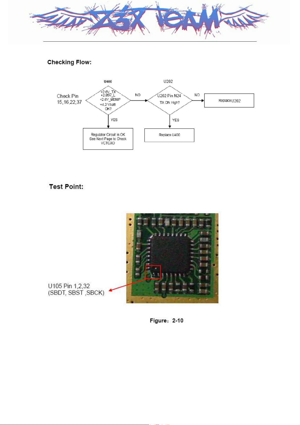
2.2.1 Check Regulator(PMIC) Circuit
Test Point:
Z3X-BOX.COM
UD/ID256/RD6600
24
Z3X-BOX.COM
UD/ID256/RD6600
25
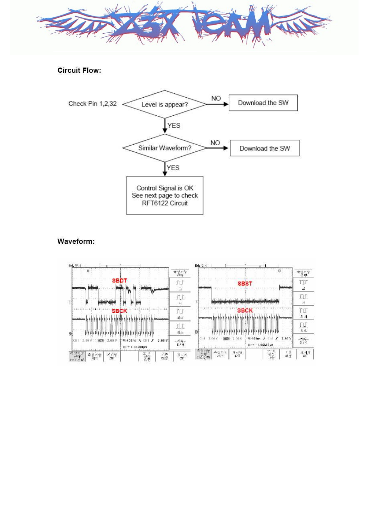
2.2.2 Check SBI Control Signal
Z3X-BOX.COM
UD/ID256/RD6600
26
Z3X-BOX.COM
UD/ID256/RD6600
27
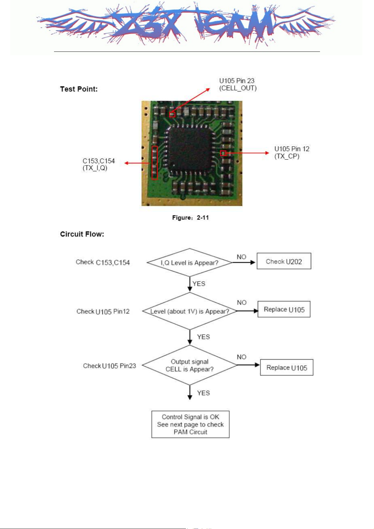
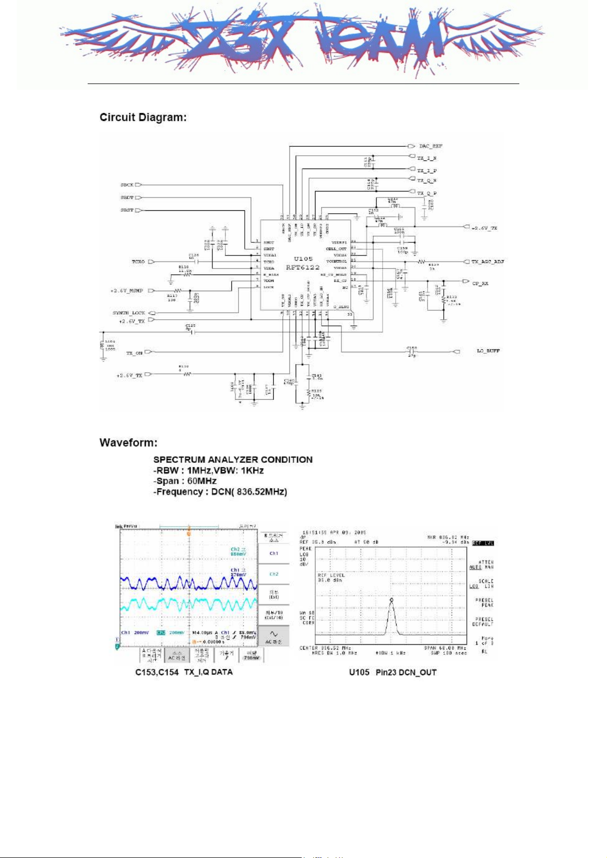
2.2.3 Check RFT6122 Circuit
Z3X-BOX.COM
UD/ID256/RD6600
28
Z3X-BOX.COM
UD/ID256/RD6600
29
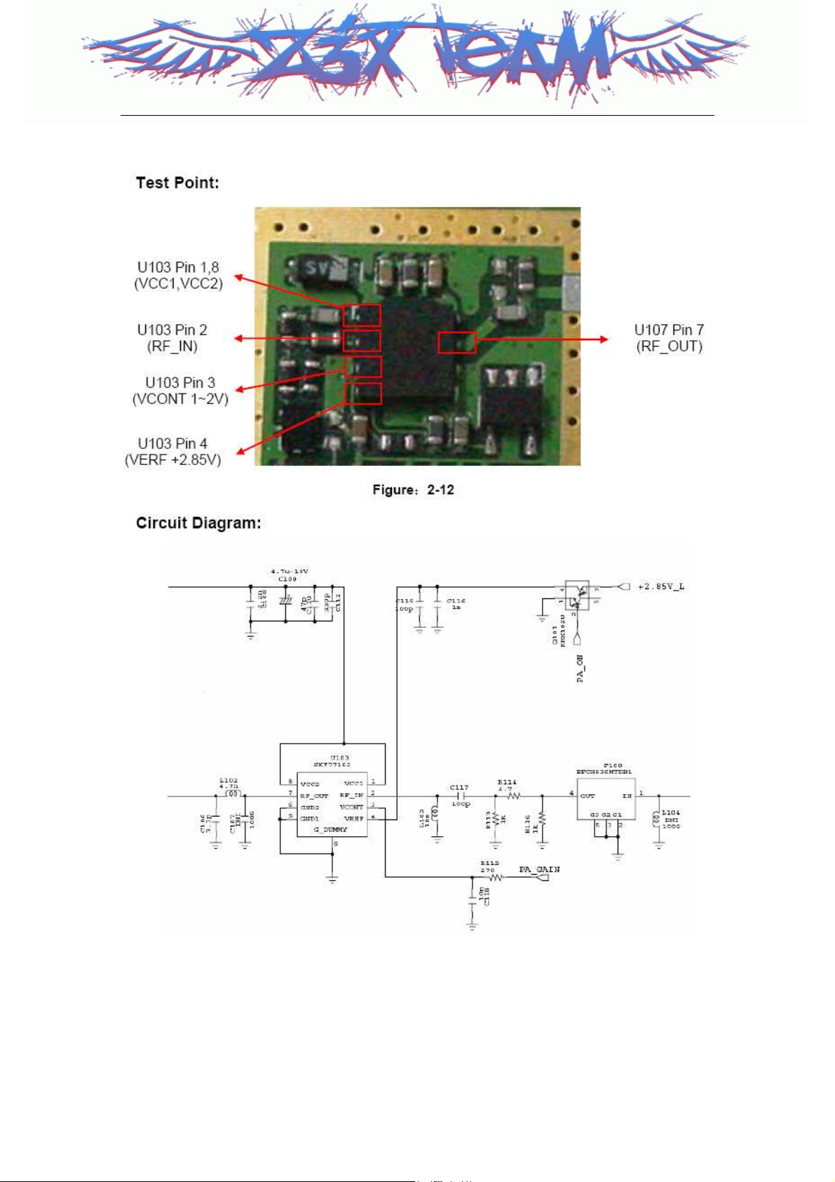
2.2.4 Check PAM Circuit
Z3X-BOX.COM
 Loading...